Task to be Perform for this week
1) Group Assignment : Use the test equipment in your lab to observe the operation of a microcontroller circuit board.
2) Individual project: We need redraw an echo hello-world board, add (at least) a button and LED (with current-limiting resistor), check the design rules, make it, and test it extra credit: simulate its operation
Introduction to Electronics Design
Electronic gadgets have become an integral part of our lives. They have made our lives more comfortable and convenient. From aviation to medical and healthcare industries, electronic gadgets have a wide range of applications in the modern world. In fact, the electronics revolution and the computer revolution go hand in hand.
Most gadgets have tiny electronic circuits that can control machines and process information. Simply put, electronic circuits are the lifelines of various electrical appliances. This guide explains in detail about common electronic components used in electronic circuits and how they work.
Most electronic appliances require complex electronic circuits. That’s why designers have to arrange tiny electronic components on a circuit board. It comprises a plastic board with connecting copper tracks on one side and lots of holes to affix the components. When the layout of a circuit board is printed chemically onto a plastic board, it is called a printed circuit board or PCB.
Source:Electronics Design
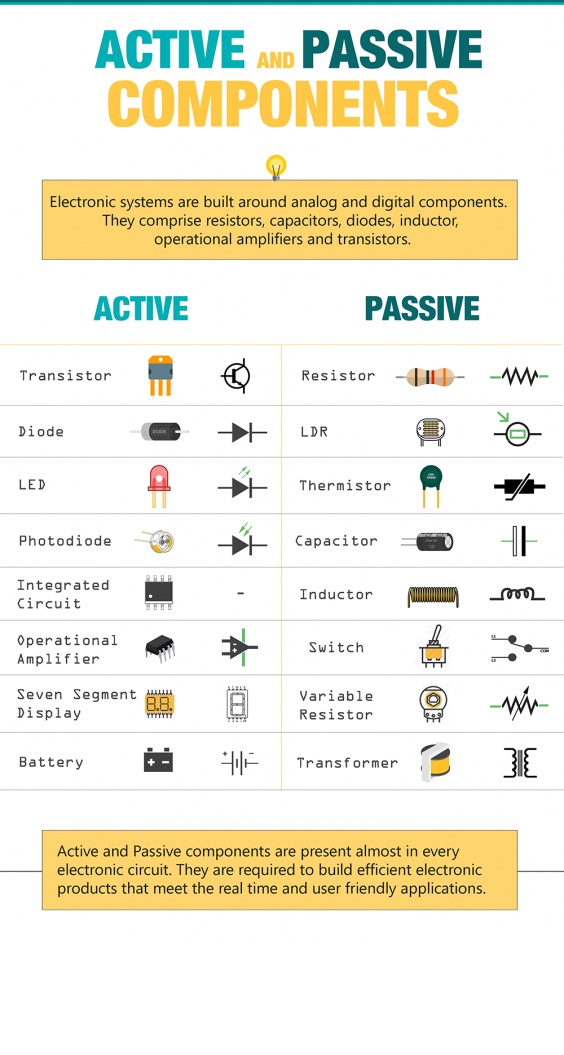
All Electronic components can be broadly classified into two classes, namely Active Components and Passive components.
What are Active Components?
Active components are devices that can amplify an electric signal and produce power. Any characteristic active component will comprise an oscillator, transistor or an integrated circuit. An active component functions as an alternating current circuit in devices. This helps the device to augment power and voltage. This component can execute its operations because it is powered by a source of electricity. All active components necessitate some source of energy which commonly is extracted from a DC circuit.
What are Passive components?
Passive components cannot control electric current utilizing a second electrical signal. Some important passive components are capacitors, resistors, inductors, and transformers. Passive components do not require energy to operate barring the AC circuit. Unlike the Active component, they are unable to augment the signal power and also cannot amplify it. There are majorly two types of passive components namely.
Group Assignment:-In this week of group Assignment We have tested all the electronics Equipment available in our lab to observed the operation of Microcontroller Circuit Board. Individual Assignment: In case of individual assignment the task for this week is to redraw an echo hello-world board, provided by Fab Academy and add (at least) a button and LED (with current-limiting resistor), check the design rules, make it, and test it. So to redraw the echo hello-world, I used Eagle software.
Learning outcomes
Select and use software for circuit board design
Demonstrate workflows used in circuit board design
About Eagle Software for PCB designing
EAGLE is electronic design automation (EDA) software that lets printed circuit board (PCB) designers seamlessly connect schematic diagrams, component placement, PCB routing and comprehensive library content.
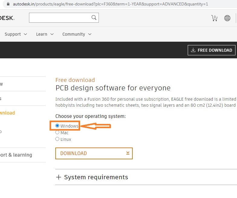
Firstly I have downloaded from eagle the software and installed it in my laptop.
Find the link for download this software HereEagle software link
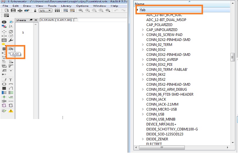
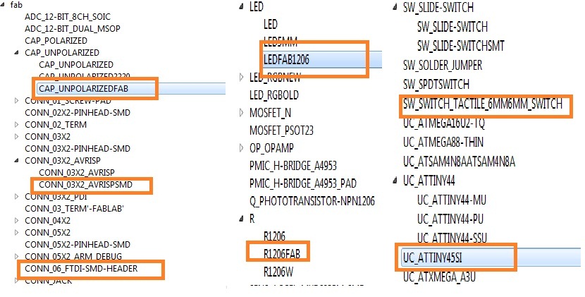
Then I have upadted some libraries from link given by fabacedemy and extract that in my folder from here i.e. fab.lbr and atmel.lbr
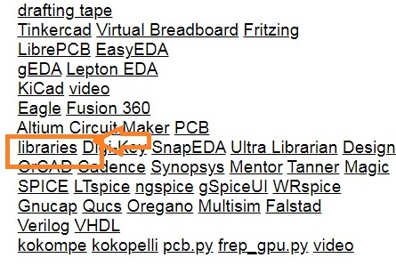
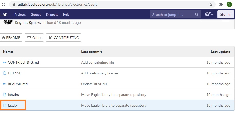
The link of fab library is found to be here fab.lbr
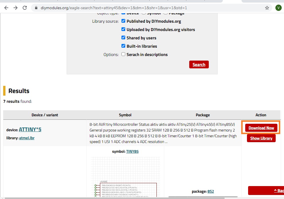
The libraries for attiny45 i have downloaded from thisLINK
Once downloaded this i need to use above libraries in Eagale software
Then I have reffered list of microcontroller given on fab acedemy website and choose to draw ATtiny45 which is suitable for me.
I have download this board file from fabacademy websites LINK here
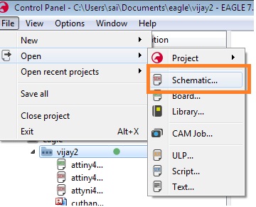
After that i have started to draw the above design by using Eagle software
Step to draw a design in eagle software:
1) I have open the eagle software and installed required Fab libraries.
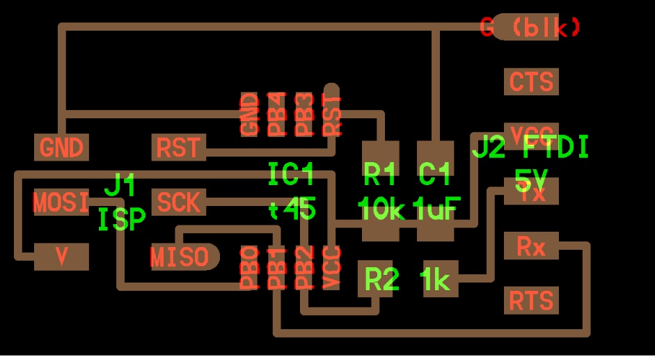
2) I have to go in menu bar in the schematic and click on add->> in add task found the fab where i got the required component to design the pcb and added Button and one LED with resistor
3) Before connection i have reffered the pin configurations of attiny 45 i.e I/O port
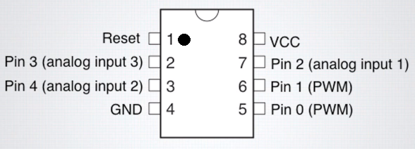
Features of Attiny45 Microcontroller
ATtiny45 is one of the most popular microcontrollers due to its small size and multiple features. This microcontroller available in multiple embedded systems and even you can find its applications at the industrial level.
ATtiny45 microcontroller allows the designer to optimize power vs performance through programming. It is designed by using AVR and RSIC technology which makes it less power consumption controller and usage of its internal oscillator make it save more power. In short, most of the developing board and student project uses ATtiny85 to minimize the size of the project, also the size of the microcontroller can be reduced more by using its different packages.
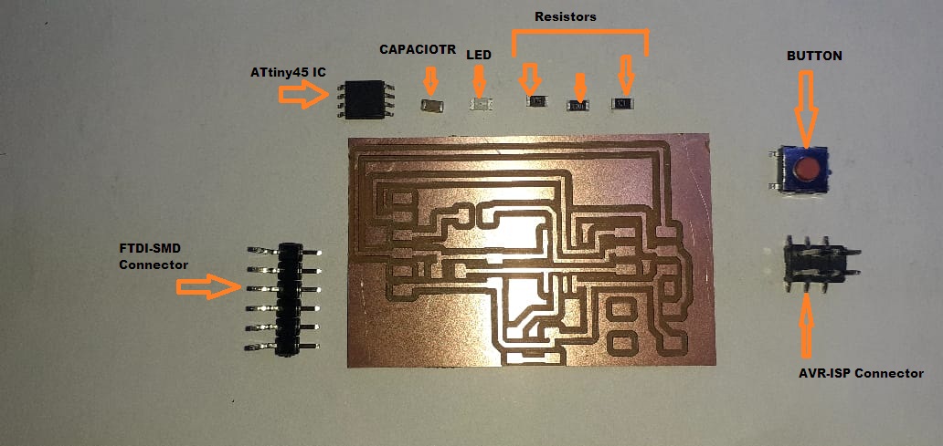
List of required component used in my Echo Hello world Board is as follow
1. Capacitor 1 Nos.
2. Resistor 3 Nos.
3. AVRISPsmd Connector 1 Nos.
4. FTDI-SMD Header connector 1 Nos.
5. Attiny45 Microcontroller IC 1 Nos.
6. LED 1 Nos.
7. Button 1 Nos.
About Used of Eagle Software
Left Toolbar in Eagle PCB:
This toolbar has a multitude of options that require explanation. Overall, this toolbar has the important options when creating your schematic. It allows you to add a part, add a electrical net connection, and more. Before continuing, make sure you understand the definitions and acronyms in PCB design.
Initially we didn't used eagle software to Design the PCB Board.
So one of the member of our fablab course Mr. Mohit Ahuja took one introductory session on " Designing The PCB Through Eagle"
After that i have started to design my PCB Board
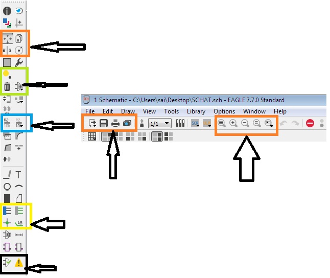
The highlighted red box on the left shows the open, save, and print options for your schematic. The right box shows the zoom to fit, in/out, and selected zoom.
1) Move, Copy, and Rotate (red box)
Move a object around the schematic window
Copy an object, e.g. resistor, in order to paste it
Rotate an object by 90 degrees
2) Paste, delete, and add a part (green box)
If you copied an object, then you can paste it using this command
Cick the delete box then click the object you want deleted
Adding a part option allows you to add components, e.g. ICs, resistors.
3 )Name and value options (blue box)
Change the name of the component for clarity
Change the value of the component
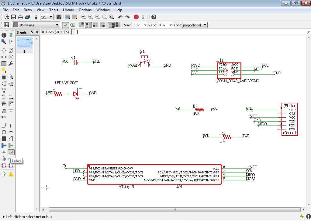
4) Draw a wire connection, place a junction and label (yellow)
Draw a wire between two components to make an electrical connection
Place a junction between two connections
Place the name of the component as a label
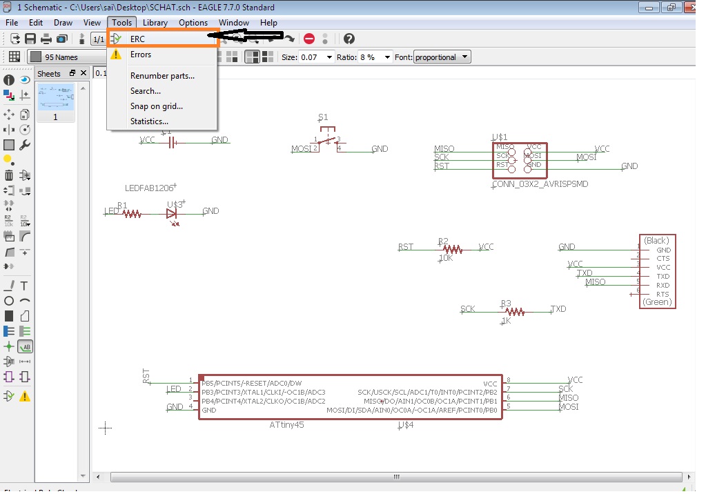
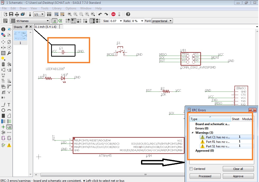
5) Electrical Rule Check (ERC) and see errors/warnings (black)
Run the ERC to see if your schematic was created properly
Show errors/warnings from the ERC tool
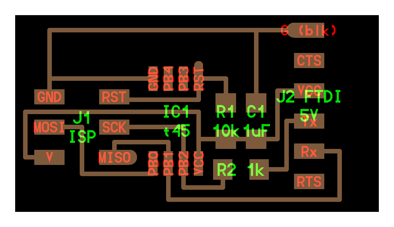
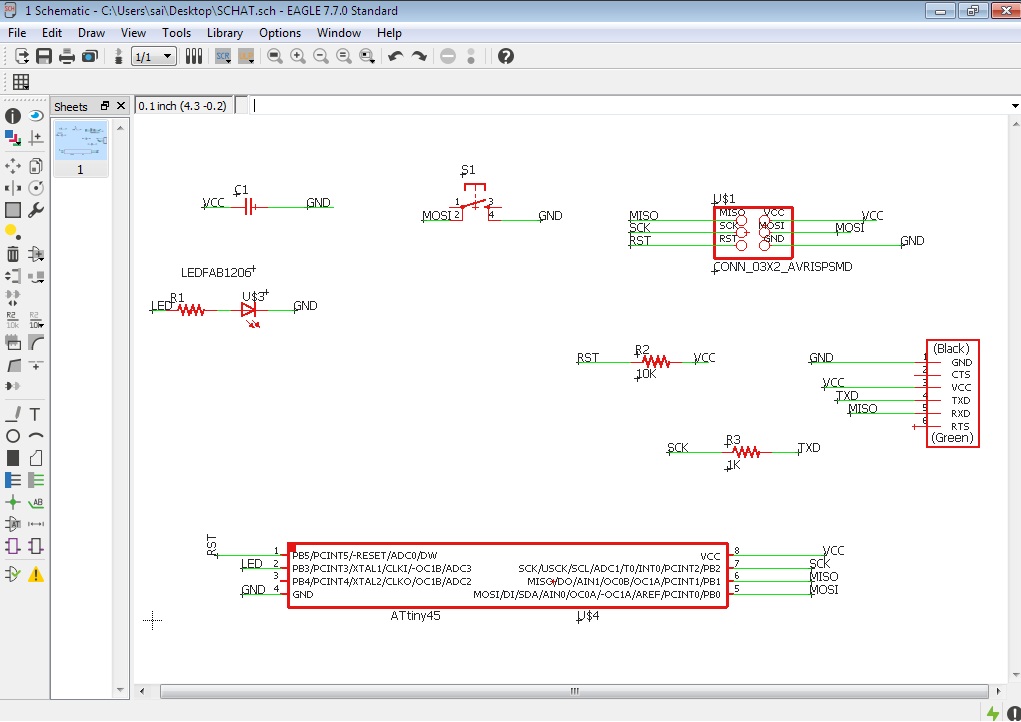
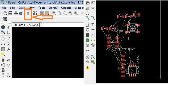
After that i have connect all the component as per circuit diagram using the left toolbar in eagle, and i have used lebel menu for connection,using label menu we can give the tag name of respective pin's
These are the component which i have used for designing the Pcb Board
Then i had checked the ERC i.e. Electrical Rules Check: If any connections is missing it gives the error or does not assign the value to any component it gives the warning
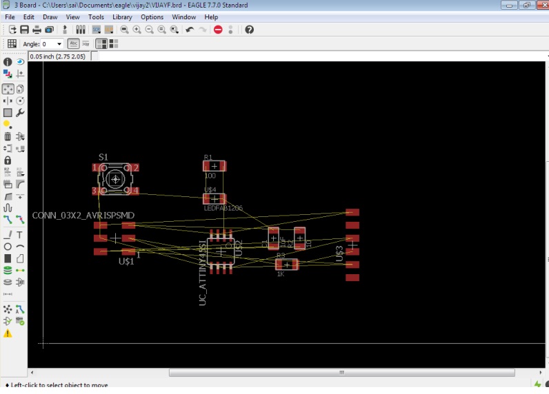
Once the connection is completed i need to switch generate/switch to board this kind of window may open. before arranging the wire, the board is created like this.
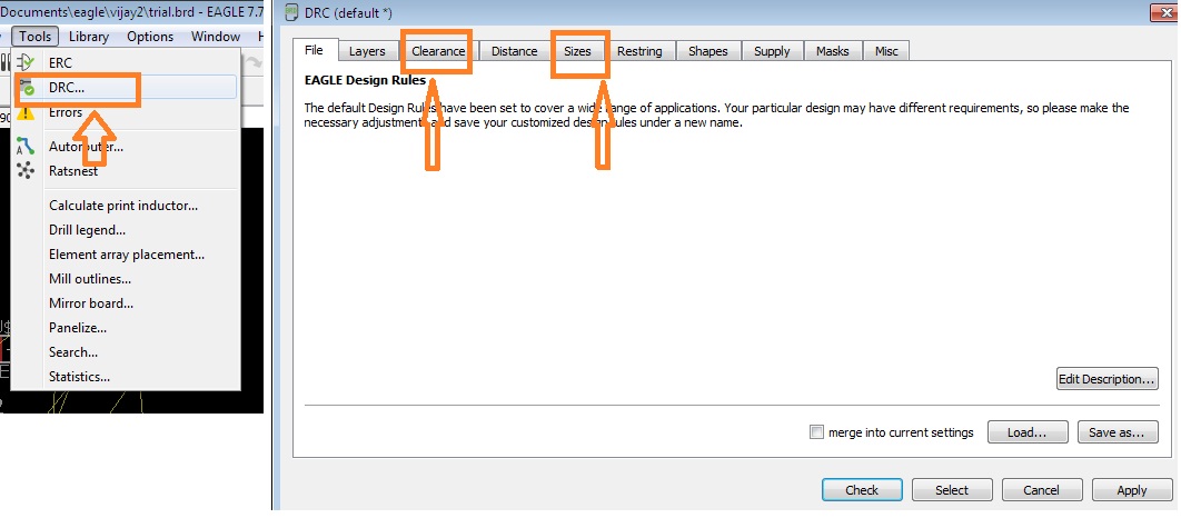
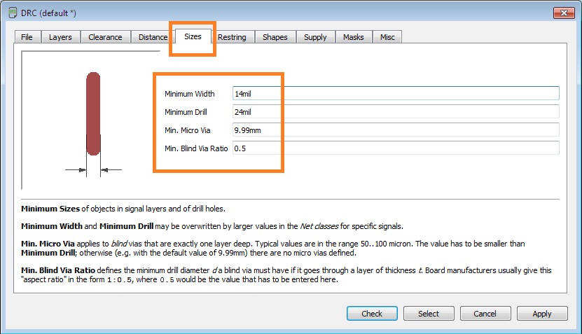
Checked DCR Rules
Now before arranging the component on the board i had to cheked the DCR Rules
PCB board design go through the DRC. DRC means Design rule check is the option provided in the eagle to ckeck the trace width in our board design.
This will help us to design the board by considering all manufacturing limitations
When click on DCR tab the default windows open.
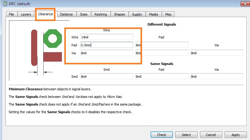
Here i had changed the clearance and sizes and kept rest of the rules is as it is
Arranging the component on PCB Board
After cheking the DCR rules,need to go for arranging the component on the layout should be minimum wires cross each other.
There are bassically two options availble for Routing the PCB Board
We can route the PCB by Auto router or by Route airwire (Hand Routing).
I had tried both the options, first i tried autorouting
when auto routing arrange all the components on the layout.
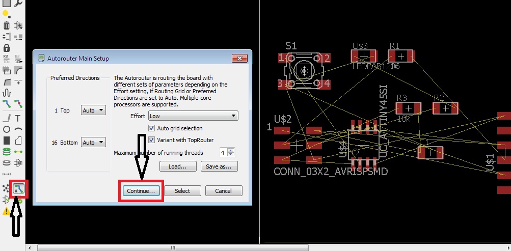
By clicking the Auto router options .in Auto router main setup click on continue.in Routing Variants dialogs click on start, optimize completed. Note that the vias becomes zero and select top router (best auto routed path for given ckt)
But initially vias have not zero
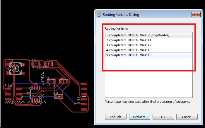
After rearranging the component it will reached to Zero
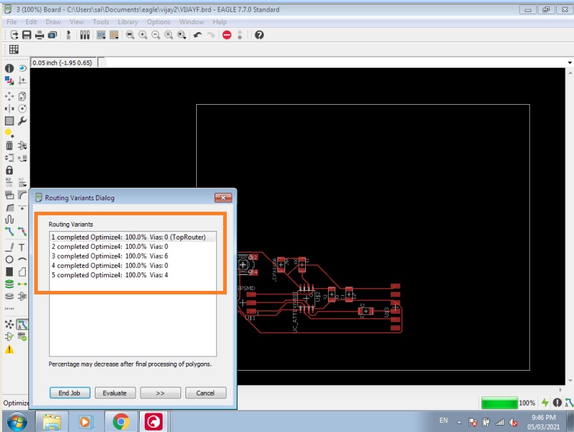
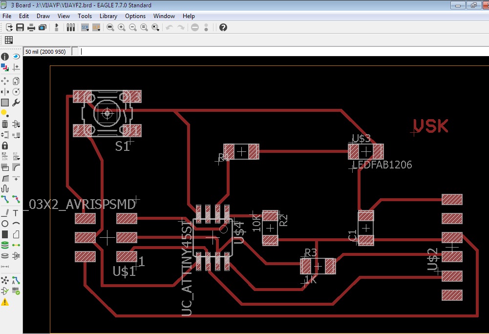
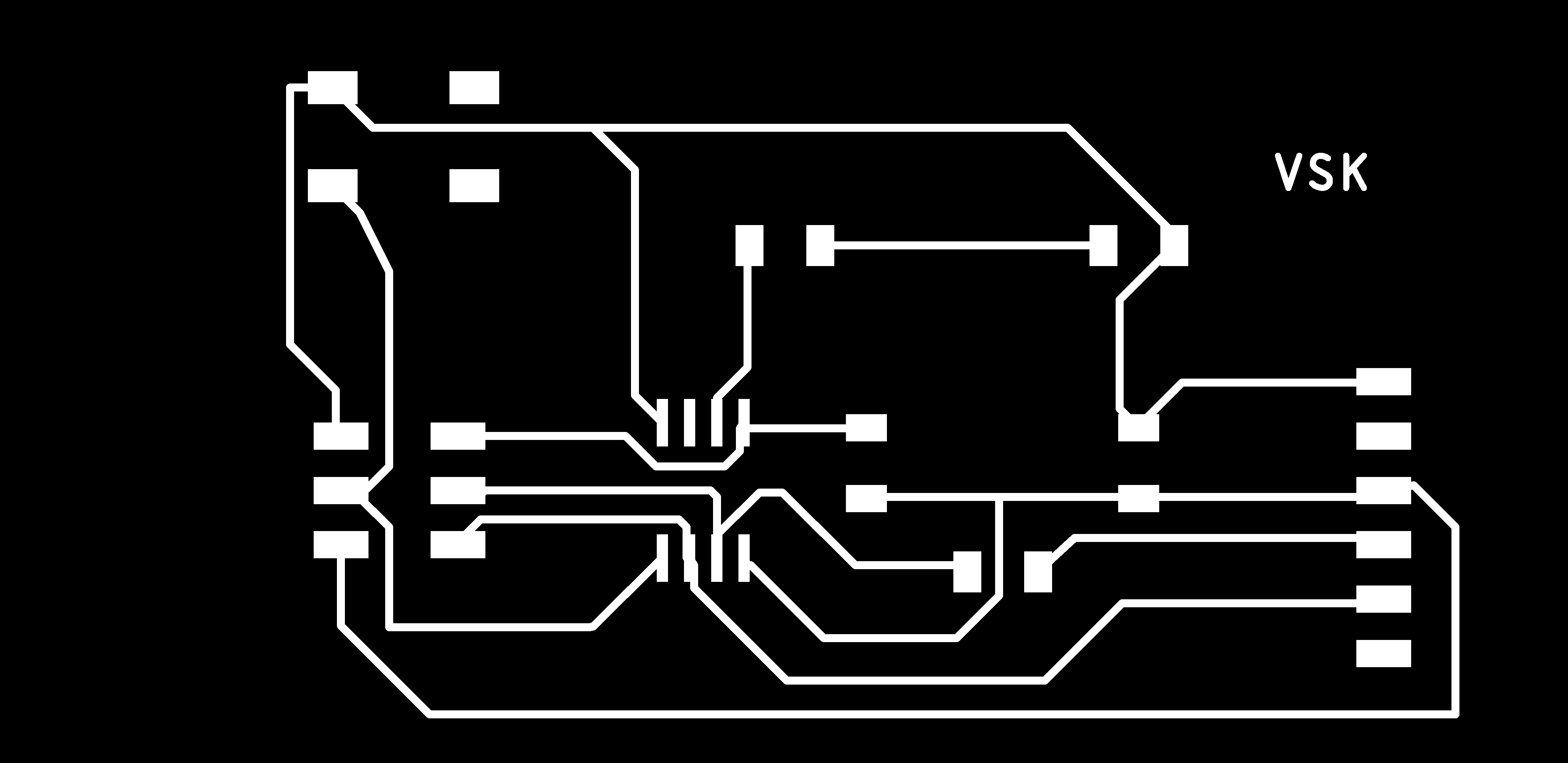
After compliting the autorouting the PCB looks like
for more parctice i have aslo tried for hand routing my PCB board
By Clicking on Hand routing Option
For hand routing arrange all the components on the layout. Click on rout airwire. Arrange all the route one by one such that two connecting wires cross does not connect each other.
for more parctcie
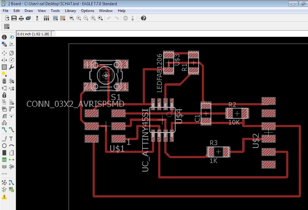
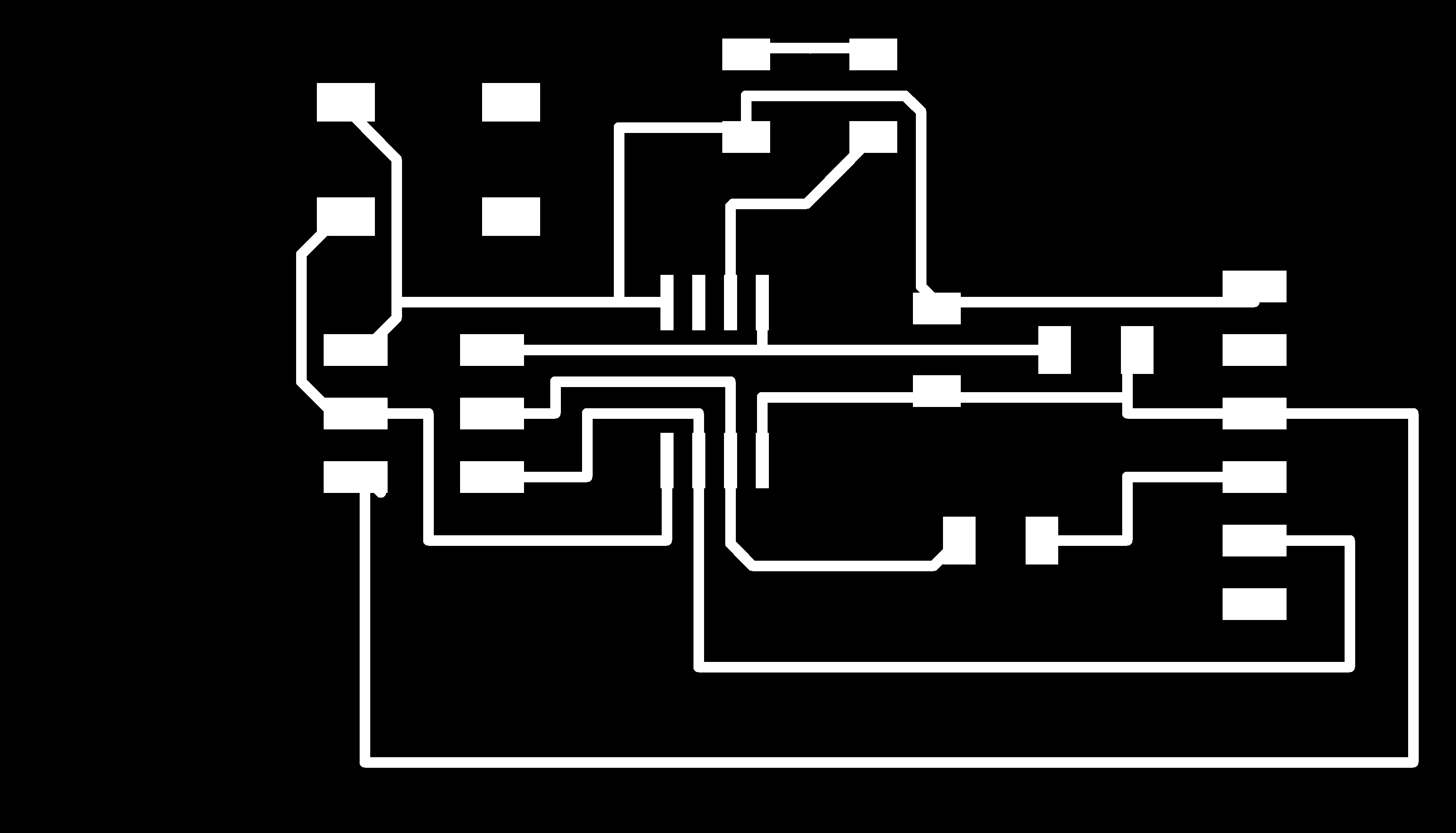
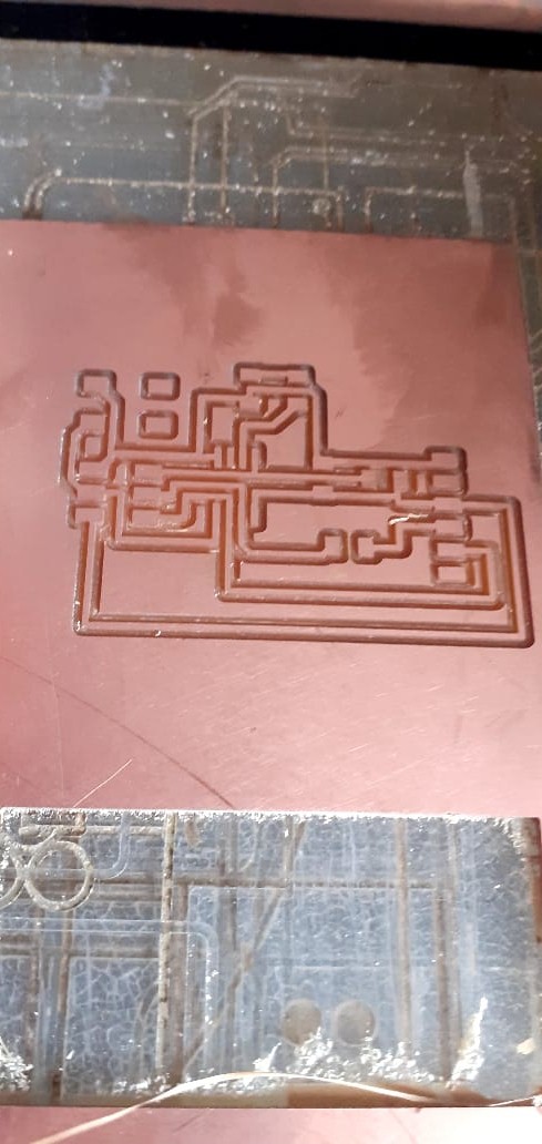
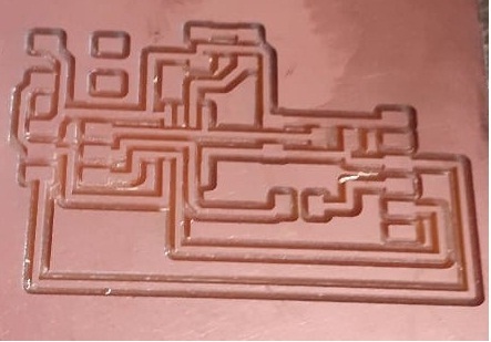
This is handrouted PCB Board
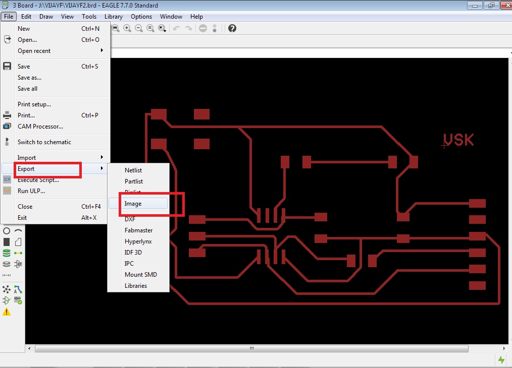
After compliting routing i had to go for exporting my board as a .png format.
first i need to remove all unwanted layer except top layer, go to view menu ->> layer setting applied layer setting and click on ok.
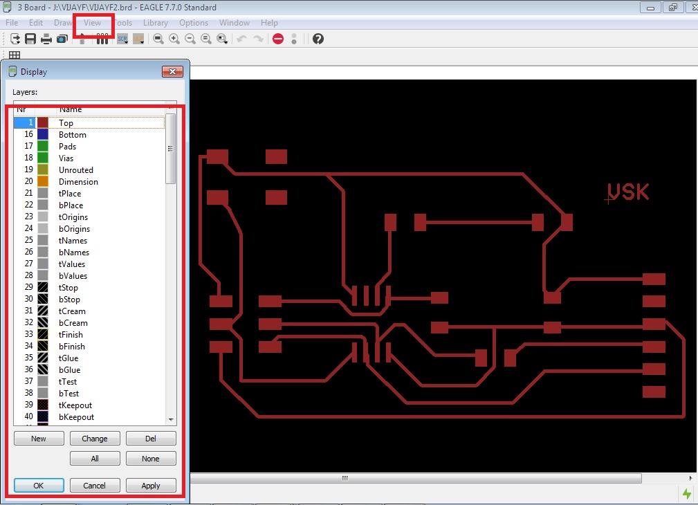
Then go to file menu export image as .png format, give the extention that you want to save your file, chage the dpi , and click on monochrome
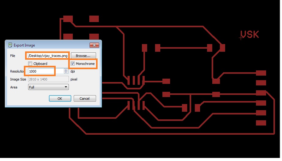
similarly, by removing top layer i got the cut out image and save it by .png format
This is the final png image for milling
Hand Router Cut Traces image in .png format
PCB milling by SRM-20 machine:
Initially I prefered Handrouted Design Used for Milling
For milling the PCB Board , again i need to go for mods server so that i ca complete my milling process.
1) First connect the server properlly.
2)Then select png image from files.
3) set the required parameter on bash mods window.
4) Select the tools (For trace 1/64 inch tool and for cut 1/32 inch tool) and click on calculate.
5) set the X,Y,Z axis as per requirement
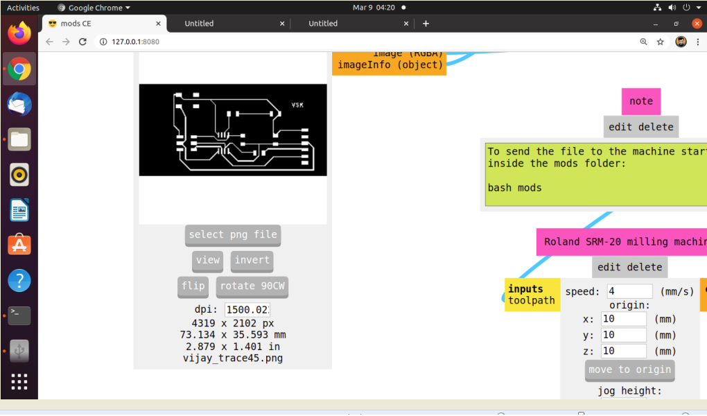
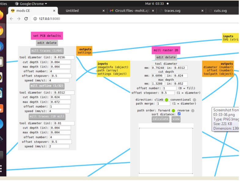
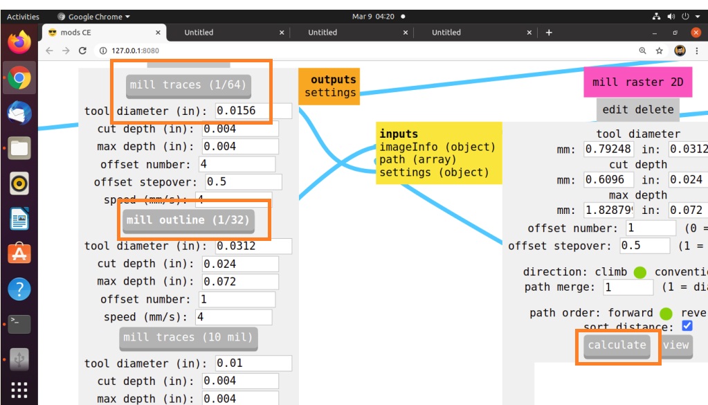
After setting all parameter sent my file to mahcine
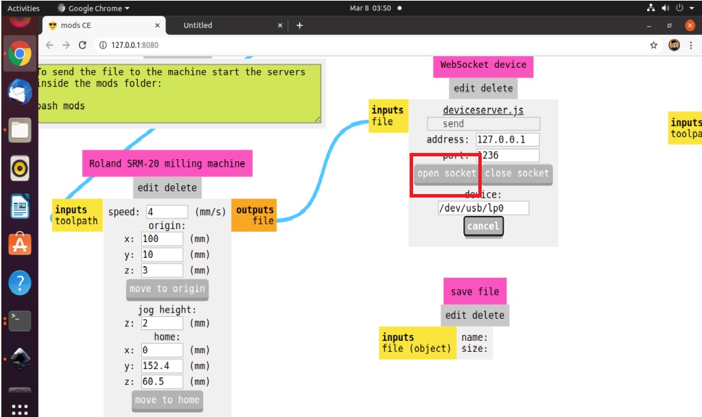
PCB milling processing by SRM
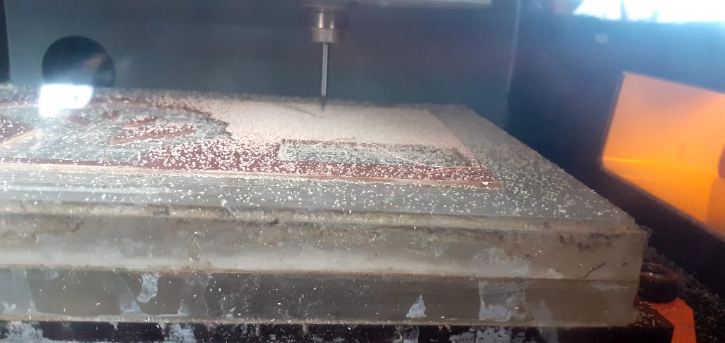
After completing the milling process my PCB board is ready
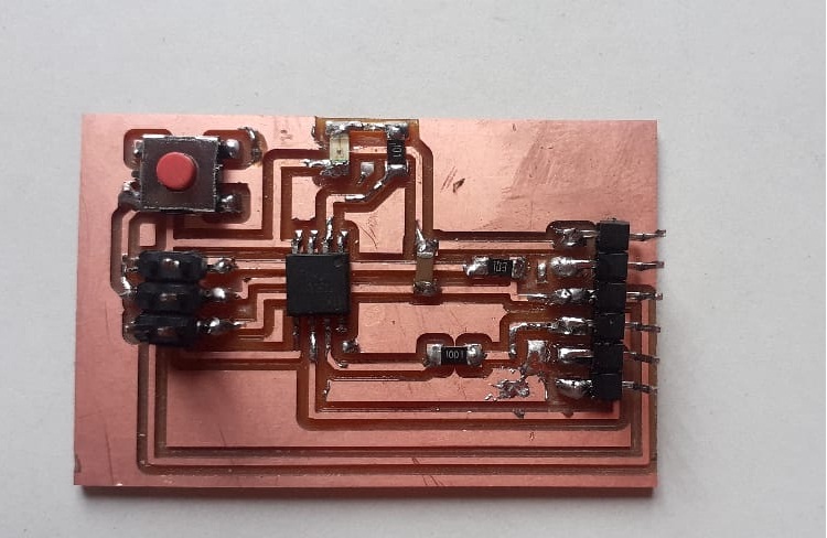
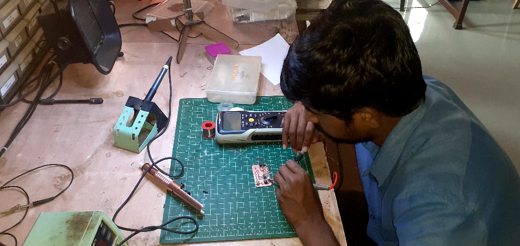
Now, I had to go for selecting and soldering the component on PCB Board
By reffering the Fab academy websites i have select the required component for attiny45 microcontroller board
1. Capacitor 1 Nos.(1uF)
2. Resistor 2Nos.(10K,1K)
3. AVRISP-smd Connector 1 Nos.
4. FTDI-SMD Header connector 1 Nos.
5. Attiny45 Microcontroller IC 1 Nos.
6. LED.with Resistor (1.8 V/0.01amp=180 ohms, 100 ohms available in our lab. 1 Nos)
7. Button 1 Nos.
After that this all component soldered on PCB
Then i need to check the connections and Conductivity of the PCB Board :
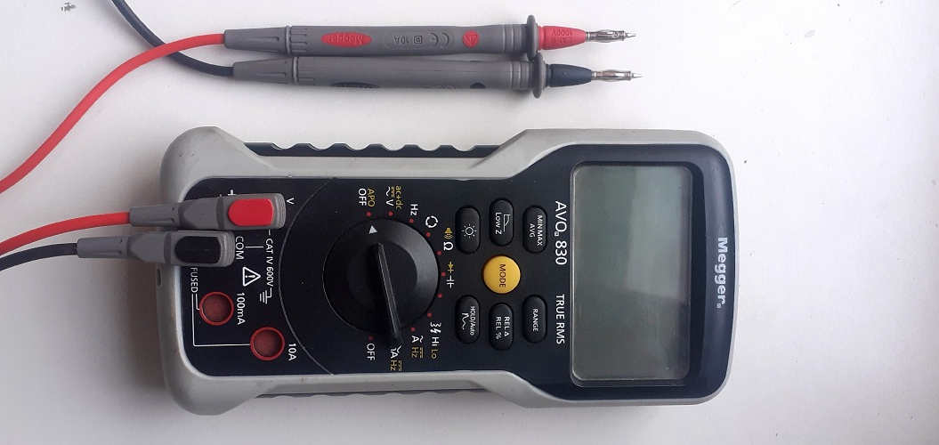
The conductivity of the board is checked by using Megger Make Multimeter
Programming and testing The Attiny45 Board.
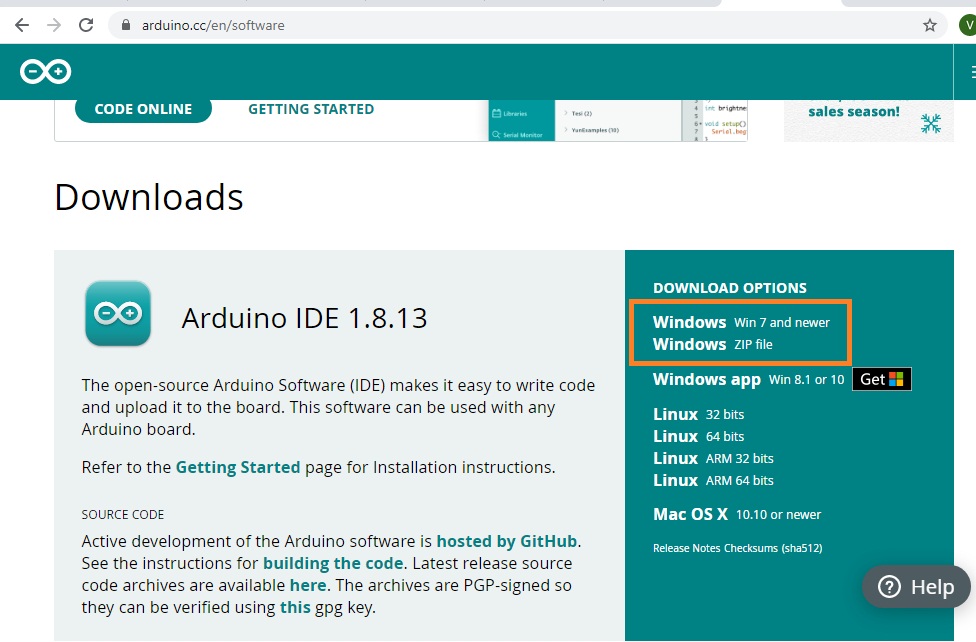
For programming ATtiny 45 first i have downloaded the Arduino Software form website
Download and install the latest Arduino Arduino IDE software link Link
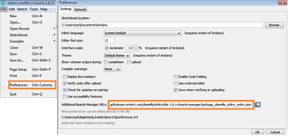
By default Arduino IDE doesn't support ATtiny45 so we should add ATtiny boards to Arduino IDE. At first you should go to File/Preferences and copy this link:
Attiny45 Board DOWNLOADED FROM THIS LINK
OR We can follow the below steps also for updating the board package of Attiny45
Go to Board maneger menu and installed the required Board package i.e. Attiny45 just by entering Attiny45, and then installed this
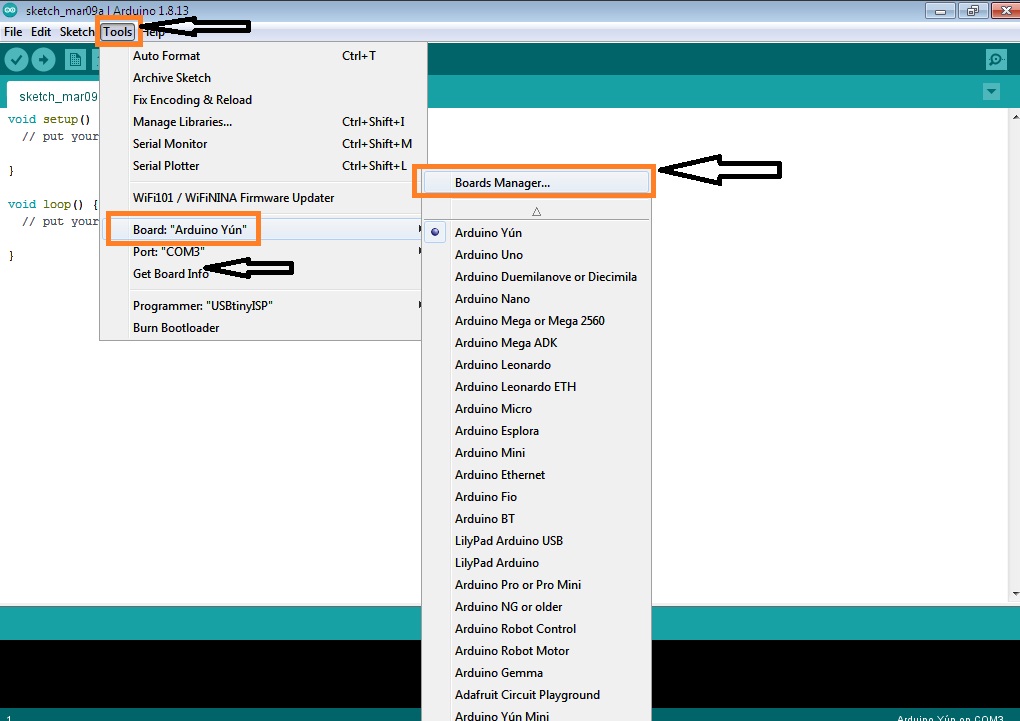
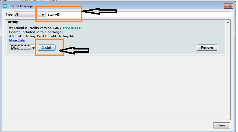
Then you will be able to see the attiny availble in the list
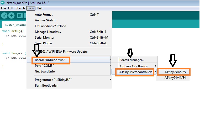
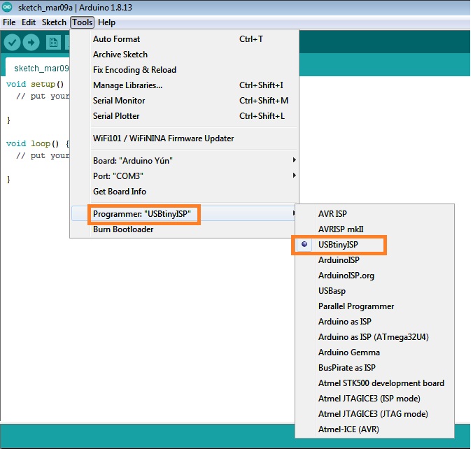
Then go to Programmer select USBtinyISP
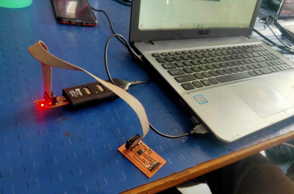
Now, i have to checked where my board working or not
1) first i have taken the FabISP which is already programmed in electronics Production week assignment.
2) connect FabISP with attity45 PCB hello world board to AVRISP conector.
3) Open the Arduino softWare
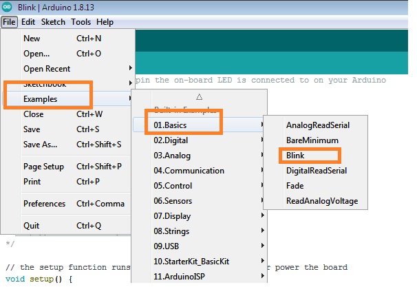
4) Go to Example in example go to blink programme which is readely available
5) open the program and edit it
6) As I have connneted LED to Pin number 3 , so by making required chenges in the program and upload the program in attiny45 Microcontroller Board
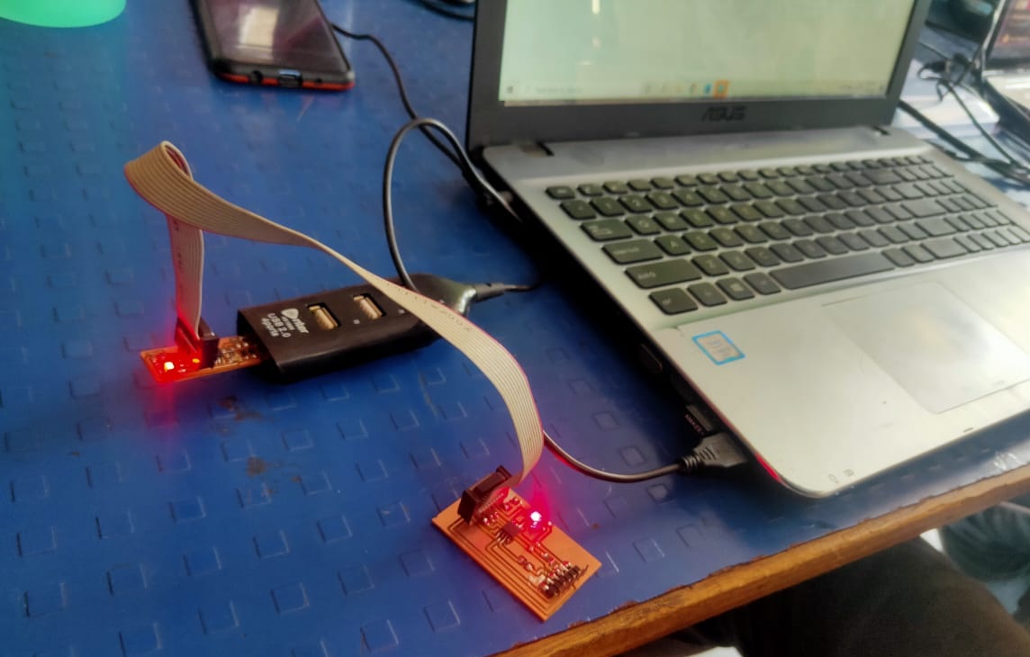
7) But, here I have faced one problem the LED was not bliking.
8) Again i have rechecked all the connection and found that LED connected to board was opposite in polarities
9) Again i have desolder and solder LED by changing its polarity .
10) Then followed the same step and observed that LED was blinking, So In this way attiny45 Microcontroller Board Programmed sucessfully.
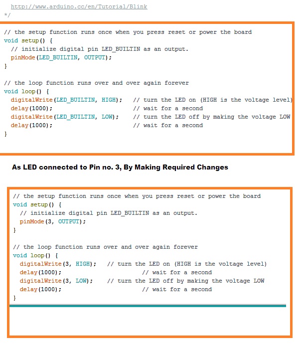
As I said the led Connected to pin. number 3 of my attiny 45 board Images Shows the LED as Bliking after uploading the program
This is the video Shows, that LED is Blinking which is connected to pin number 3.
sAbout Group Assignment
In this week of group assignment we have tested the electrinics equipment like Multimeter,DSO(Digital Storage Oscilloscope.
So we have tested the above devices one by one and Observe the characterstics available in our fablab at vigyan ashram
and observed the operation of Microcontrooler Circuit board
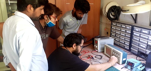
Equipment need to be tested
1) Digital Multimeter
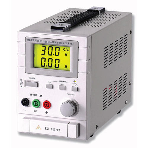
2) Regulated Power Supply
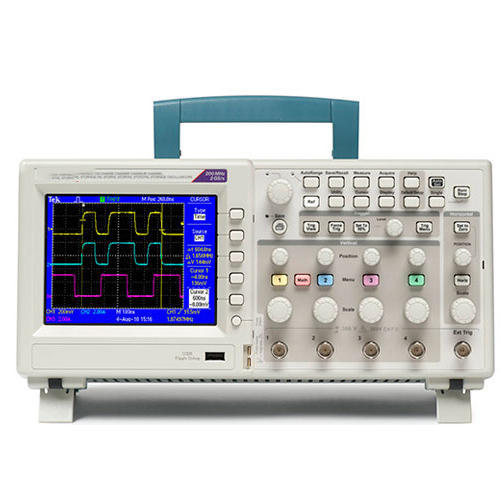
3) Digitital
1. Digital Multimeter:
A digital multimeter is a test tool used to measure two or more electrical values—principally voltage (volts), current (amps) and resistance (ohms). It is a standard diagnostic tool for technicians in the electrical/electronic industries.
2. Regulated Power Supply
Its function is to supply a stable voltage (or less often current), to a circuit or device that must be operated within certain power supply limits. The output from the regulated power supply may be alternating or unidirectional, but is nearly always DC (Direct Current).
2. Digital Stoarage Oscilloscope
The digital storage oscilloscope is an instrument which gives the storage of a digital waveform or the digital copy of the waveform. It allows us to store the signal or the waveform in the digital format, and in the digital memory also it allows us to do the digital signal processing techniques over that signal. The maximum frequency measured on the digital signal oscilloscope depends upon two things they are: sampling rate of the scope and the nature of the converter. The traces in DSO are bright, highly defined, and displayed within seconds.
The details about Group Assignment
Click here to detail about Group Assignment
What Problems I have faced
1. While drawing the desing of board through eagle software net lable should be proper otherwise its gives the Errors.
2. I have faced one more problems when the DRC Rules are not properly set then the width of traces are not proper, so again i had to change the DCR rules
What i have learned?
1. I have learned ,How to use the Eagle Software for circuit board design
2. Various Elecronics Component used in Electronics Circuit
3. Specification and selection of components for circuit
4. Microcontroller and its pin configurations.
5. Machining, soldering and conductivity testing of board
6. Testing of Microcontroller Board Through Arduino Programming
7. To test the microcontroller using different test equipment such as regulated power supply, digital multimeter and oscilloscope.
DOWNLOAD's
Download my original file here