Electronic Design
Making of Hello! Board
Intro.
Hey! welcome to my weekly assignments. This week is for electronic design where I make my own Hello! board and fun circuit to explore and practice skill.
.jpg)
Week Task:
Group assignment: use the test equipment in your lab to observe the operation of a microcontroller circuit boardIndividual assignment: redraw an echo hello-world board, add (at least) a button and LED (with current-limiting resistor) check the design rules, make it, and test it extra credit: simulate its operation
Group assignment: Summary
So while making a board on each step we all already testing our board continuity to make sure in not got short on any point and all connection are properly made. All by using multimeter. In group we test out board one with variable power supplier to findout how much current board is consuming and another test out with DSO ( Digital Storage Oscillator ) to see waveform board was generating.
Individual Assignment:
about Electronic
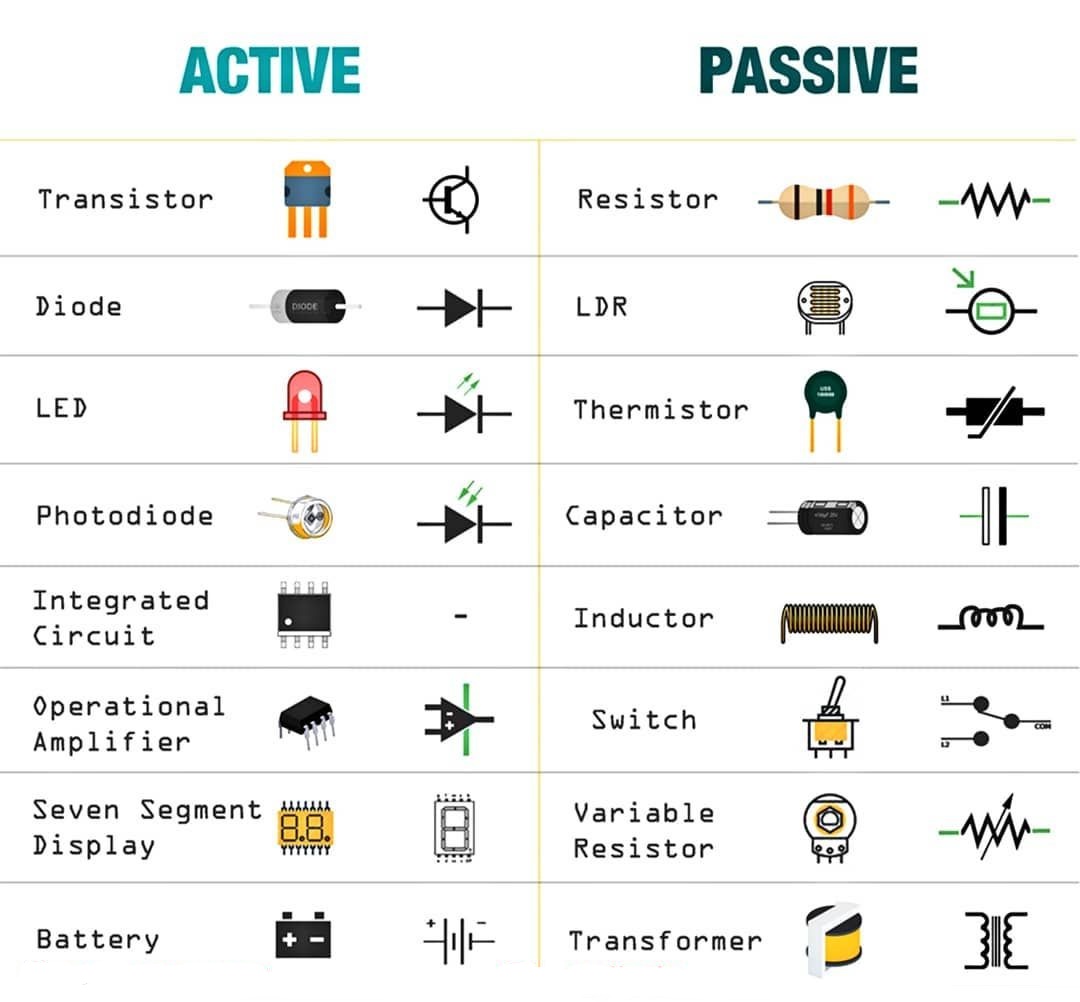
Electronics is the study of how to control the flow of electrons. It deals with circuits that are made with parts called components and connecting wires that control the flow of electricity and direct it to do useful things.wikipedia
Electronic components
An electronic component is any basic discrete device or physical entity in an electronic system used
to affect electrons or their associated fields.
Active components rely on a source of energy (usually from the DC circuit, which we have
chosen to
ignore) and usually can inject power into a circuit, though this is not part of the definition.
Active components include amplifying components such as transistors, triode vacuum tubes (valves),
and tunnel diodes.
Passive components cannot introduce net energy into the circuit. They also cannot rely on a
source
of power, except for what is available from the (AC) circuit they are connected to. As a consequence
they cannot amplify (increase the power of a signal), although they may increase a voltage or
current (such as is done by a transformer or resonant circuit). Passive components include
two-terminal components such as resistors, capacitors, inductors, and transformers.
wikipedia
Integrated Circuit
An integrated circuit (also referred to as an IC, a chip, or a microchip) is a set of electronic circuits on one small flat piece (or "chip") of semiconductor material that is normally silicon. The integration of large numbers of tiny MOS transistors into a small chip results in circuits that are orders of magnitude smaller, faster, and less expensive than those constructed of discrete electronic components.wikipedia
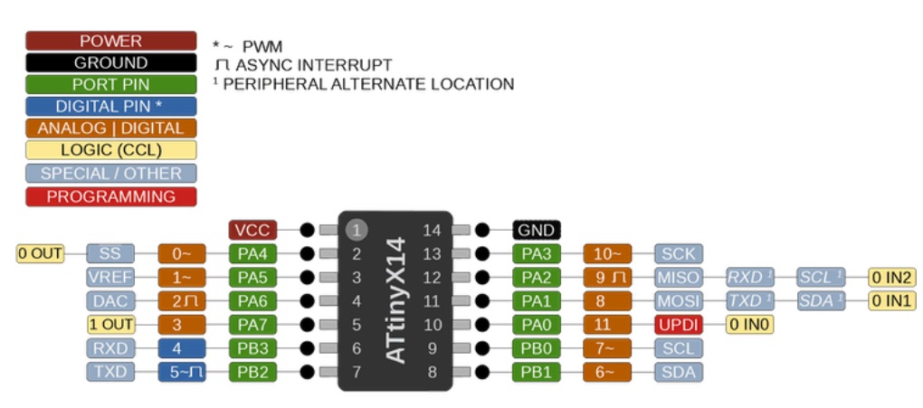
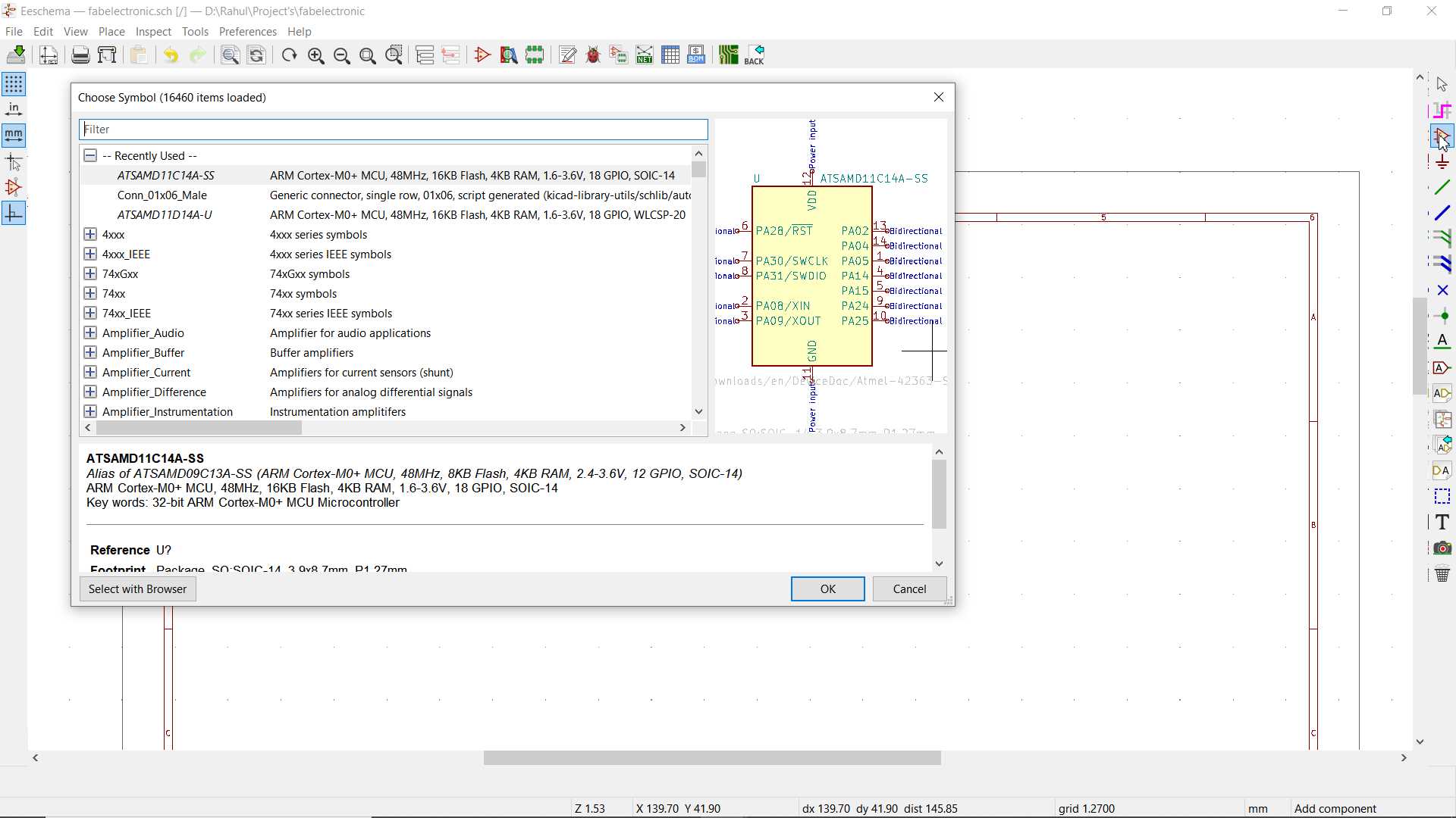
In my assignment I use programmable IC Attiny1614 in my board. Below image is a pinout attinyx14
family. as you see pin 11 is tag as UPDI that we need for programming the chip through our made UPDI
programmer. Top two pin which label as VCC and GND are pin for supplying power to chip. Attiny1614
work good on 5 V. DC supply.
So I was planning to make something new in a new way like wanna to explore new software, new component and new type of PCB like flexible or cloth one
Since I had one week to do assignment I decide to first do what is need for completing task and afterward if get time I will do more creative things
In my electronic production week I have made two programmer FabISP and UPDI programmer. since I have used ISP progrmmer before so I choose to work on UPDI one now
This week I will build my own board that can be program using UPDI pin.
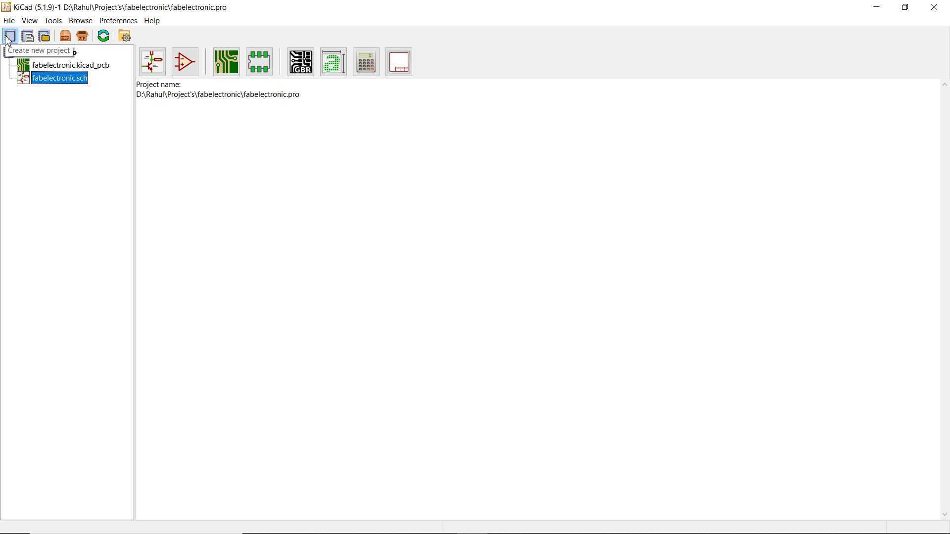
For circuit designing I used KiCAD and for printing board in going to use milling process.
KiCAD
kiCAD is open source electronic schmetic and pcb designing software.
Getting Started
Download and install in your pc
Run it and thats how it look . create new project and let begin with schmetic design on left panel. double click to open it
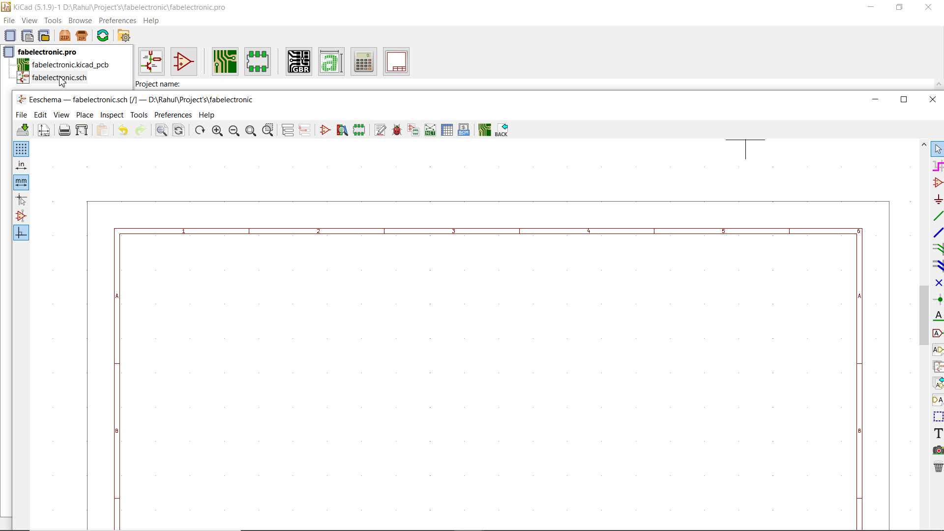
On right side of Kicad schmetic designing layout you will find toolbar we mostly going used those while designing
Before moving to anything let also install fablibrary where you will find most of components and headers to work on.
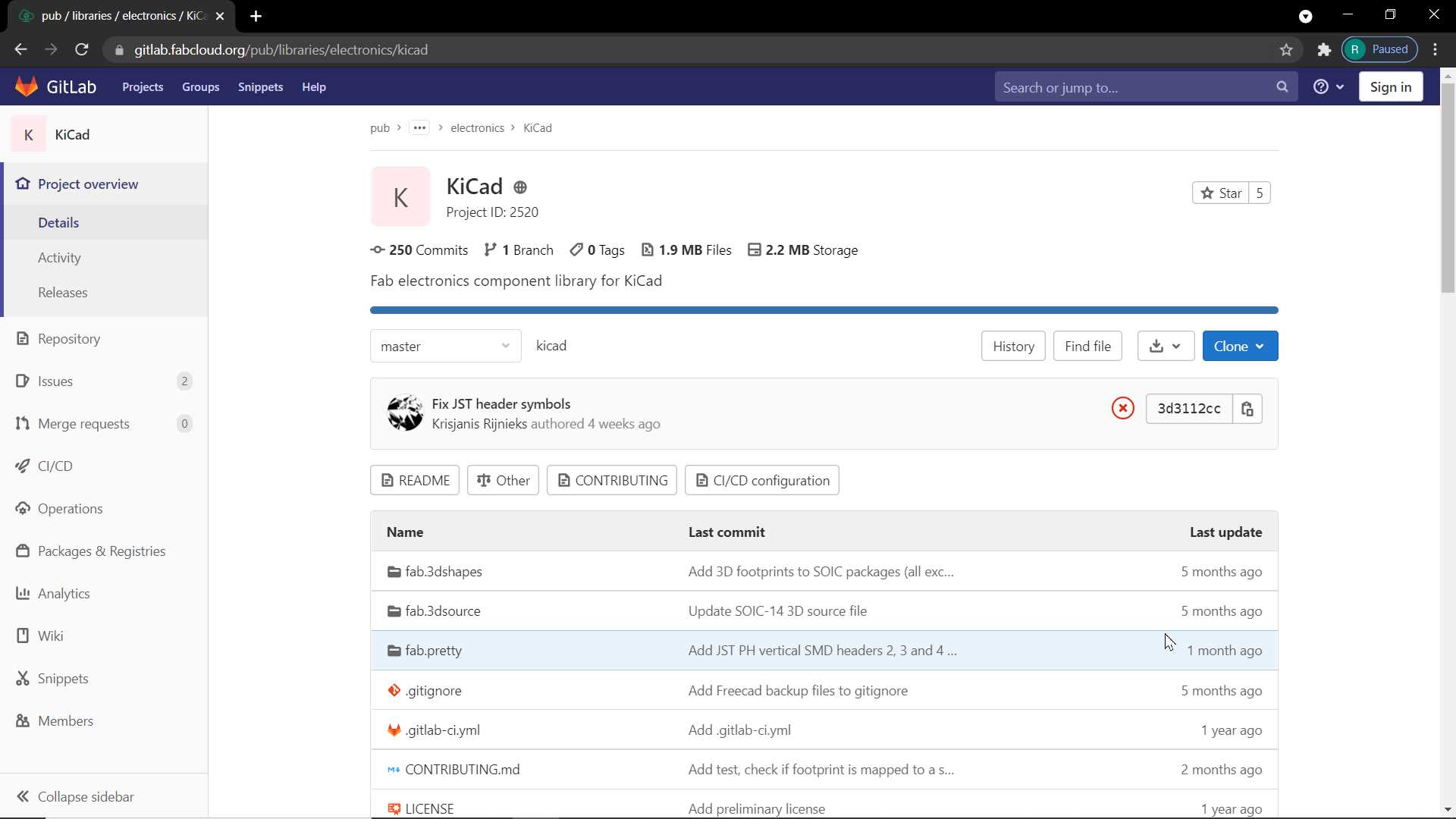
Clone or download this repository. You may rename the directory to fab.Store it in a safe place such as ~/kicad/libraries or C:/kicad/libraries.
Run KiCad or open a KiCad .pro file.
Go to "Preferences / Manage Symbol Libraries" and add fab.lib as symbol library.
Go to "Preferences / Manage Footprint Libraries" and add fab.pretty as footprint library.
Go to "Preferences / Configure Paths" and add variable named FAB that points to the installation directory of the fab library, such as ~/kicad/libraries/fab or C:/kicad/libraries/fab. This will enable the custom 3D shapes to be found. The 3D shapes project has just started and most of them have to be populated still.
Using symbols tool placed symbols for components need on Board. since I using UPDI programmer and choose to work with attiny1614 MCU I place it symbol first and then placed other components.
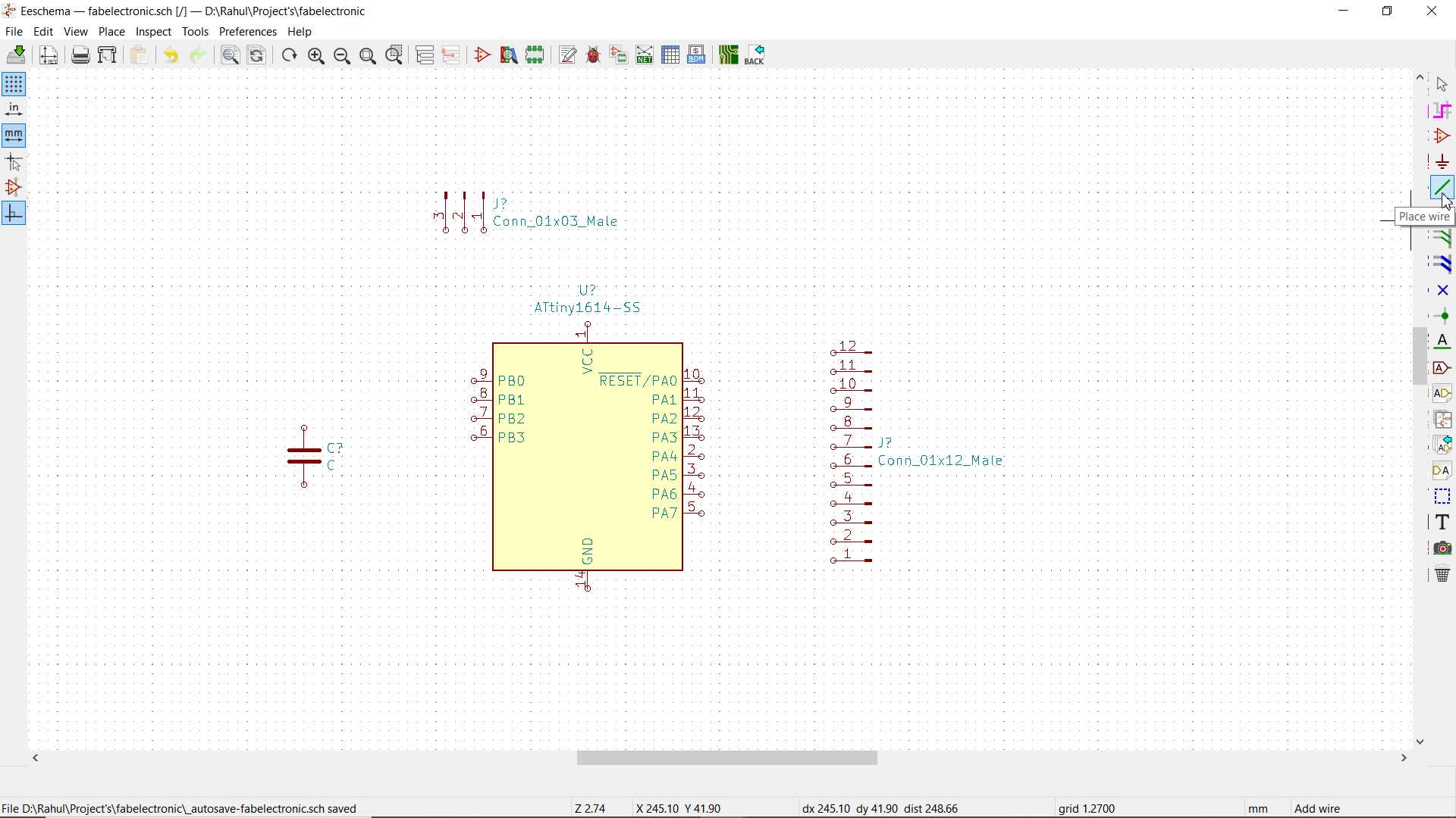
Using wires tool I made connection between placed components. I wanna to make my board for multi purpose so I took out each possible pins and connected with header so that it can be used anytime whenever is needed. This will my main board as I plan to design one another board to attach it with
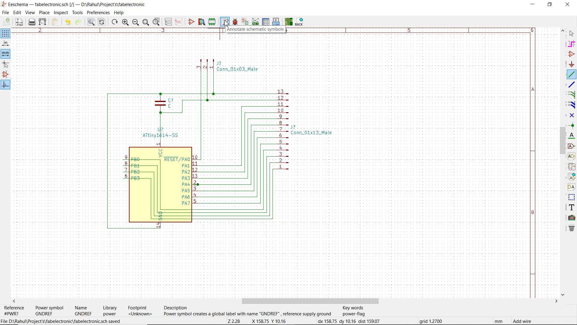
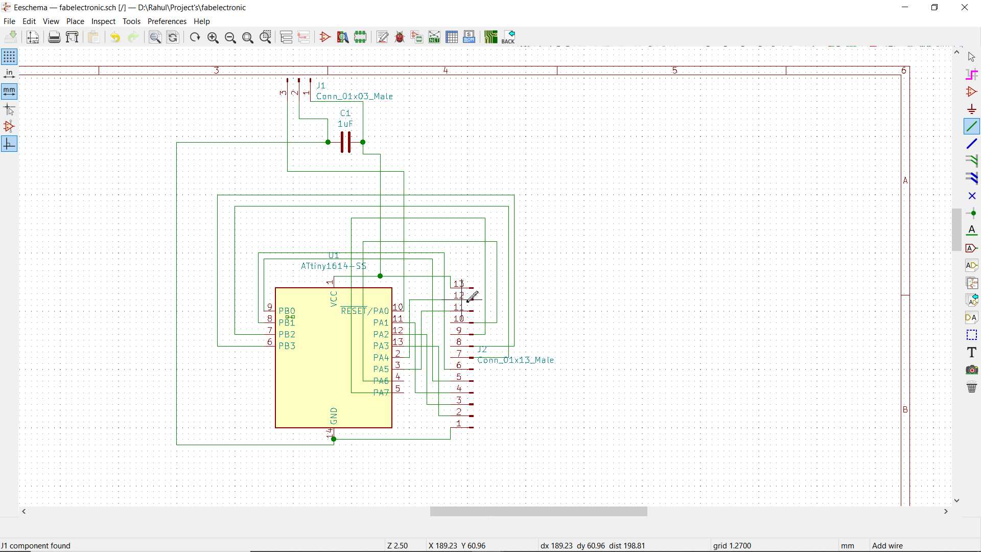
One thing I found helpful while designing pcb you have to predict how your connection will look like. Here I completed with Schmetic and ofcourse it is unmanaged but it will not affect final pcb but yes! will learn to design proper schmetic in upcoming days.
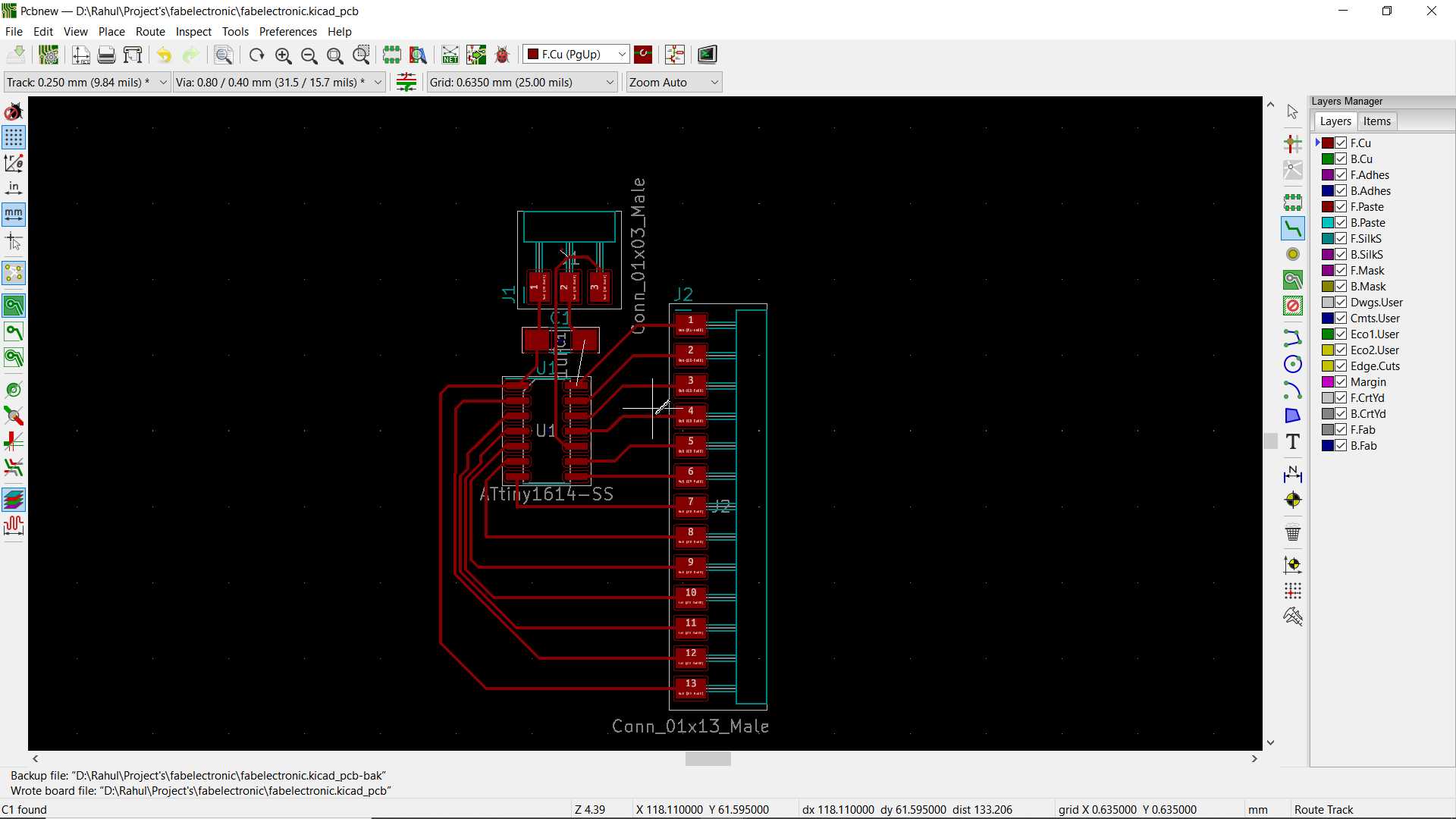
Okay so move on to pcb designing . In kicad before moving to pcb desiging layout we first need to give Anotation, Assign PCB footprint for components been use and last needed to Generate netlist file
Run PCB layout and In PCB layout window there is a option to load netlist which will
import your schmetic and connections in PCB layout window
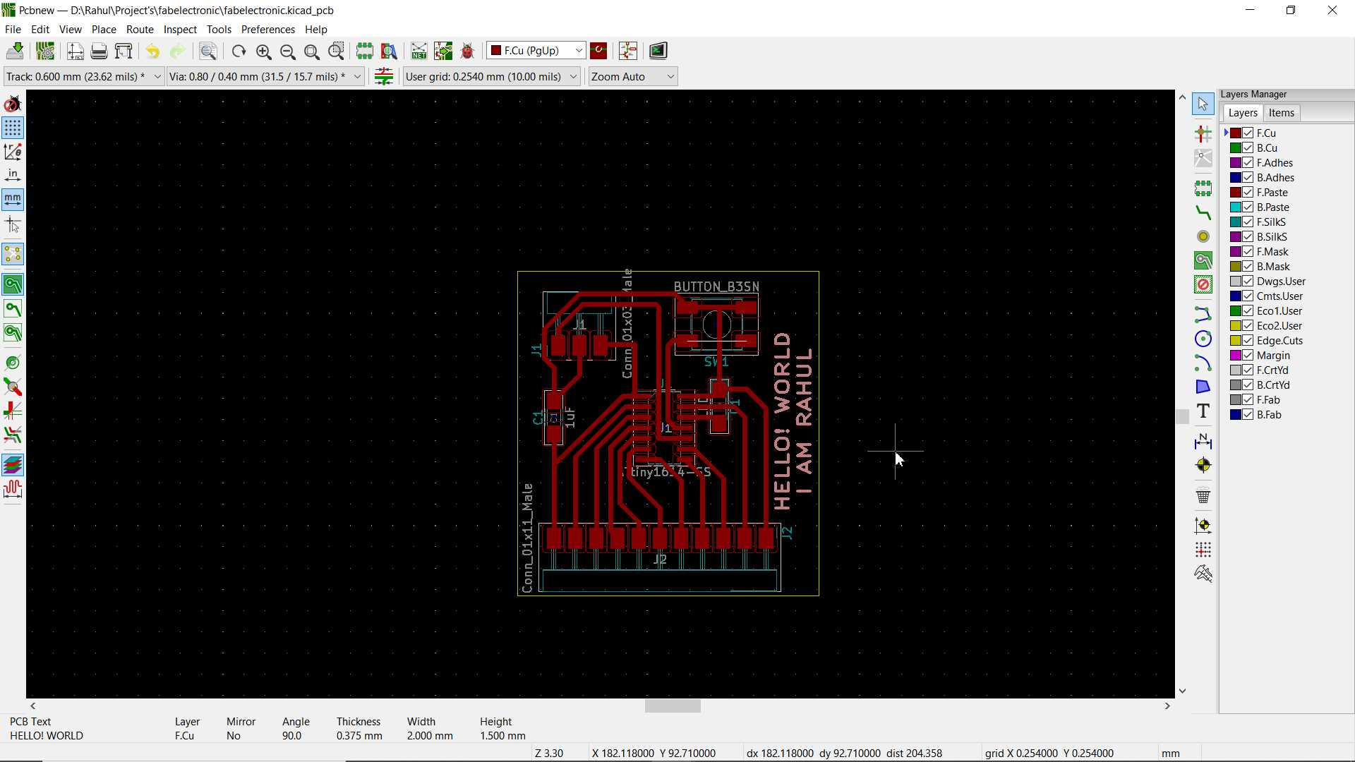
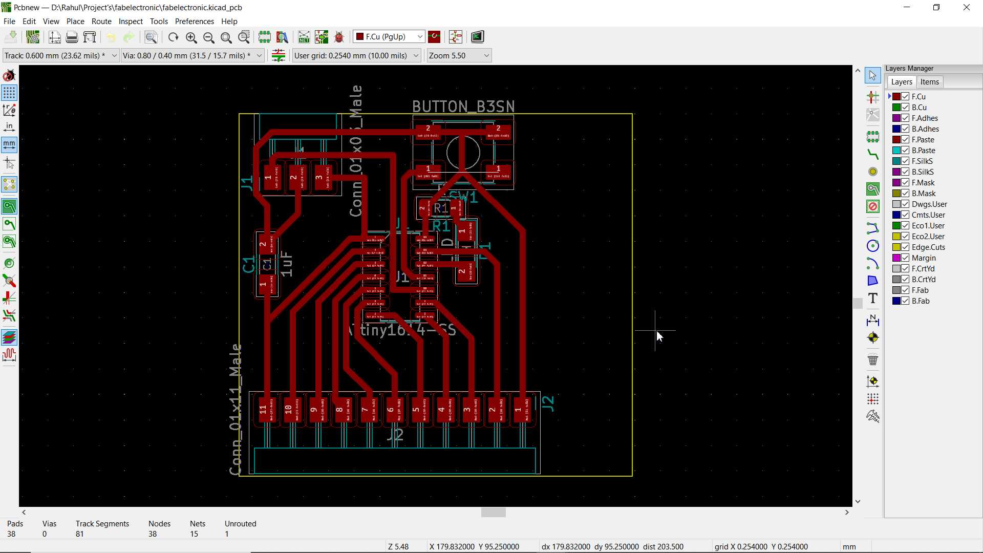
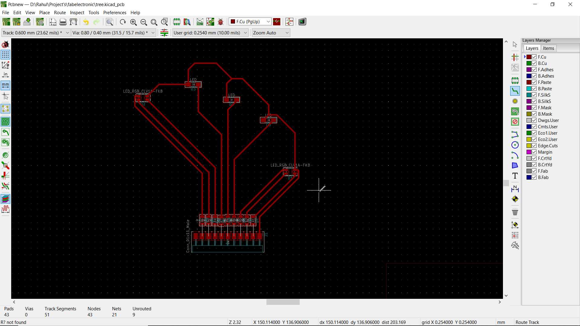
Since i have used eagle so I found here in kicad there is no auto route option so we need to make route manually and as you see I tried it multiple time until I get satisfied to something
So some more experiments and arrangements and it turn into this
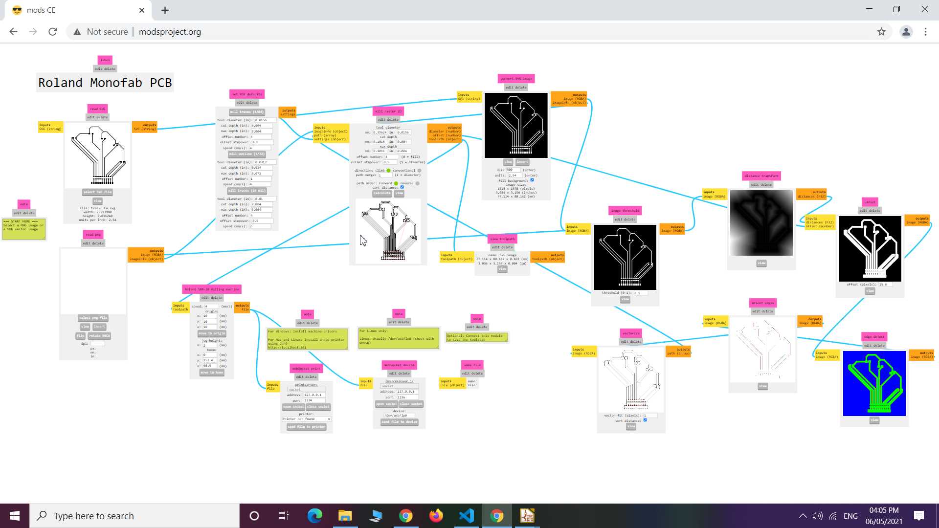
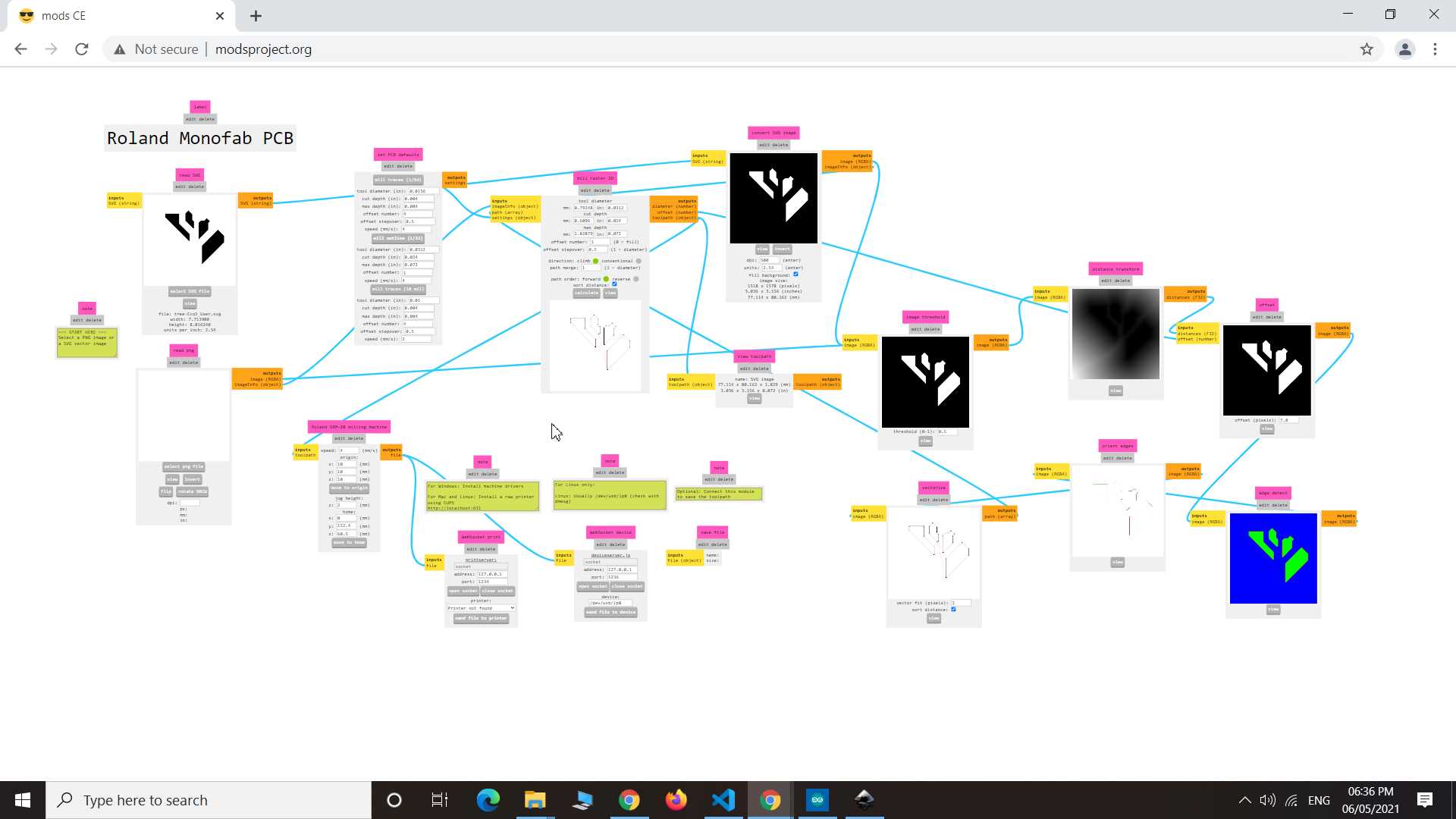
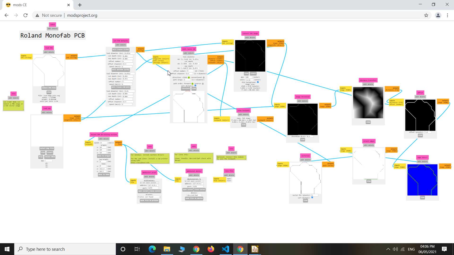
Exported design into svg and using mods Milled it on SRM 20
.jpg)
.jpg)
.jpg)
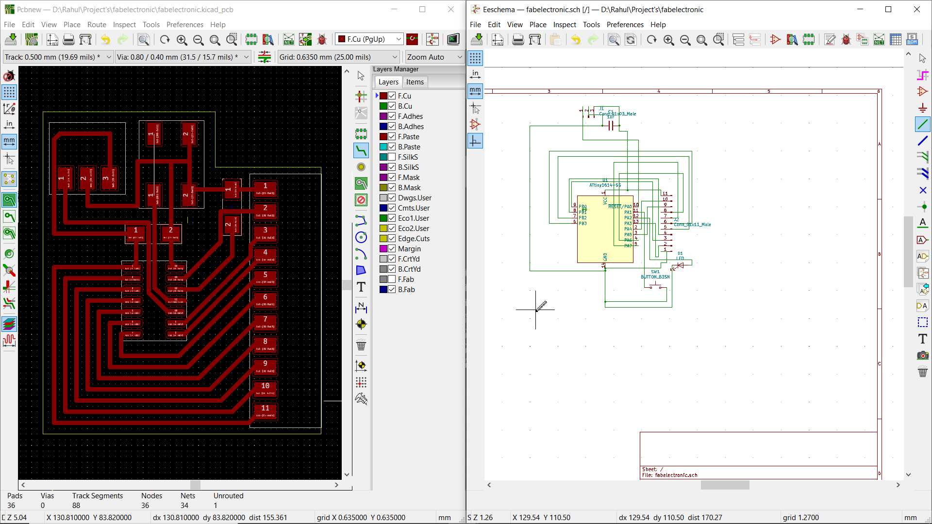
After everthing done well I found that I forgot to add resistor between led and MCU since board function on 5 volt and led require less.
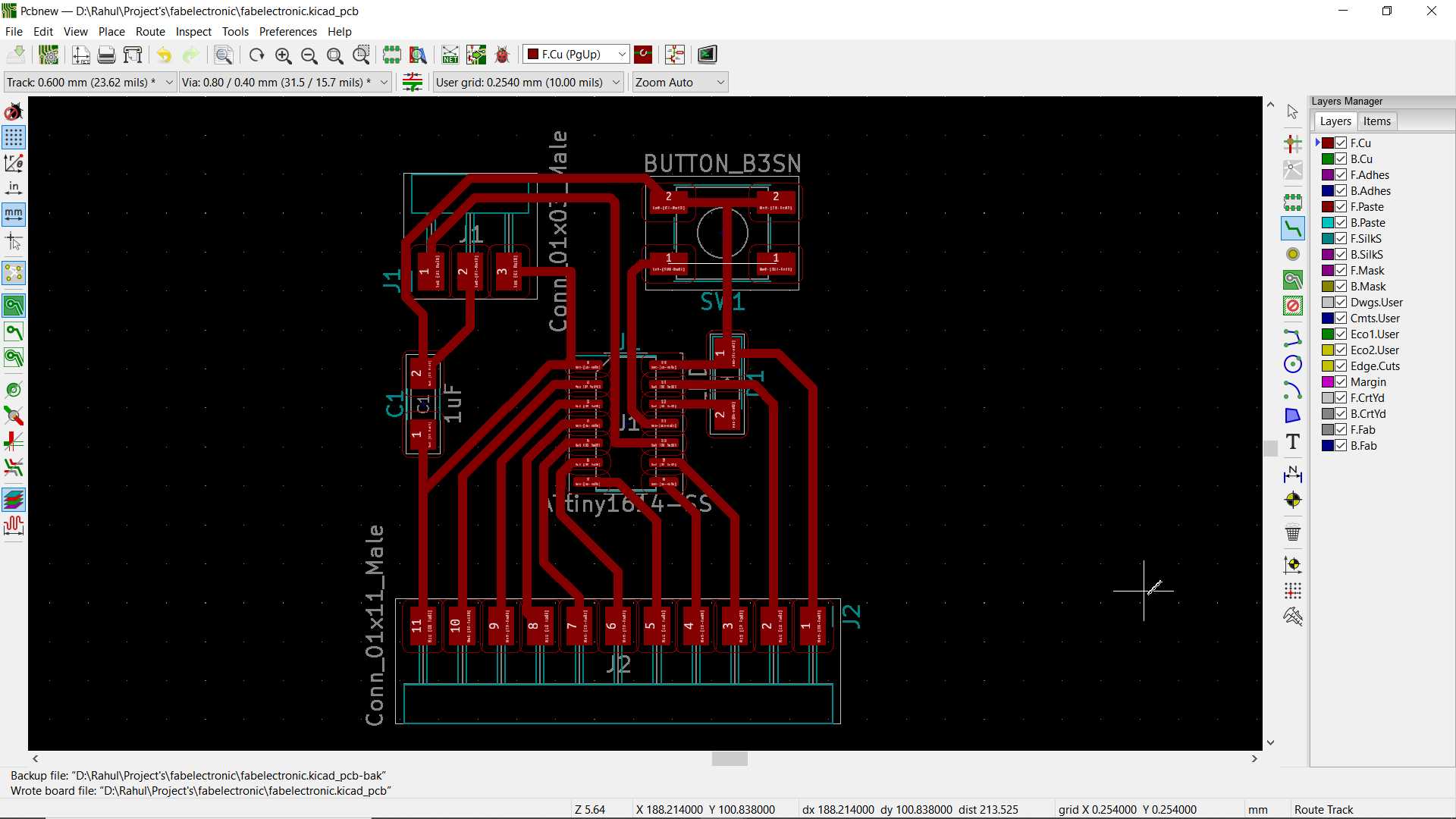
Edited and improved the design again and after little fixing here is my final design
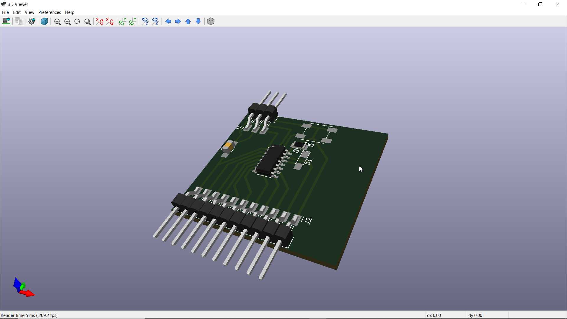
One Wonderful feature I liked is that you can Generate a 3d model view of your board that you design. This can be saved and use in while 3d cad modeling
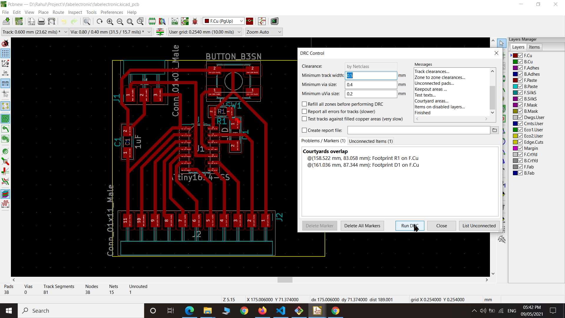
Before moving ahead I will explore one more important feature that is required to correct mistake in your design is DRC (Design Rule Check). This will detector issue in your design by comparing your given design paraments with your design
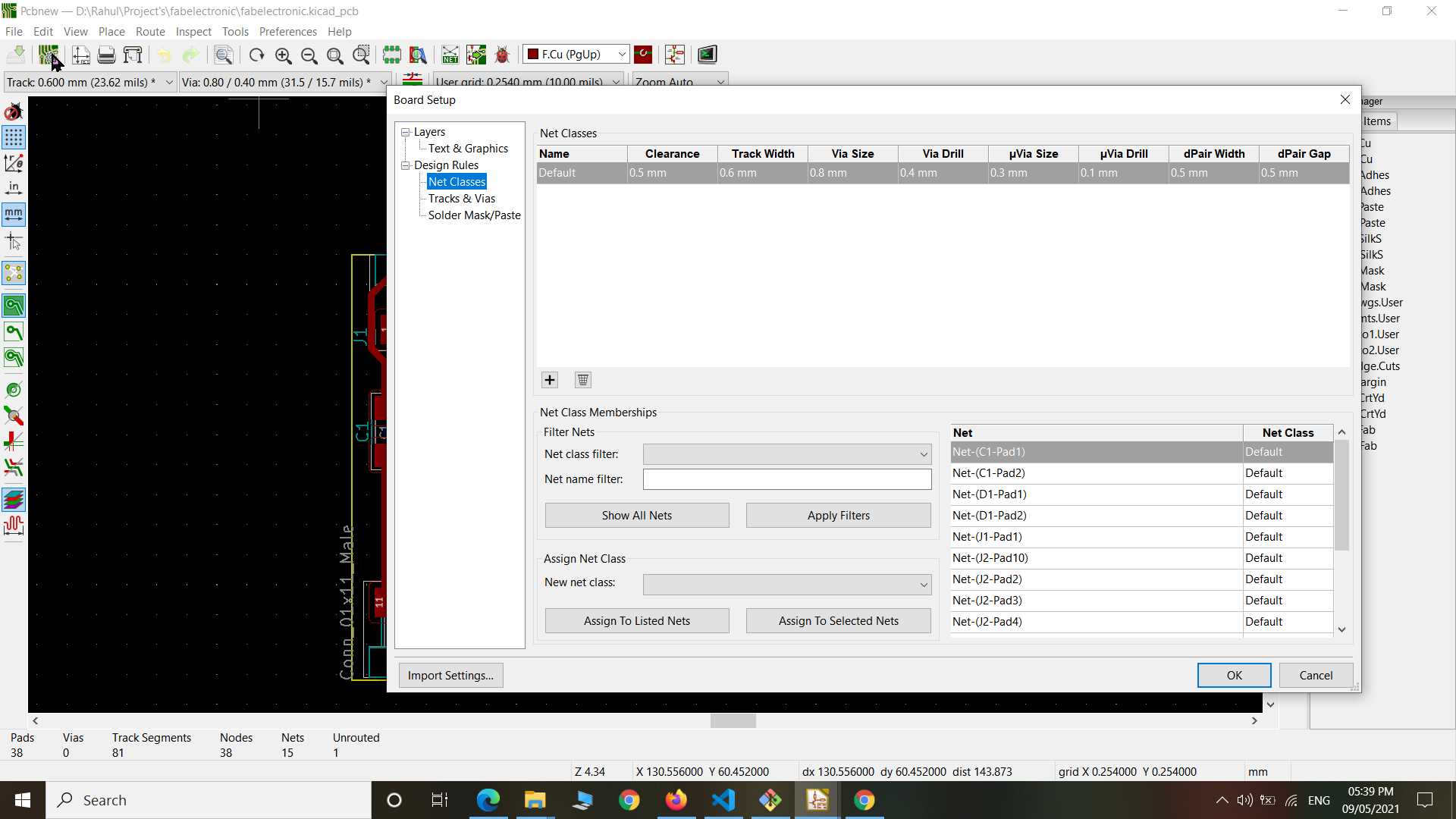
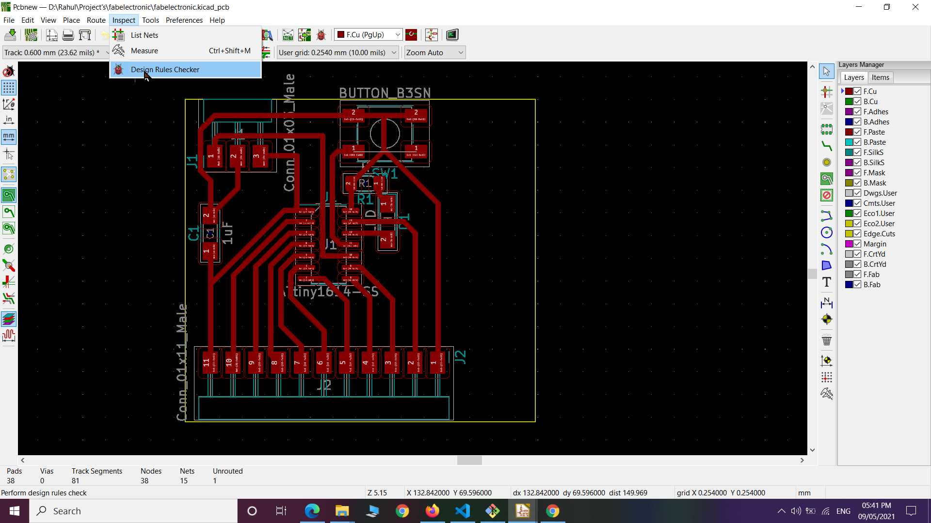
After running DRC it show some issues but that can be ignore because I am aware of that things will not bring any issue in functioning and milling. like it showing one unconnected item where i going to put push button and I know button is internally connected to that side so it will manged it. Another issue it showing is about distance between pads which also can be ignore because it already connected so if while milling it get fuse that is also fine but it actually not going to happen it just give a prediction by Calculating thing with given parameters so you just also can redefine it.
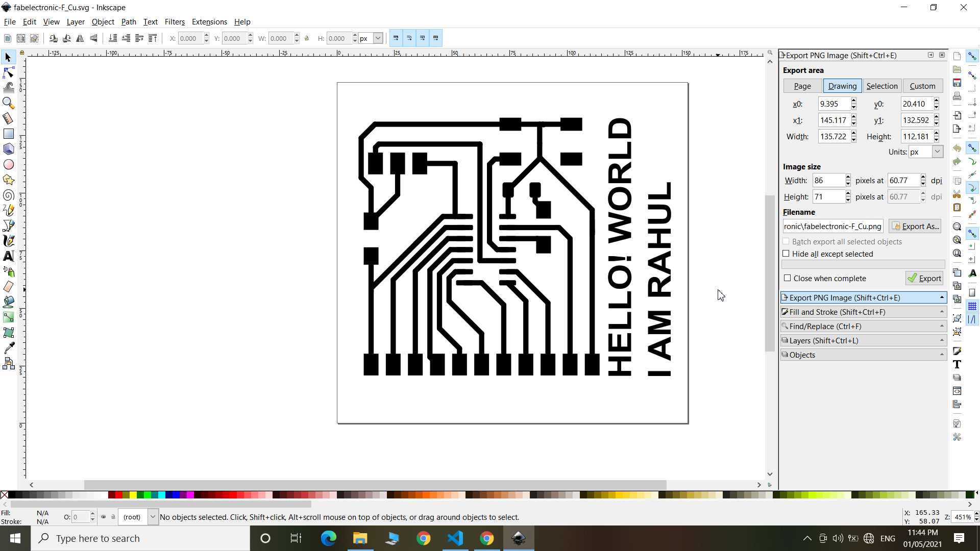
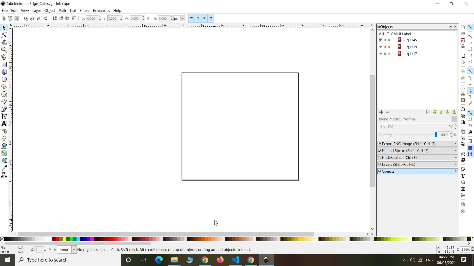
Next exported design into SVG. Remember to save different in different file here I only needed trace file and edge cut file for milling purpose. I have not add any text here now on my design in KiCAD so that I can edit it in SVG file afterward. This because last time text was not clear and font style was limited. Maybe This can be done within kicad but that time I dont know how? so I figured this way.
I opened svg in inkscape to edit and added text on it. One problem that I found in design while cutting out board that edge cut sometime failed to Generate proper path in mods. This can fixed by editing edge cut file in inkscape by reducing border by giving it inner offset if it got cut-to-cut contact to page border or else you can increase the thickness of border but it can give double cutting path.
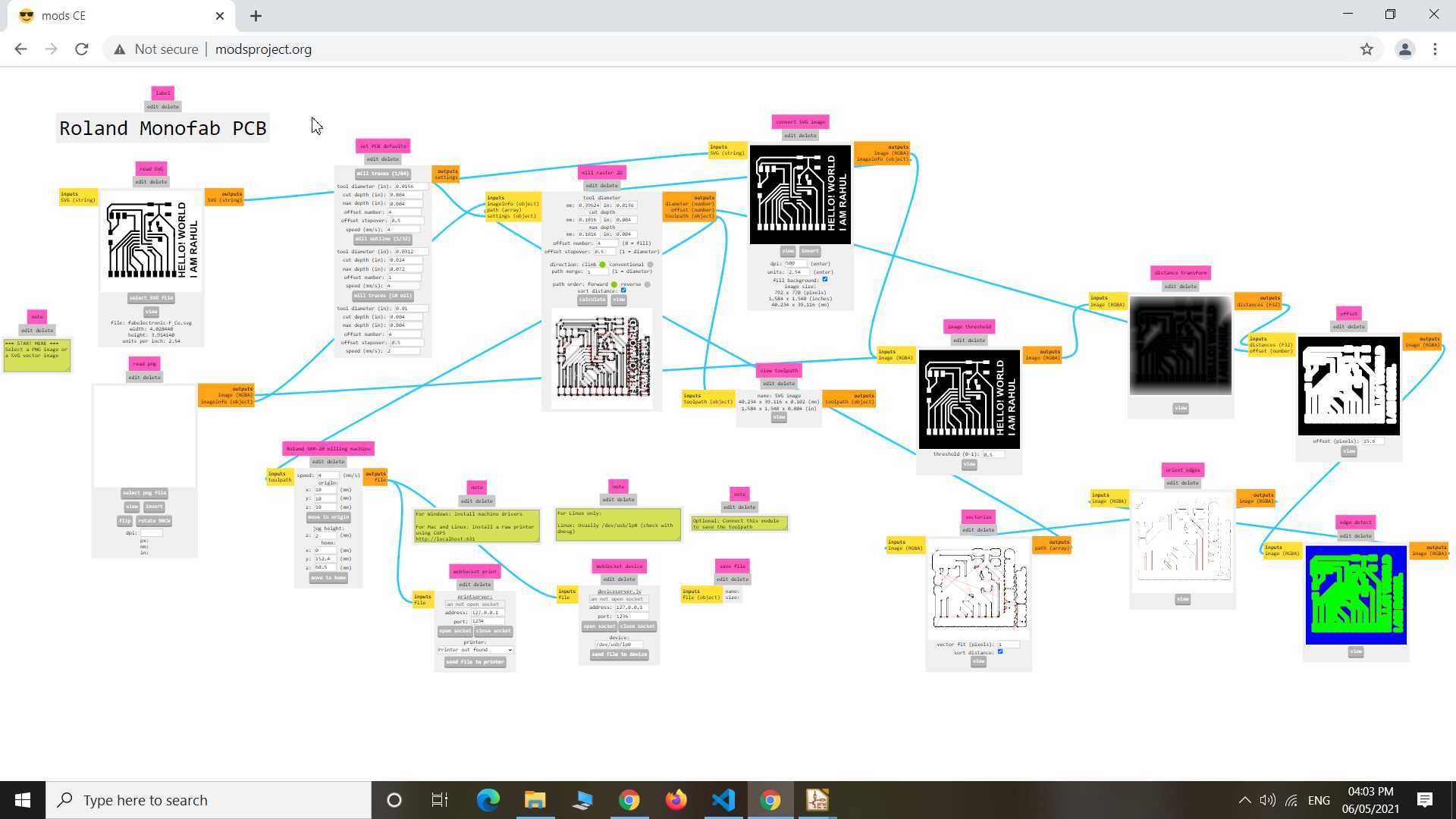
Next milled out pcb and placed all components on it
List of Components
- 1 x ATtiny1614
- 1 x Push Button
- 1 x 499Ω resistors
- 1 x blue LED
- 1 x 1uF capacitor
- 1 x Male header 1x11 pins
- 1 x Male header 1x3 pins
*Using Ohms law Calculated resistor value is 220 ohm for driving leds but because I dont have more close value resistor available here I have used 499 ohm resistor and it worked well.
.jpg)
.jpg)
So push button is connect to pin 8 and blue led to pin 9. Now time to write a code and upload it in board to test it out
const int buttonPin = 8;
const int ledPin =  9;

int buttonState = 0;
void setup() {

  pinMode(ledPin, OUTPUT);

  pinMode(buttonPin, INPUT_PULLUP);
}

void loop() {

  buttonState = digitalRead(buttonPin);


  if (buttonState != HIGH) {

    digitalWrite(ledPin, HIGH);
  } else {

    digitalWrite(ledPin, LOW);
  }
}
Verify and Upload code normally or using programmer option on arduino ide. wait of uploading get done.
So this is simple code to test my board. In video as I show on pressing button led turn on and on releasing button it turn off and that state code and board working as designed.
well done to myself :)
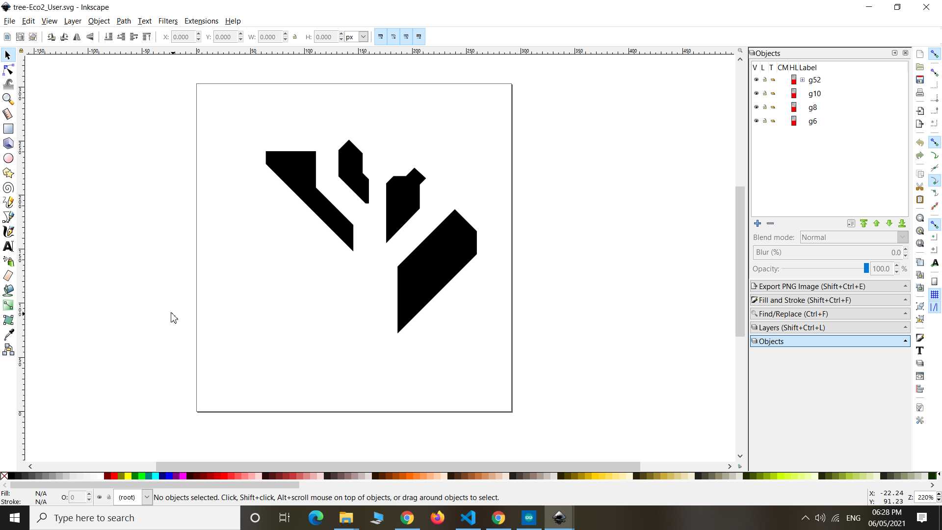
Next I started to design second board which a attachment to first board. Here in second board I not need any IC or MCU because it be control by first main board. This board just content leds and resistor to support leds. Here I experiment with pcb design. I made it like to look like tree shape and here I also used RGB leds very first time in my projects
Okay so we start with schmetic and then move to pcb. same way like before.
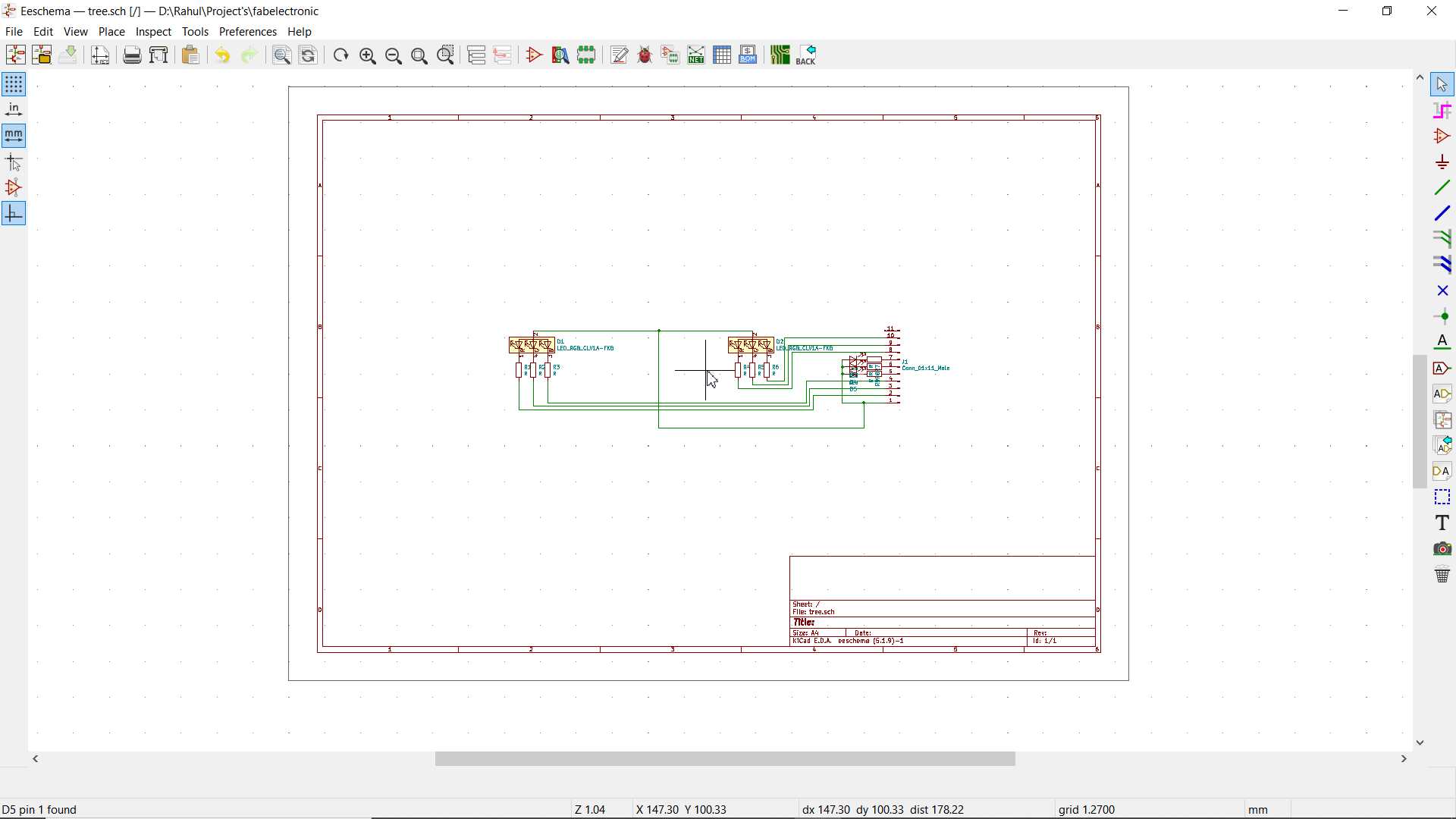
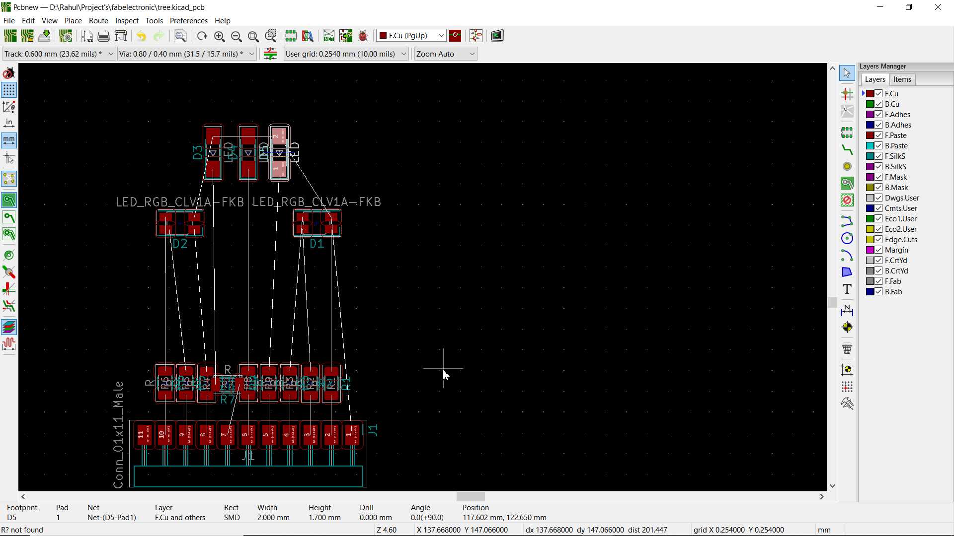
Here it took shape. Now my designing speed got increase here mean this took a hour to design whole thing
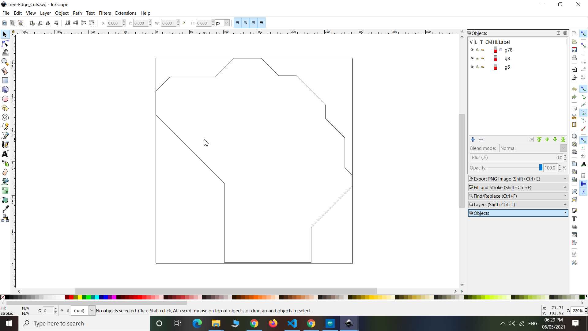
As you see in second pic here I used more kind of available layer in my design like those yellow filled part. I want it to be separate because this will get cut before cutting board outer edges
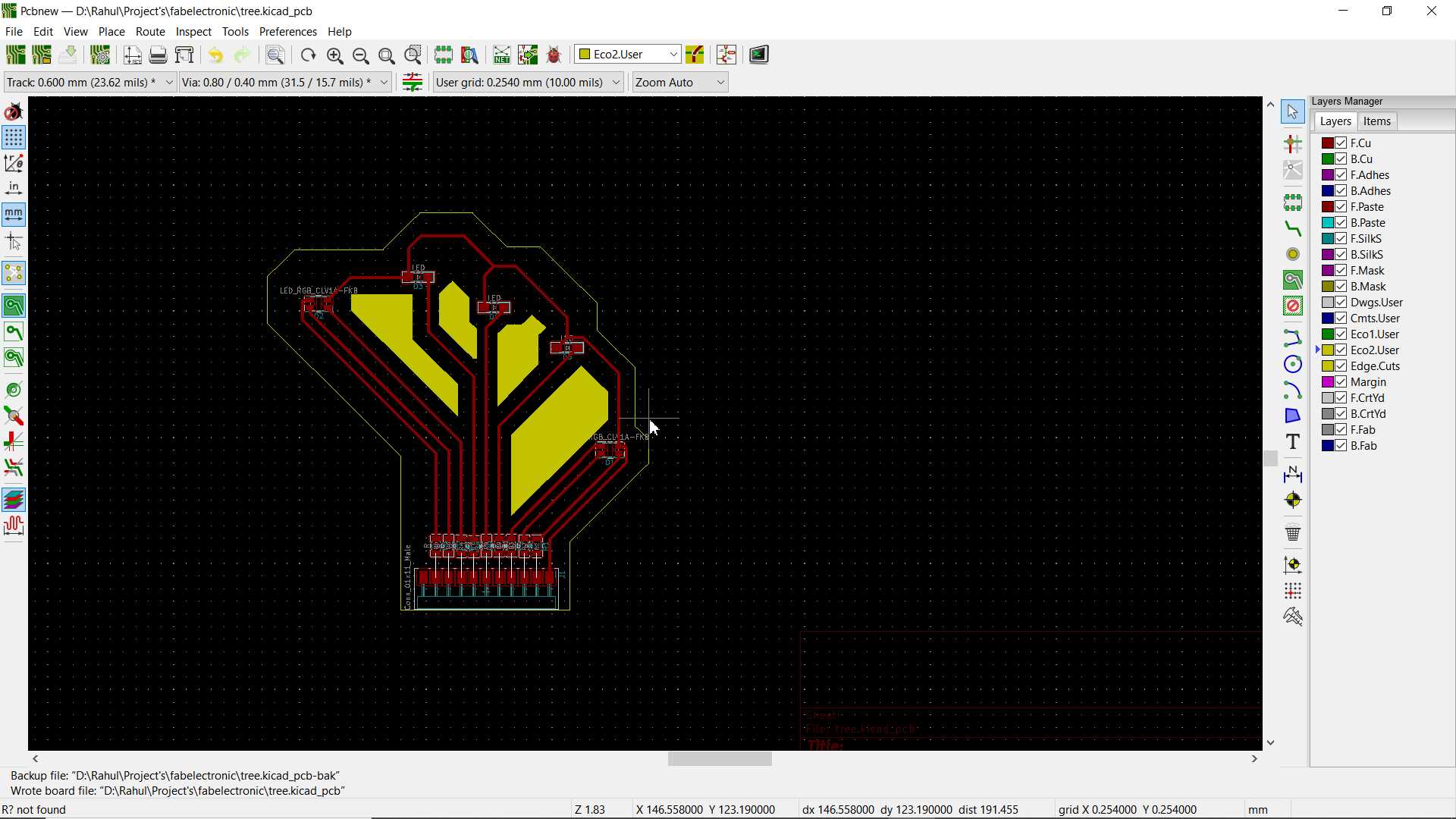
once design got completed I exported all layers in SVGs for mods
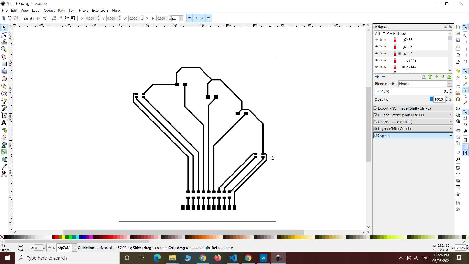
Used mods for Path generating and Milling with SRM20. As in all pcb milling I have used 1/64 end mill for Tracing and 1/32 end mill for cutting.
Before and After soldering and test
List of Components
- 1 x Blue Led
- 1 x Yellow Led
- 1 x Red led
- 2 x RGB LED common anode
- 9 x 499 ohms resistor (220 ohms is recommended)
- 1 x Female header 1x11 pins
.jpg)
.jpg)
So here I tested connection and leds and Made small program to run this design
int x=100;

void setup() {

  pinMode(9, OUTPUT);
  pinMode(5, OUTPUT);
  pinMode(4, OUTPUT);
  pinMode(3, OUTPUT);
  pinMode(7, OUTPUT);
  pinMode(1, OUTPUT);
  pinMode(0, OUTPUT);
  pinMode(2, OUTPUT);
  pinMode(6, OUTPUT);
  pinMode(10, OUTPUT);
  pinMode(8,INPUT_PULLUP);
}

void loop() {
  int y = digitalRead(8);
  if(y==0)
  {
    x=10;
     digitalWrite(9, HIGH);
  }
  else
  {
    x=100;
    digitalWrite(9, LOW);
  }
  digitalWrite(5, LOW);
  delay(x);
  digitalWrite(5, HIGH);
  delay(x);
  digitalWrite(4, LOW);
  delay(x);
  digitalWrite(4, HIGH);
  delay(x);
  digitalWrite(3, LOW);
  delay(x);
  digitalWrite(3, HIGH);
  delay(x);
  digitalWrite(7, LOW);
  delay(x);
  digitalWrite(7, HIGH);
  delay(x);
  digitalWrite(1, LOW);
  delay(x);
  digitalWrite(1, HIGH);
  delay(x);
  digitalWrite(6, LOW);
  delay(x);
  digitalWrite(6, HIGH);
  delay(x);
  digitalWrite(10, LOW);
  delay(x);
  digitalWrite(10, HIGH);
  delay(x);
  digitalWrite(0, LOW);
  delay(x);
  digitalWrite(0, HIGH);
  delay(x);
  digitalWrite(2, LOW);
  delay(x);
  digitalWrite(2, HIGH);
  delay(x);
}
Here How it is look like
After careful observation I came to know it is less look like tree and more look like Brain. So last I got another Idea and I Cut acrylic sheet in human head shap and stick my pcb's on it with glue. and finally It started to look like this.
Oh yeah!
Learning Outcomes:
So this week I done something creative and I am happy with it. I made tree shape pcb but after having different perception it turn into something I like even more. I got idea to use it on my laptop as cpu process indicator. I will explore this idea in my upcoming assignment of embedded programming.