

Electronics Production:
Objective:
1. Group assignment:
This week is having the following Objectives for the Group-
- Characterize the design rules for your PCB production process: document feeds, speeds, plunge rate, depth of cut (traces and outline) and tooling.
- document your work (in a group or individually)
2. Individual assignment:
Make an in-circuit programmer by milling and stuffing the PCB, test it, then optionally try other PCB fabrication process.
Learning Outcomes:
Described the process of milling, stuffing, de-bugging and programming
Demonstrate correct workflows and identify areas for improvement if required
Checklist:
Linked to the group assignment page ✔
Documented how you made (mill, stuff, solder) the board ✔
Documented that your board is functional ✔
Explained any problems and how you fixed them ✔
Included a ‘hero shot’ of your board ✔
Opening Quotes:
Electronics is clearly the winner of the day.--- John Ford
When I was a teenager in the late 30's and early 40's, electronics wasn't a word. You were interested in radio if you were interested in electronics. --- Ken Olsen
My hardcover sales are 17% down in books but up 400% in electronics. --- Lisa See
By the end of this decade, computers will disappear as distinct physical objects, with displays built in our eyeglasses, and electronics woven in our clothing, providing full-immersion visual virtual reality.--- Ray Kurzweil
Each of us is now electronically connected to the globe, and yet we feel utterly alone.---Dan Brown
Electronics Production:
The task of this week included assignments to be done in group and individually. We have to mill PCB plates, solder the components over it. For two weeks, we have been only working on the laptops. From last week, we have been making our hands dirty on the machines and learning to fabricate with the CNC machines.
Two of us already had experience of Milling and Soldering. They took lead and we divided the tasks amonst us. I have drafted the Group Assignment by taking the Snapshots, Screenshots and documenting the process. The details of the Group assignment could be found here.
Individual Assignment:
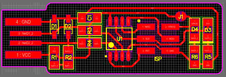
In this week, we had to individually mill, stuff, program the Fab ISP PCB plate.
A. PCB Milling:
PCB milling is the process of removing areas of copper from a sheet of printed circuit board material to recreate the pads, signal traces and structures according to patterns from a digital circuit board plan known as a layout file.
PCB milling is typically a non-chemical process and as such it can be completed in a typical office or lab environment without exposure to hazardous chemicals. High quality circuit boards can be produced using either process. In the case of PCB milling, the quality of a circuit board is chiefly determined by the system's true, or weighted, milling accuracy and control as well as the condition (sharpness, temper) of the milling bits and their respective feed/rotational speeds.(wikipedia)
A. Introduction to PCB Milling machine at FabLab-0 – Vigyan Ashram, Pabal:
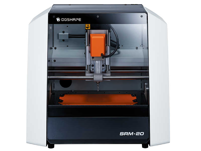
(Source: https://www.dgshape.com/en/srm-20/)
Introduction to Machine
After the Global review, next day we were introduced to the milling machine.
We have SRM-20 Milling Machine by DG Shape (Roland) in our FabLab. On Thursday, the 18th Fab. 2021 we were introduced to this machine by our Local Instructor (Mr. Suhas Labade). During the introduction, we were told about the DO's and DON'T's of the machine operation which included the Cleanliness of the machine and work area, ensuring safe and proper electrical connections. Door of the machine should be always closed while operating and giving commands or else it will not operate due to magnetic switch in the door for enhanced safety feature.
B. Preparing the SRM-20 machine for Milling:
Very first thing to start with the machine is to clean it and ensure proper electrical connections.
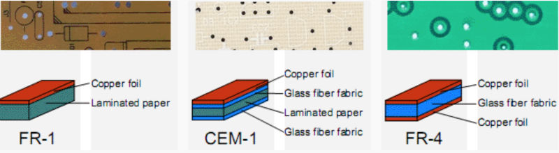
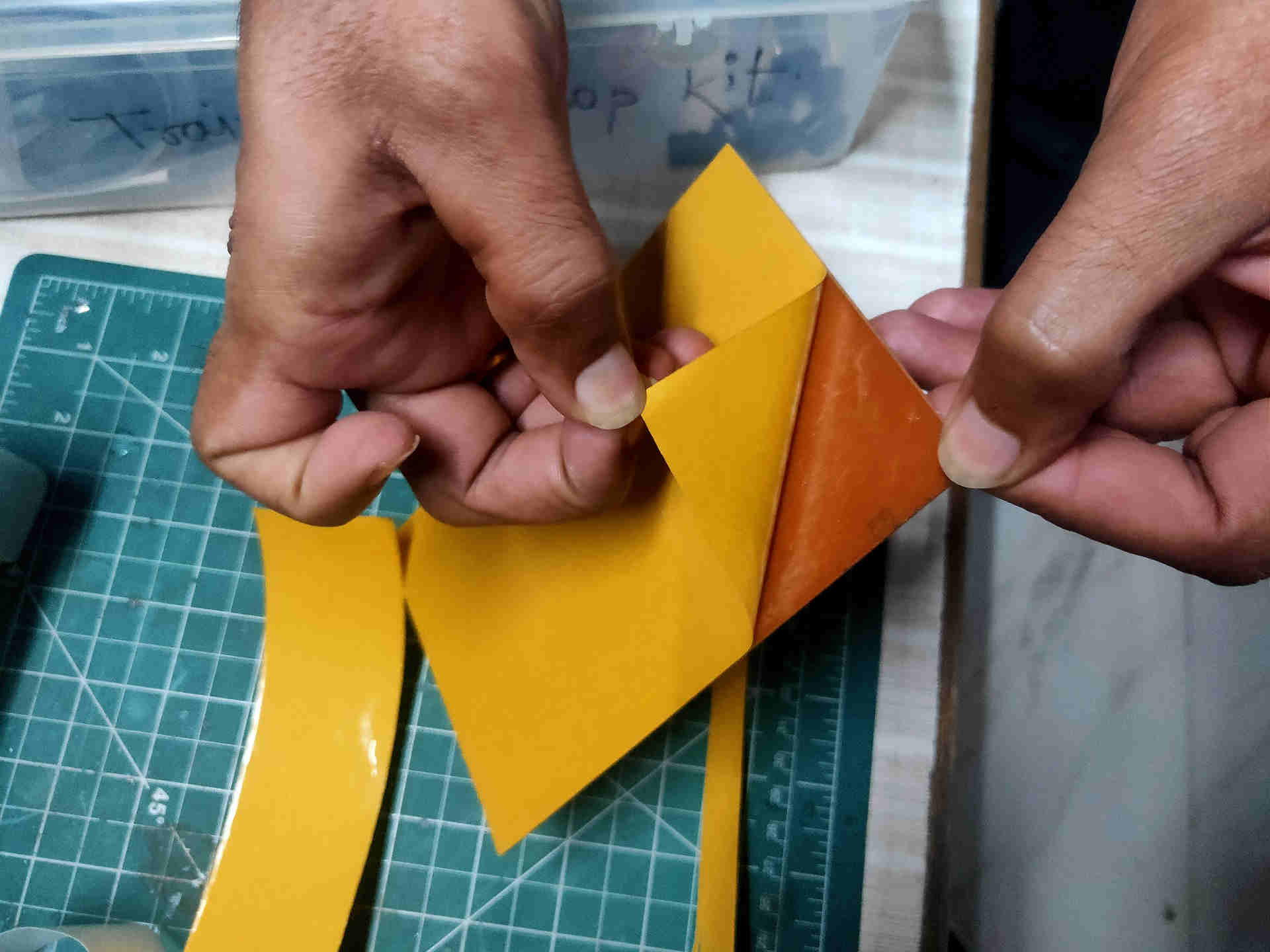
We have used the FR-1 material for PCB milling.
Our SRM-20 milling machine has used two layers of 12 mm acrylic sheets as sacrificial layers. This is because the head of the machine cannot reach the depth of the bed.
Steps followed by us for the operation of the Milling machine are as follows:
- 1. Unmounting the previously mounted PCB plate if any by using a Spatula.
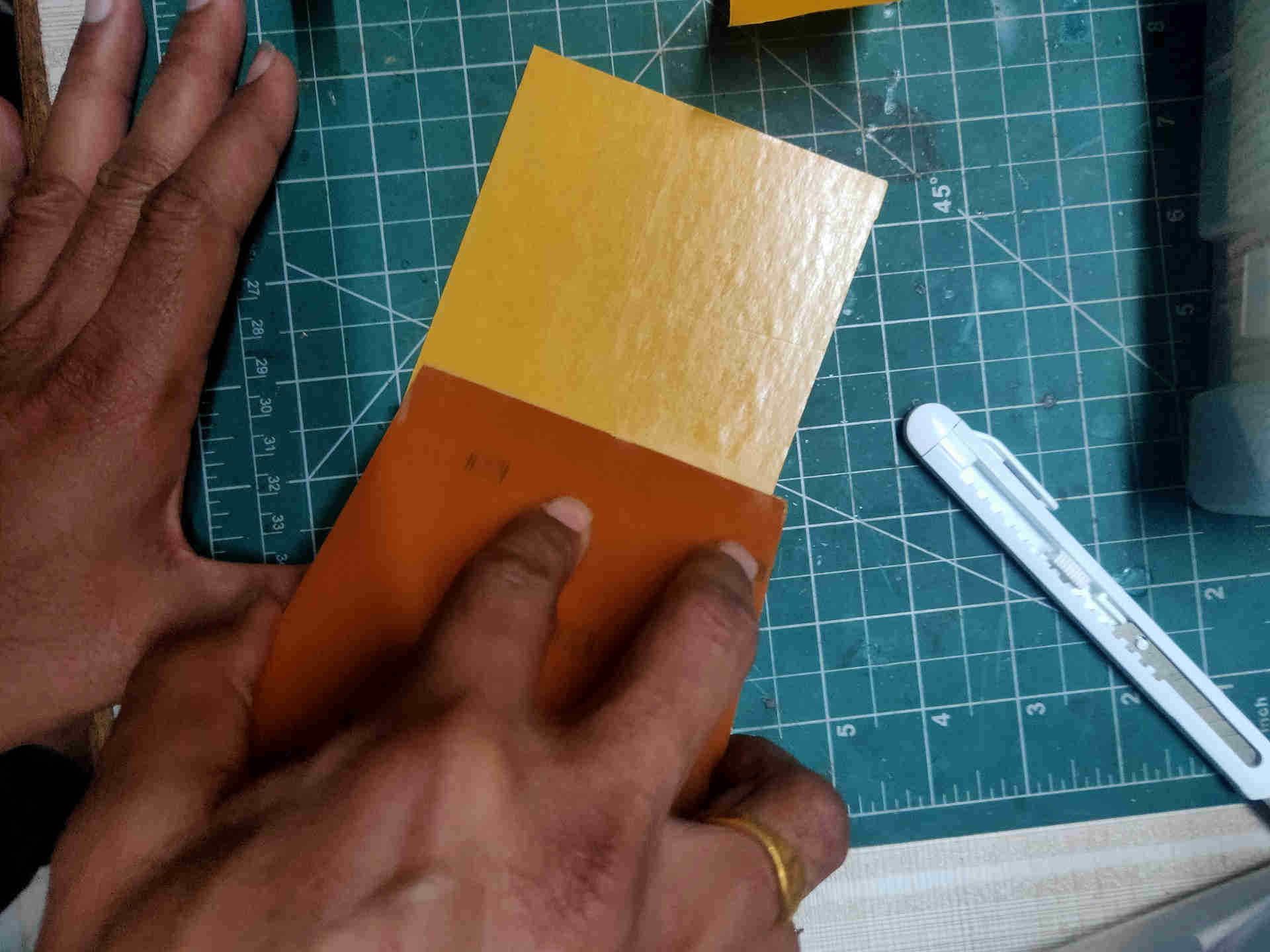
- 2. Cleaning the sacrificial layer by acetone
- 3. Ensure complete removal of the adhesive tape from the bed.
- 4. Use Vacuum cleaner to clean any residues.
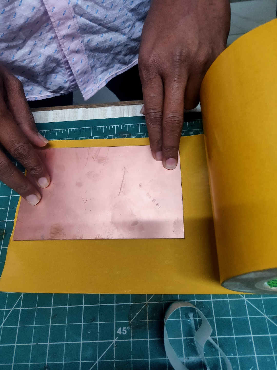
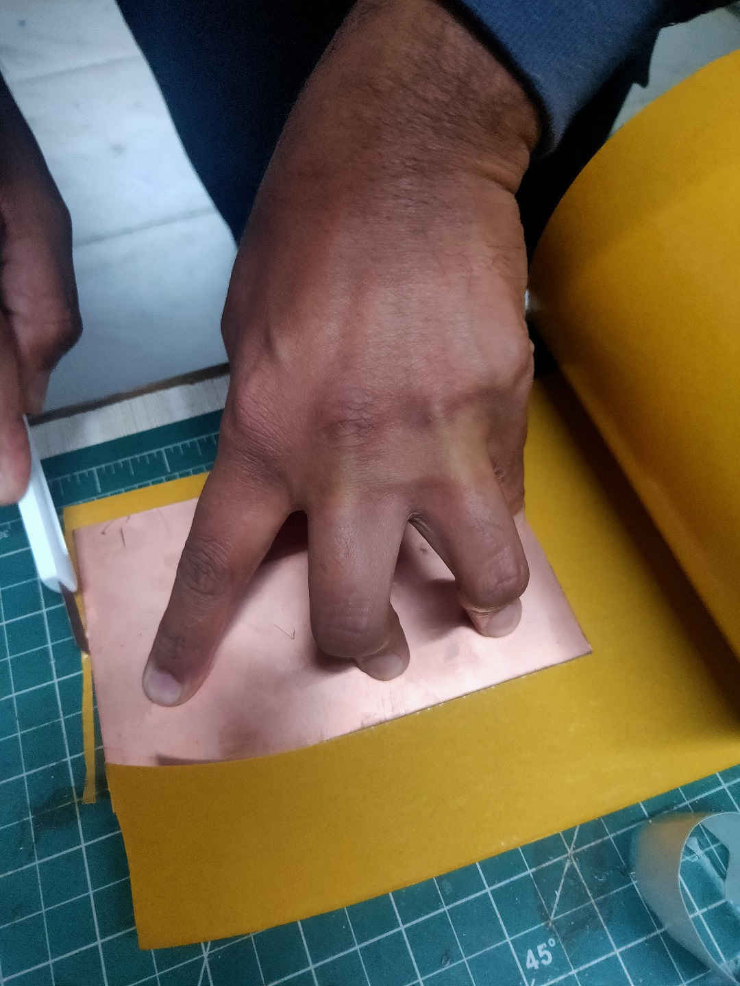
- 5. Select and use an already cut piece of the PCB plate (FR-1) Size: about 4 x 6 in.
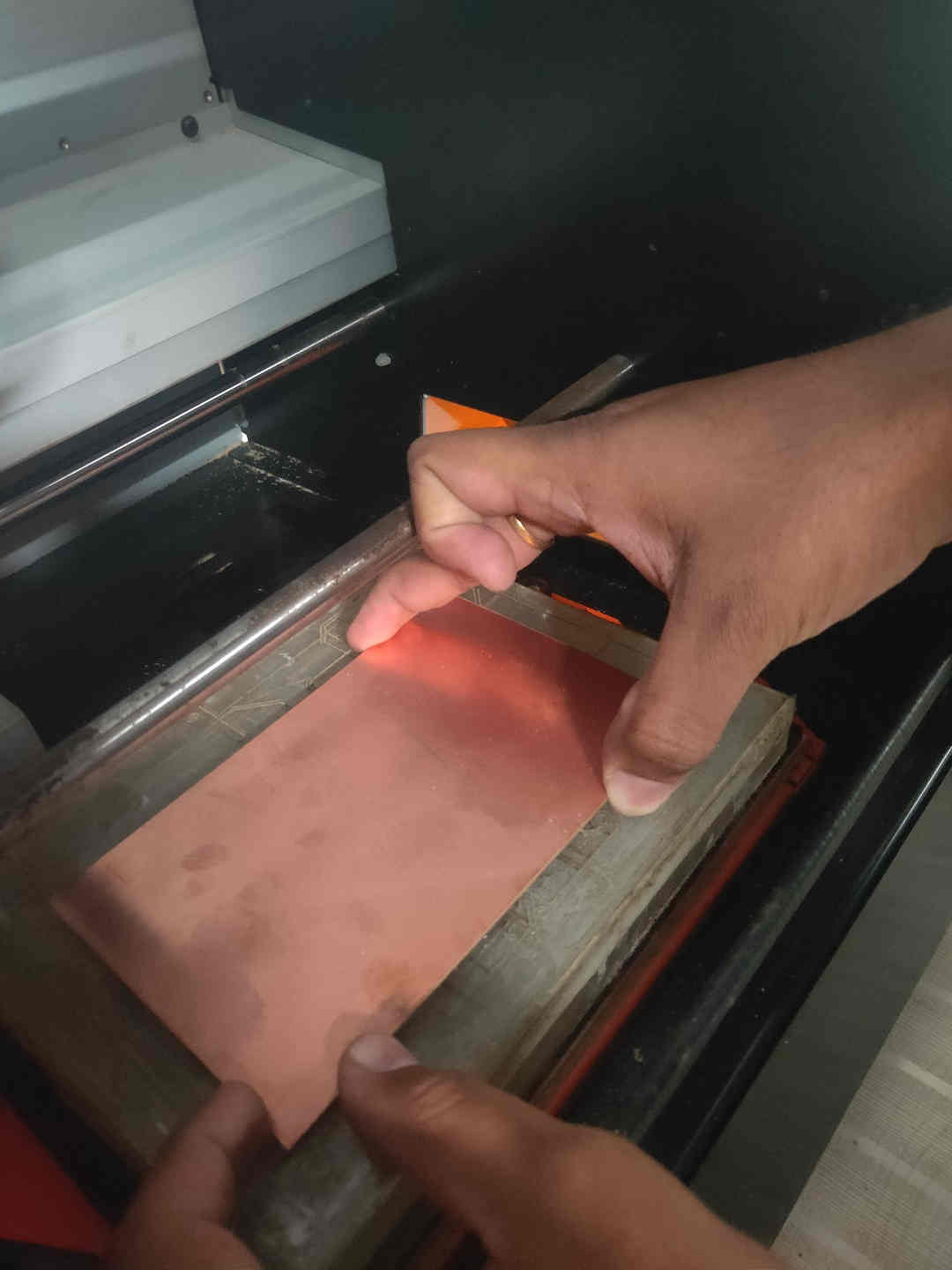
- 6. Clean the PCB plate and remove any dust or sticky material over it
- 7. Ensure that the plate is completely horizontal.
- 8. Remove the bubbles if any by sliding another plate over it.
- 9. Remove the cover of the adhesive tape.
- 10. Properly mount the PCB plate on the bed of the machine.
- 11. Press gently for proper adhesion (or else the PCB plate will pop up after the cut or may even have burring and improper trace cut.)
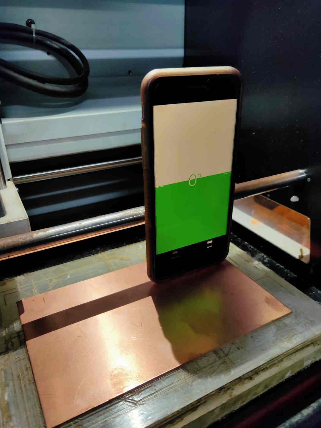
- 12. Use the levelling the gadget to ensure horizontal surface. We were working in the night so we have used function from iPhone 6S.
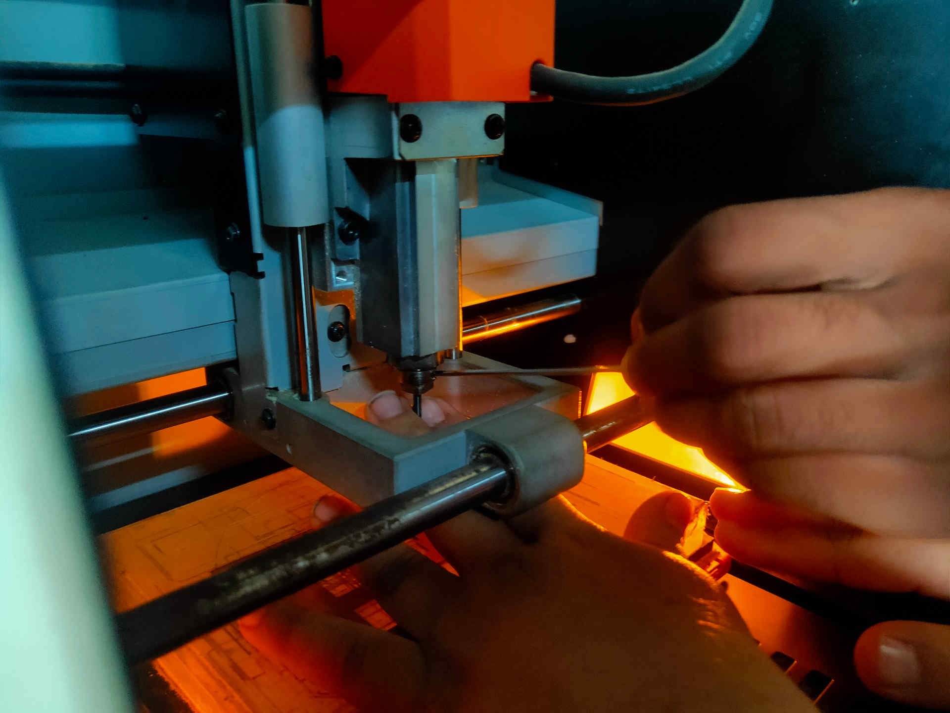
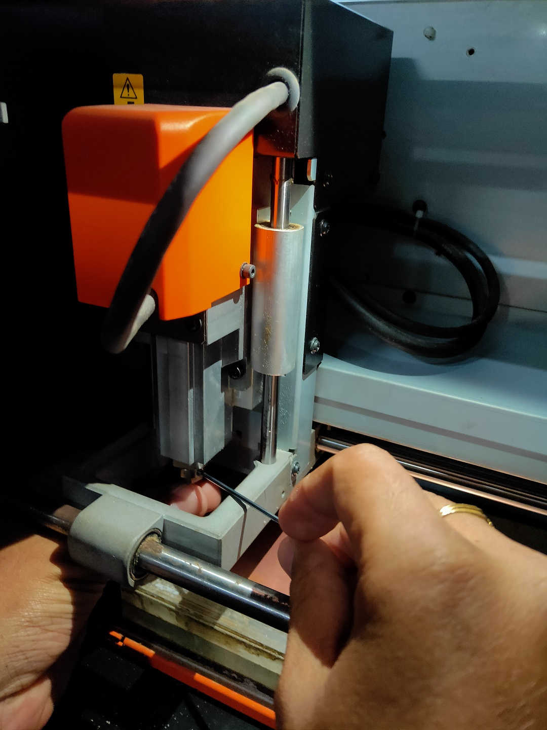
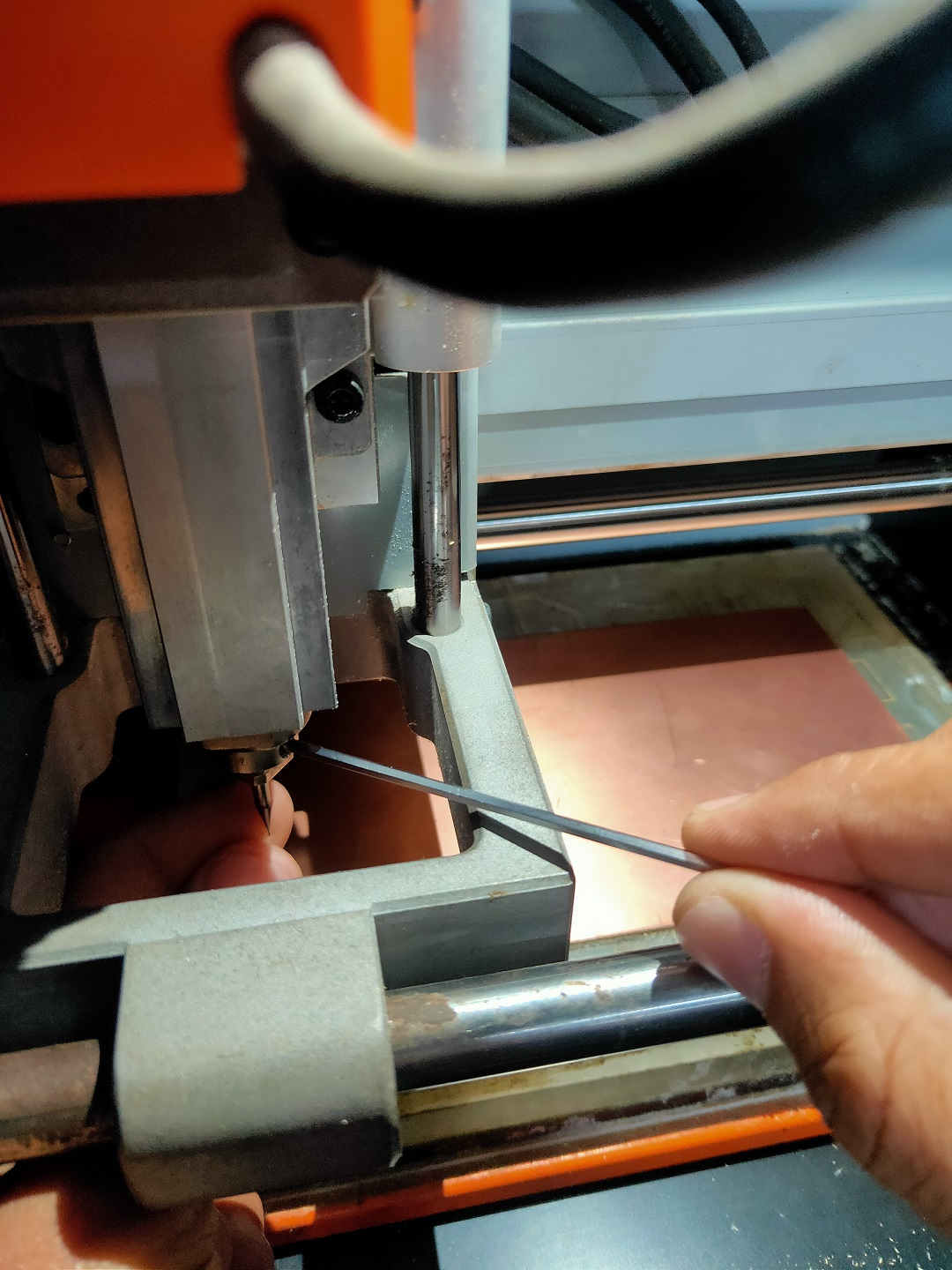
- 13. Once the plate is firmly set-in position, we then moved on to mount the drill bit.
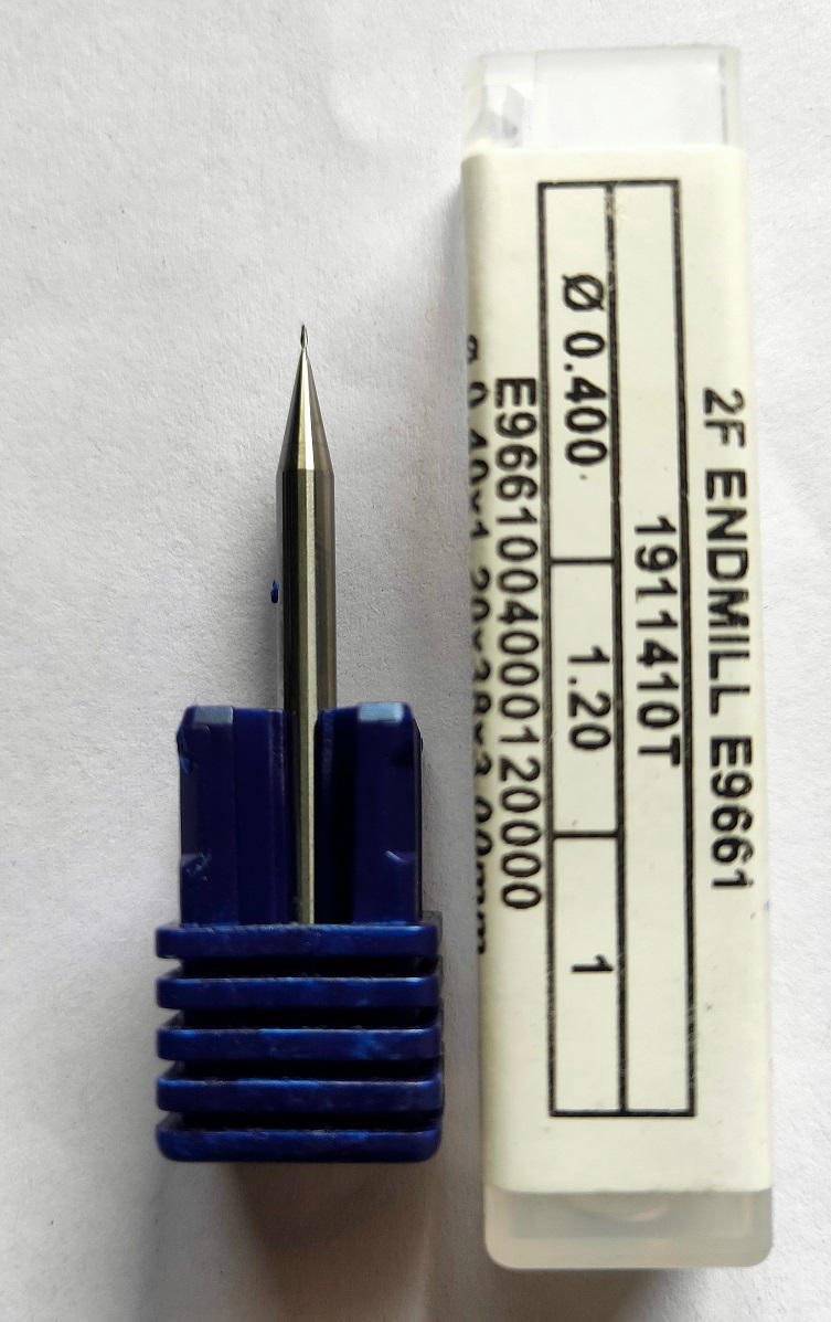
- 14. We have used the 1/64 drill bit for the trace cut of the PCB plate.
15. The process of setting / mounting the drill bit is as follows:
- i. Bring the header and the bed area in centre by giving command from the mods so that it is accessible.
- ii. Loosen the chuck using the allen key by turning it in the anticlock wise direction.
- iii. Insert the 1/64 drill bit in the chuck by one hand and tighten the chuck using allen key by other hand. *(There are two holes; one is where the allen key fits properly and simply rotates in the other hole.) *(Do not apply too much pressure on the allen key; it is programmed to automatically lock itself even if gently forced.)
- iv. Set the z- axis to a height of 7-10 mm above the bed.
- v. Loosen the chuck and let the drill bit to descend down by gravity.
- vi. Tighten the chuck by using allen key and turning it in the clockwise direction.
- vii. Note down the coordinates of the origin.
- viii. Close the door of the machine.
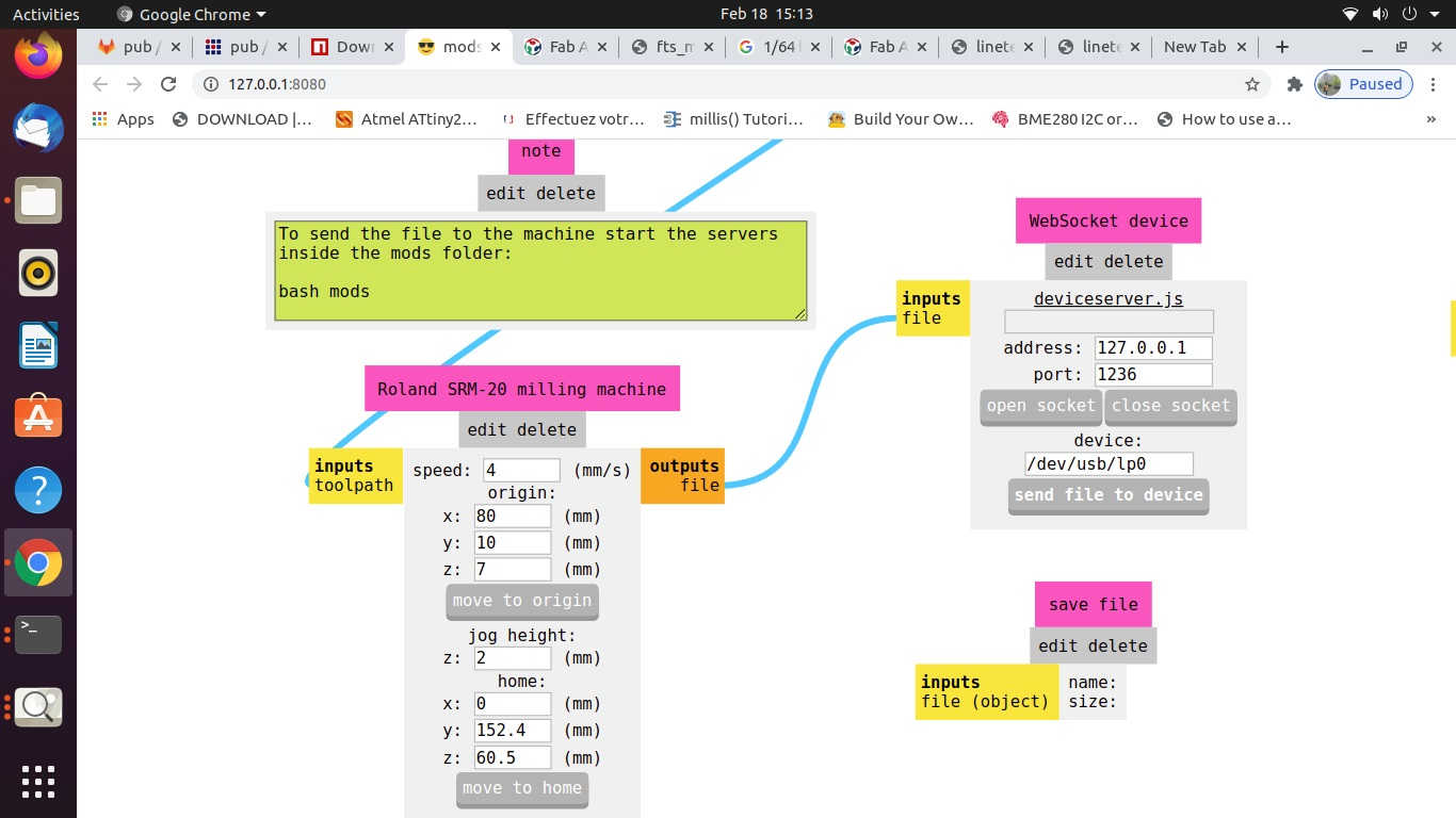
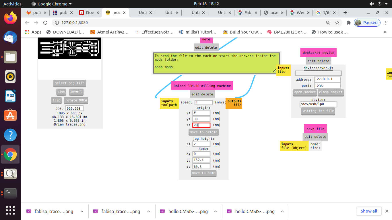
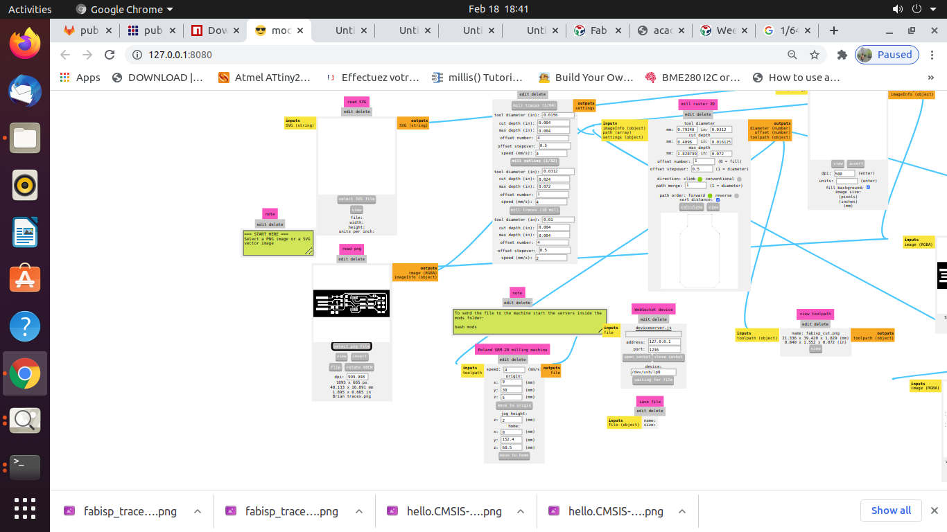
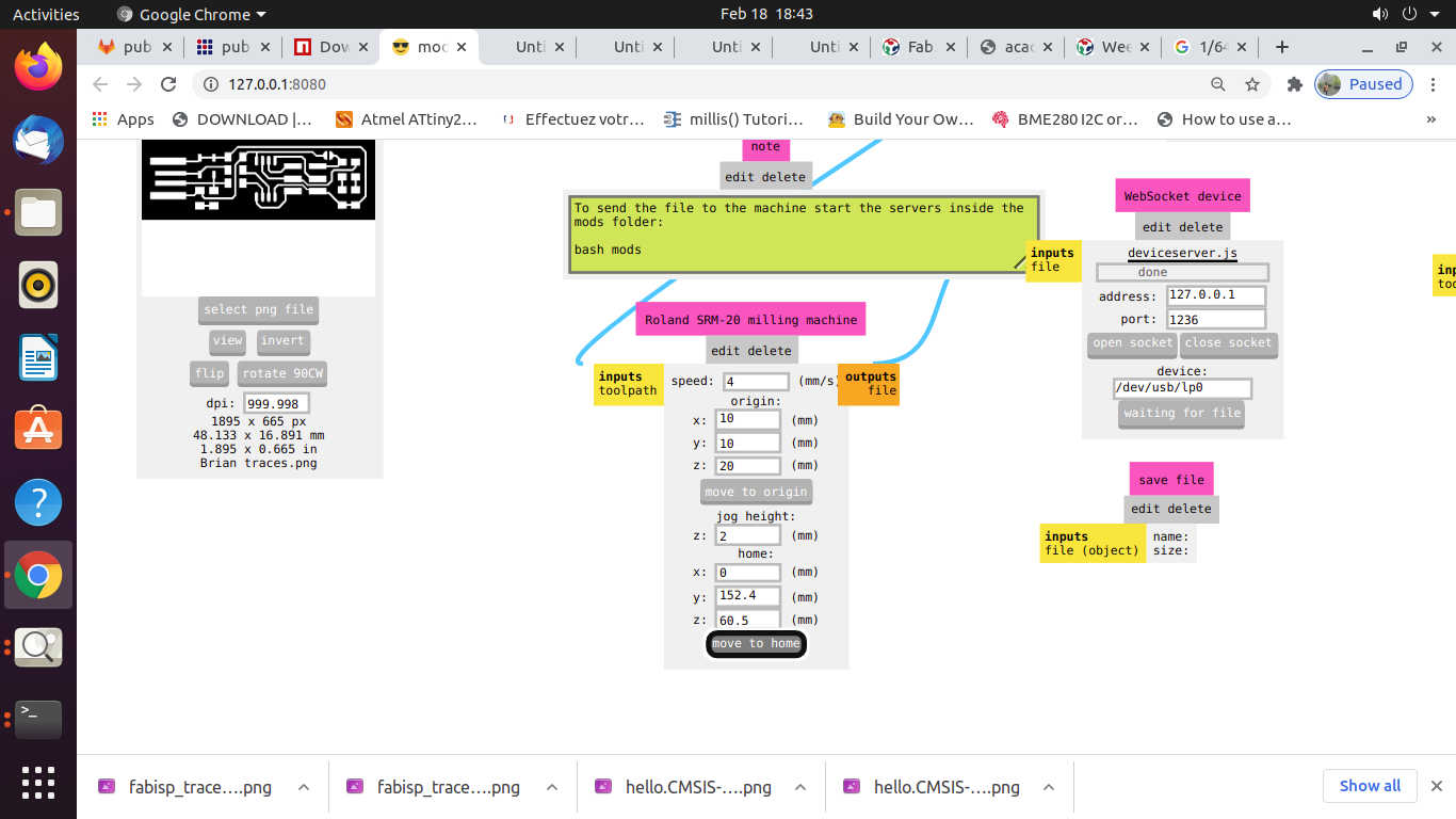
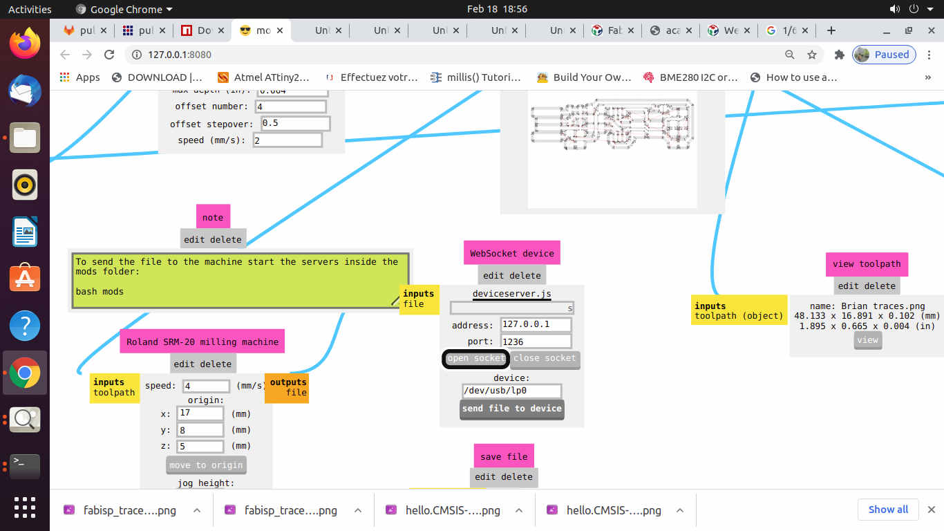
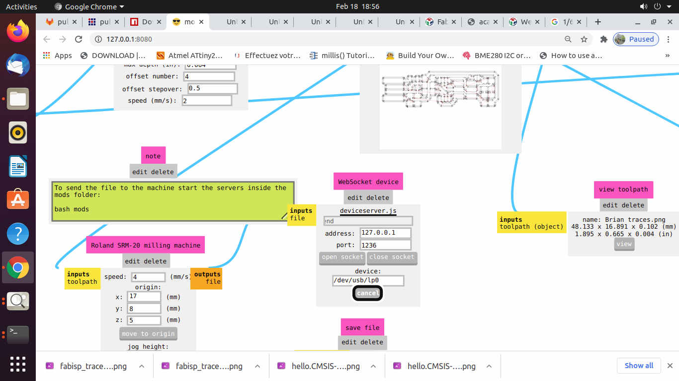
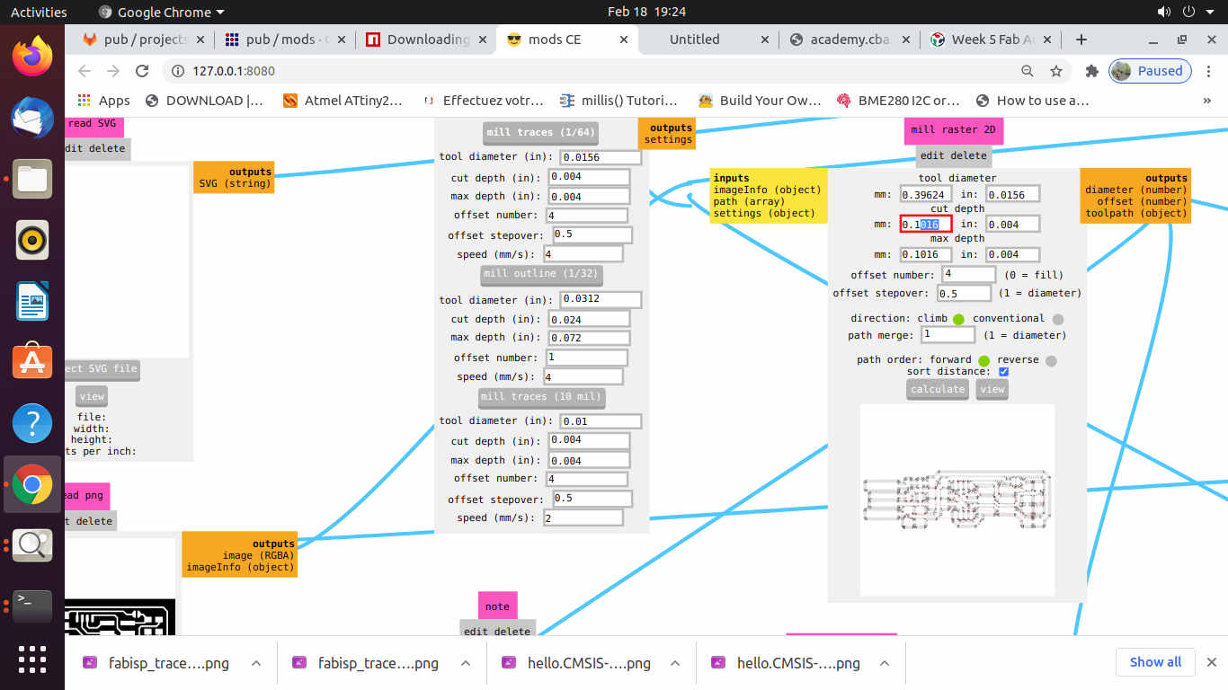
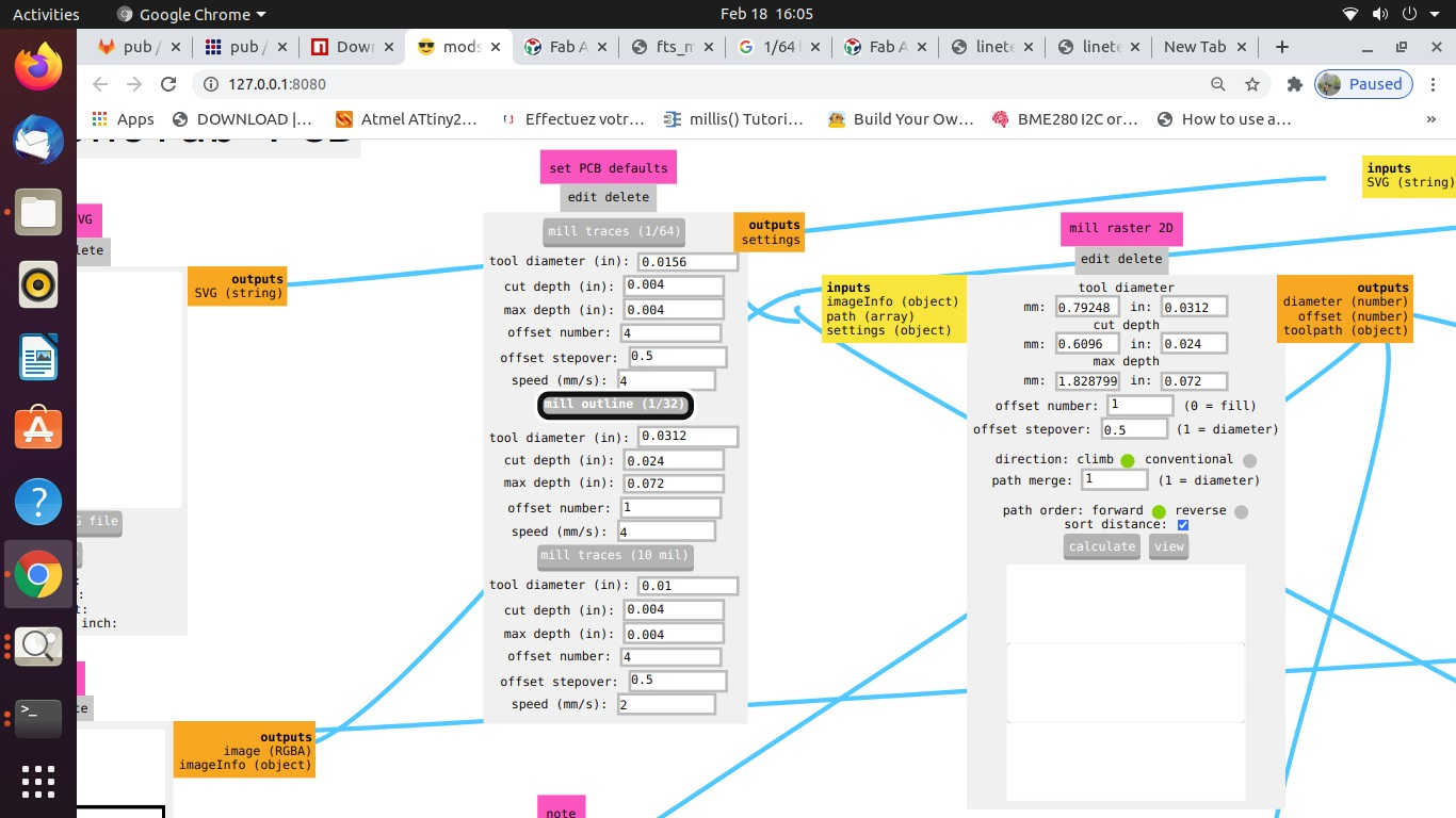
C. CAM Operation (Configuring / Generating Tool Path using MODS):
The process of CAM operation or Configuring / Generating Tool path is as follows:
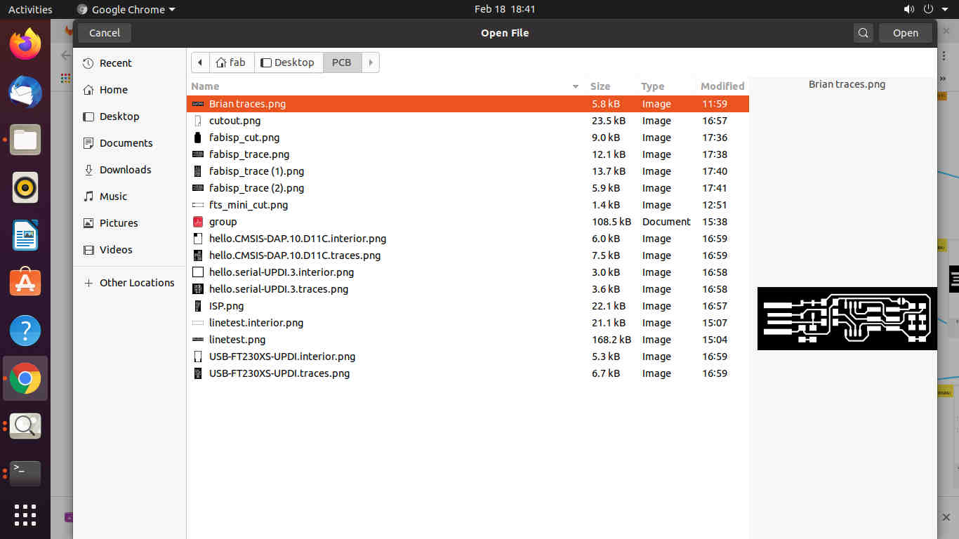
- i. Download the two images of FAB ISP Trace cut by Brian and Fab ISP interior from the fabacademy website.

- ii. The module was already installed in the desktop PC attached with the SRM-20 milling machine in our lab. You may learn, download and install it by following the process explained here. (link: https://gitlab.fabcloud.org/pub/project/mods)
- iii. The process of operating MODS is as:
- Boot the Desktop terminal using Ubuntu OS.
- Open Terminal and use commands --> cd Documents/mods
- cd Documents to change directory --> mods --> bash mods
- Again, Open New Terminal and use commands
- cd Documents --> http – server
- This will open a Window in Google Browser.
- Right Click in the Window
- Four options will be displayed like Modules, Programs, Edit, Options etc.
- Select Programs --> Select Open --> Select SRM-20 Mill -->
- Go through each step of the Module -->Select the Photo/Image to be used for milling
- Check the format of the image (.svg or .png)
- Check the selection of drill bit for Cut trace (1/64) or cut outline (1/32), Tool Path, Tool Diameter, Cut Depth, Offset, Stepovers, Speed and the position of the X, Y and Z axes.
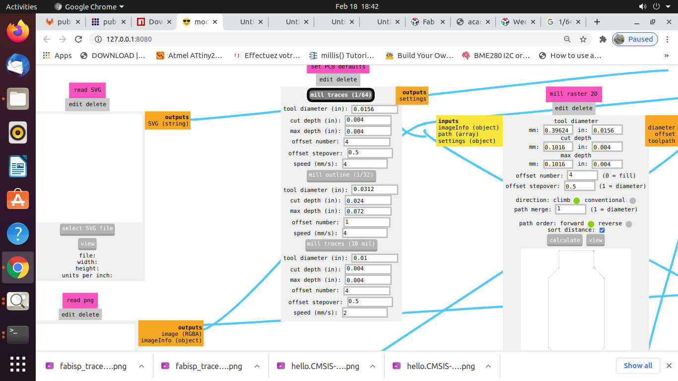
 *(Always pay attention to the position of Z axis while setting the origin or moving to the home and coming back to the origin position.
 - Open the Socket to enable communication between the computer and the machine
- Calculate the path
- Send the File for milling.

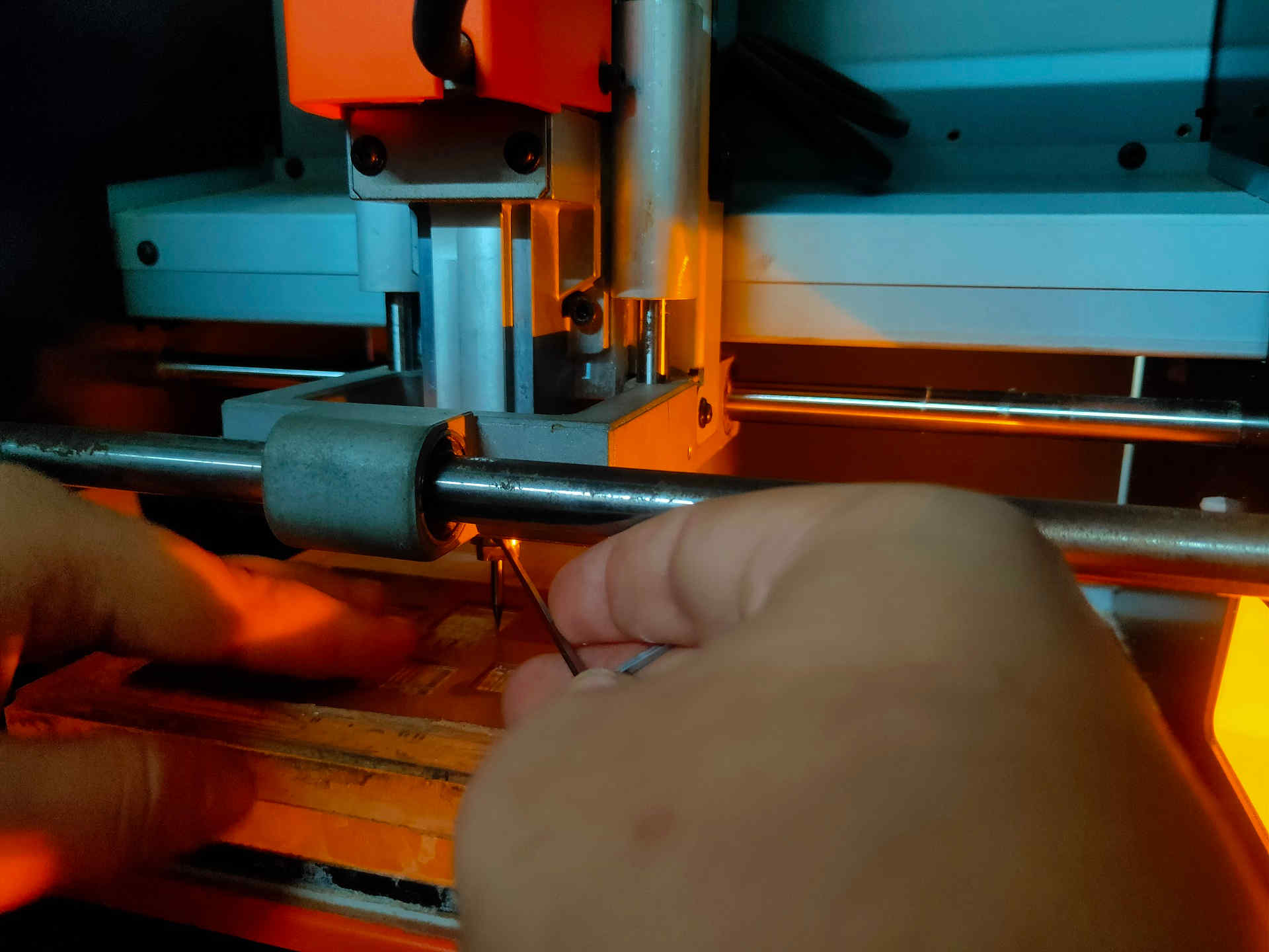
D. PCB Milling (Trace Cutting and Outline Cutting):
- i. Do not leave the machine unattended while the milling is going on.
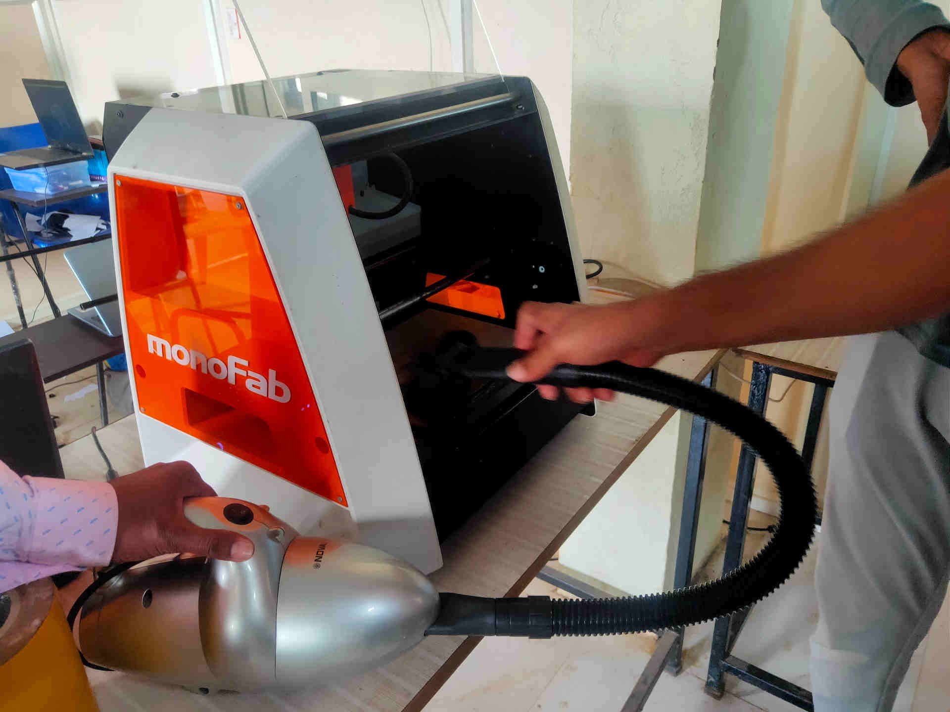
- ii. After the completion of the trace image on the PCB plate, open the door of the machine.
- iii. Use vacuum cleaner to clean the residual particles. DO NOT try to clean the particles by blowing air through the mouth as these particles are hazardous and may cause illness.
- iv. Check the plate for proper milling.
- v. If the plate is not properly milled, change (increase) the cut depth and give a double pass without changing the position of the plate and the drill.
- vi. Once, the plate is properly milled with cut trace, move the Z axis in upward direction, loosen the chuck using the allen key and moving it in anticlock wise direction.
- vii. Unmount the 1/64 drill bit used for cut tracing.
- viii. Take 1/32 drill bit and mount it to the Chuck.
- ix. Properly tighten the drill bit and set the origin.
- x. Again, check the tool path using MODS and select the mill outline drill bit; check the Tool Diameter, Cut Depth, Offset, Stepovers, Speed and the position of the X, Y and Z axes.
- *(Always pay attention to the position of Z axis while setting the origin or moving to the home and coming back to the origin position.
- xi. Open the Socket to enable communication between the computer and the machine
- xii. Calculate the path
- xiii. Send the File for milling.
- xiv. After the milling of the cut outline is completed, use vacuum cleaner to clean the debris.
- xv. Collect the PCB plate.
- xvi. Clean the adhesive tape adhered to the base of the plate.
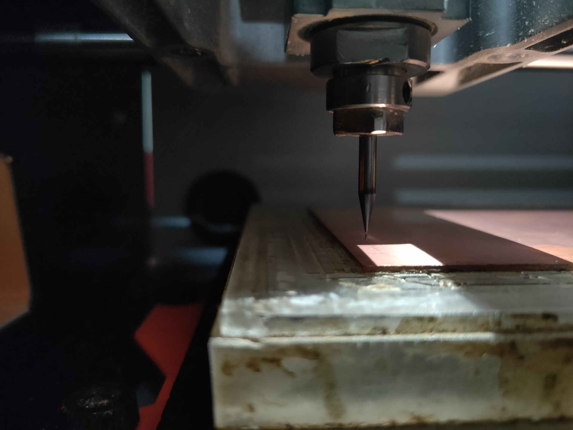
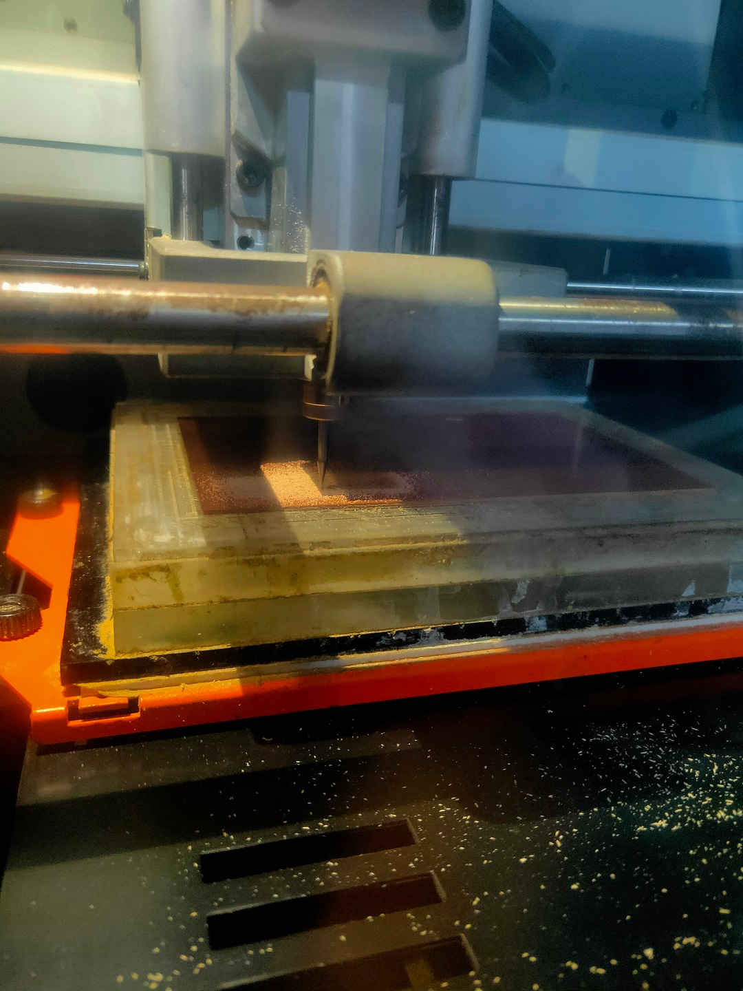
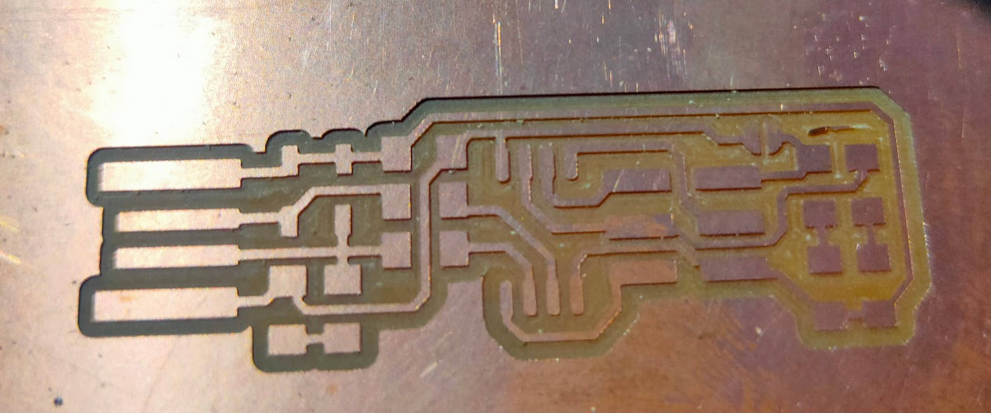
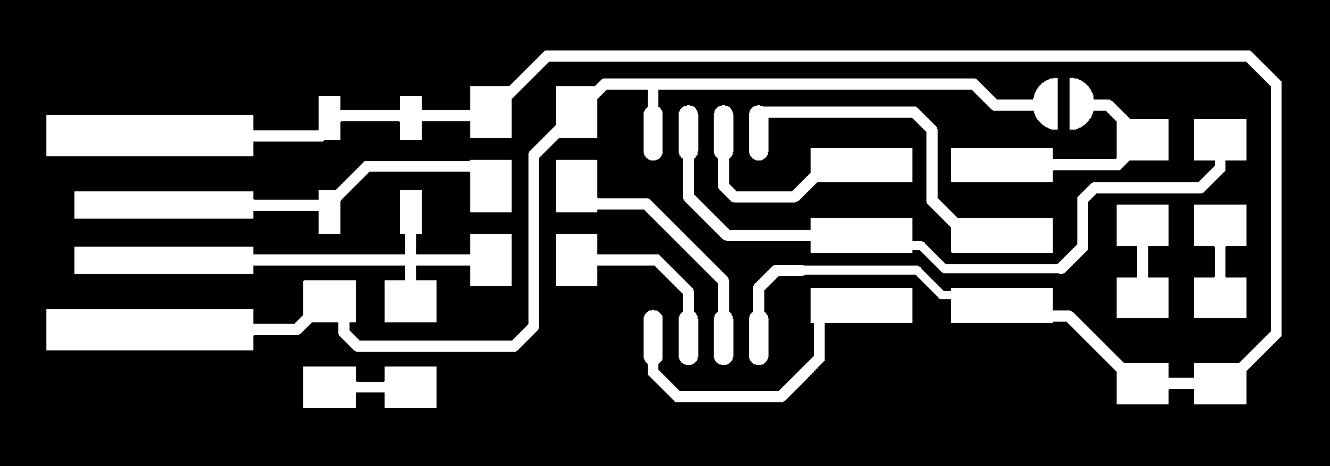
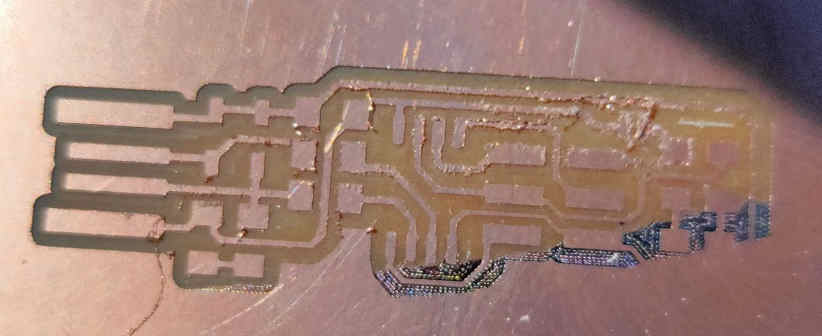
The PCB plate after milling cut trace.
Cut Outline milling ongoing
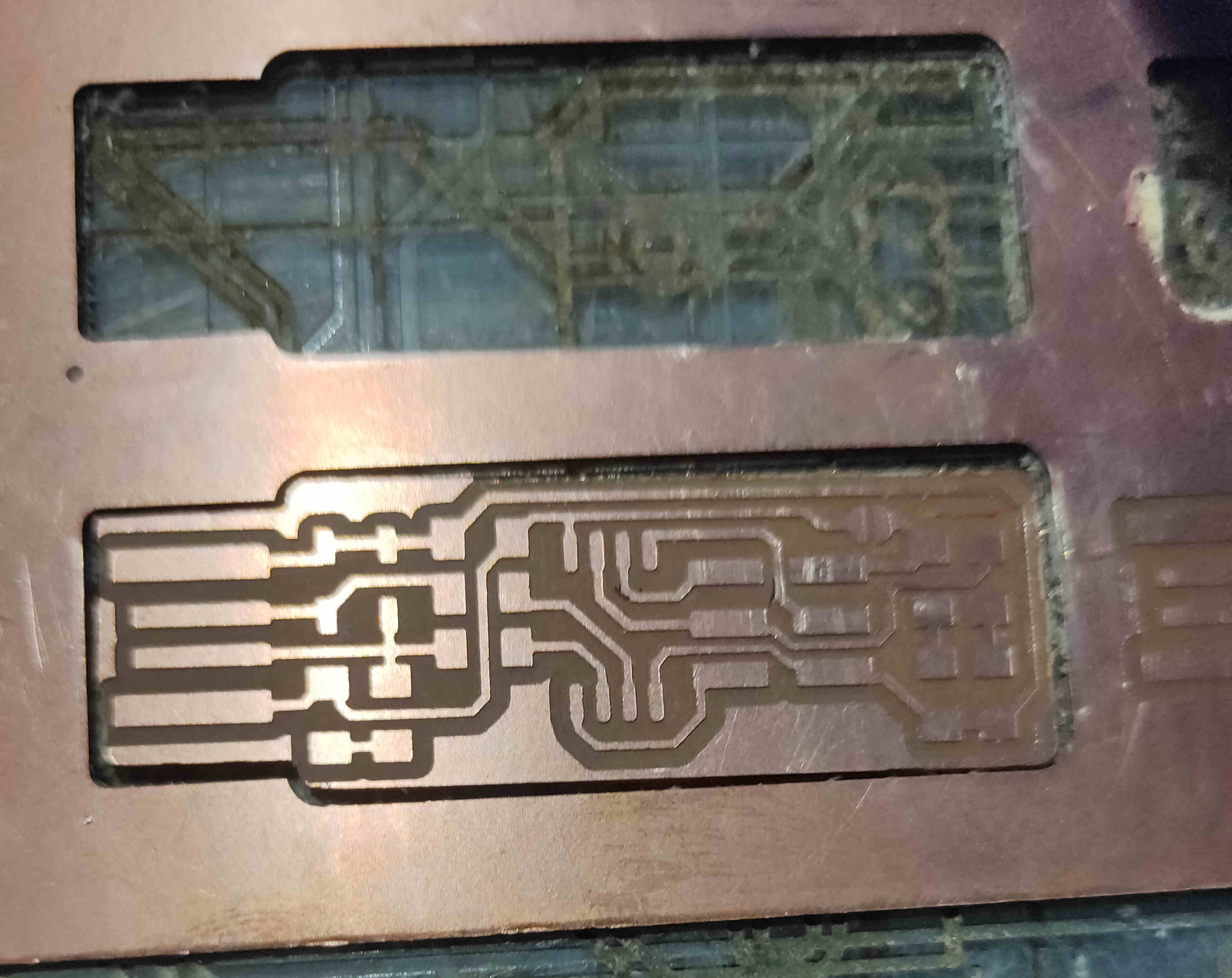
I tried to mill another PCB but due to uneven surfac and improper levelling of the overlay and bed area, it had burring and superficial trace cut. I didnt tried double pass as it already had the burring.
E. Learnings:
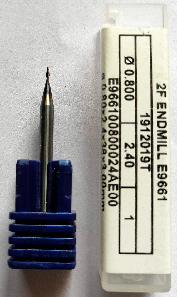
- i. Feeds:
- Tool Diameter for cut traces- 1/64 drill bit – 0.0156 mm
- Tool Diameter for cut outline- 1/32 drill bit – 0.0312 mm
- Image Size: 48.133 x 16.891 mm (1895 x 665 px)
- ii. Speed: 4 mm/sec.
- iii. Depth of Cut: for Trace cut – 0.004 in.
- Outline cut – 0.6096 in (minimum)
- 1.8287 in (maximum)
- iv. Tooling:
- FR-1 PCB plates for milling
- L-N key for mounting and unmounting drill bits to chuck of the machine.
- Drill bit of 1/64 for Fab ISP mill trace cut
- Drill bit of 1/32 for Fab ISP mill outline cut
- Spatula for unmounting the PCB plate off the Overlay / sacrificial layer.
- Vacuum cleaner for cleaning
- Level Tube for checking the level of the bed area
F. Caution:
- 1. Ensure Cleanliness and proper electrical connections of the machine.
- 2. Do not blow the air by mouth to clean the residues of the milling. Use vacuum cleaner.
- 3. Always carefully handle the drill bits as they may break if mishandled.
- 4. Check (set higher than 10 mm) the position of the Z axis before moving to Home or Origin position.
- 5. Ensure the completely horizontal position of the plate after mounting on the bed.
B. PCB Soldering:
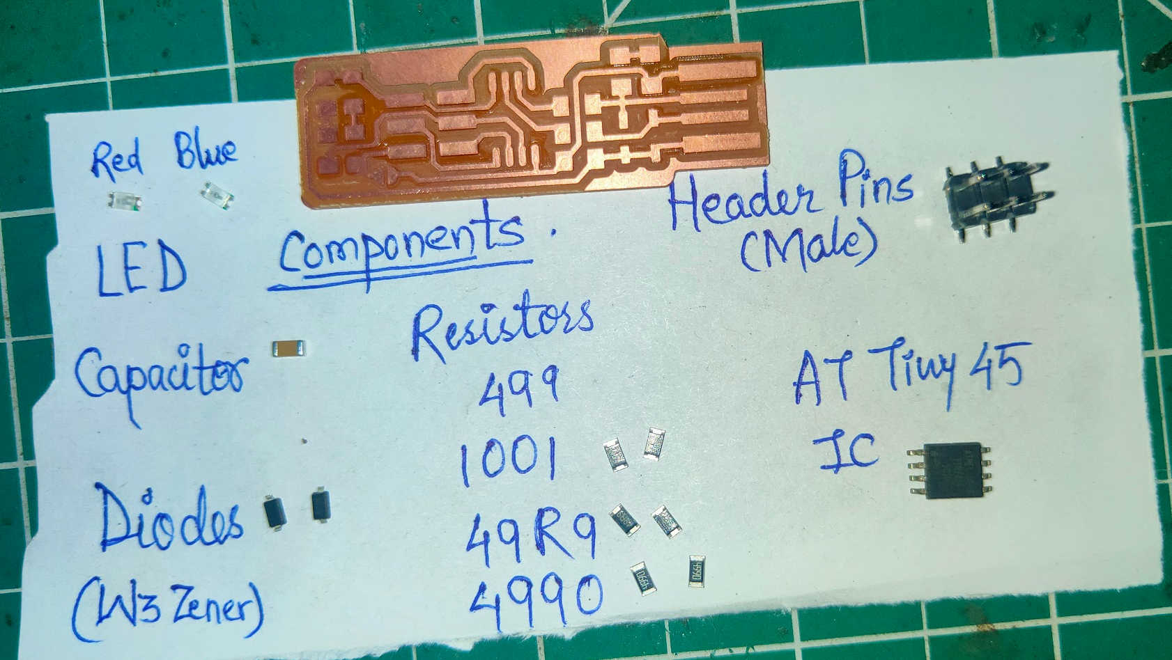
Soldering is an especially common requirement for jobs involving circuit building, PCB assembly and electronic prototyping. For this assignment, we will be soldering the following components of FAB ISP PCB plate as given in the Brian’s Fab Academy page
- Components required for the fabrication of Fab ISP by Brian are:
- 1x ATtiny45 or ATtiny85
- 2x 1kΩ resistors
- 2x 499Ω resistors
- 2x 49Ω resistors
- 2x 3.3v zener diodes
- 1x red LED
- 1x blue LED
- 1x 100nF capacitor
- 1x 2x3 pin header
Tools required for the fabrication of Fab ISP by Brian are:
Appropriate tools are always necessary to make a clean soldering. Also it will make our life easier.
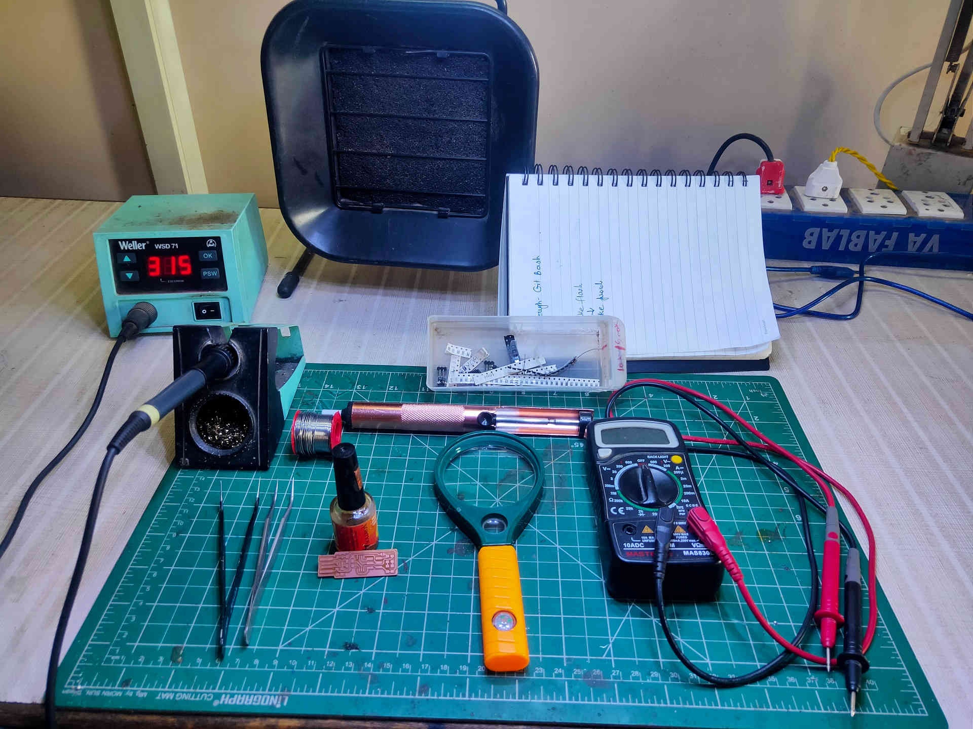
- Tweezer for holding and picking up the components
- Soldering Iron and Stand
- Solder Wire
- Flux
- Magnigying Glass
- Lamp
- Hot Air Gun
- Desoldering braids/Suction Pump
- Exhaust
- Cutting Mat
- Lots and Lots of Patience and Focus
Being new to the Electronics, I first tried to understand the components by asking about what is called what? how does it looks? what it does? how to differentiate?
The components used in the SMD PCB fabrication are altogether different than those used in the Throughhole PCB fabrication.
I also tried to understand about the polarity of the Diodes, LED's and the Integrated Circuits (IC's)
I came to know that :
This was first time of soldering in life. I first tried soldering on the old Through hole PCB plates by desoldering the attached components by using desoldering hot air gun. Then I soldered few components again.
Then, I desoldered the components on SMD PCB plates and soldered them again. My hands were shaking and water rolling out of eyes due to focus while soldering the tiny components.
After this net practice, I then collected all the required components and started soldering. I approached by first soldering the small components and then atlast soldering the IC and Connector pins. This will allow you sapce for working. If the connector pins and IC are soldered first, it will be difficult to solder the smaller components.
Some Issues that I faced were:
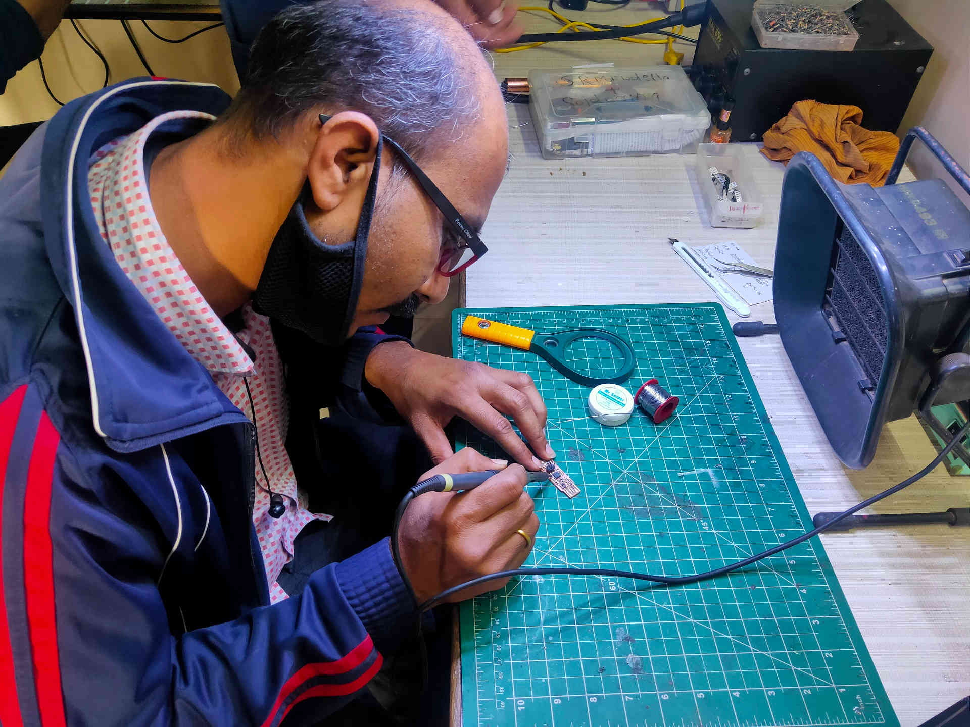
My approach to Soldering after observing my experienced colleague changed.
I, now-
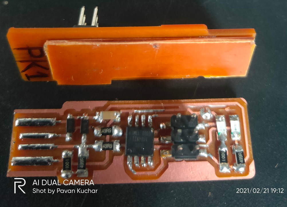
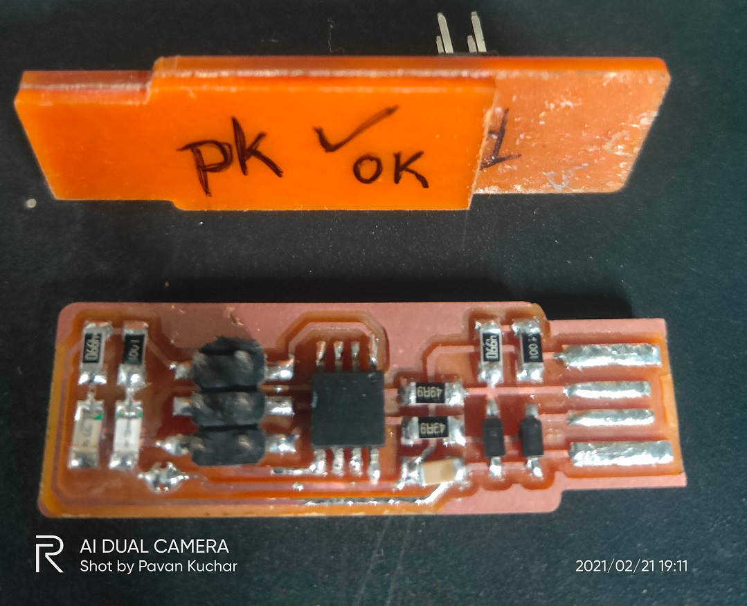
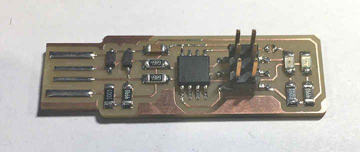
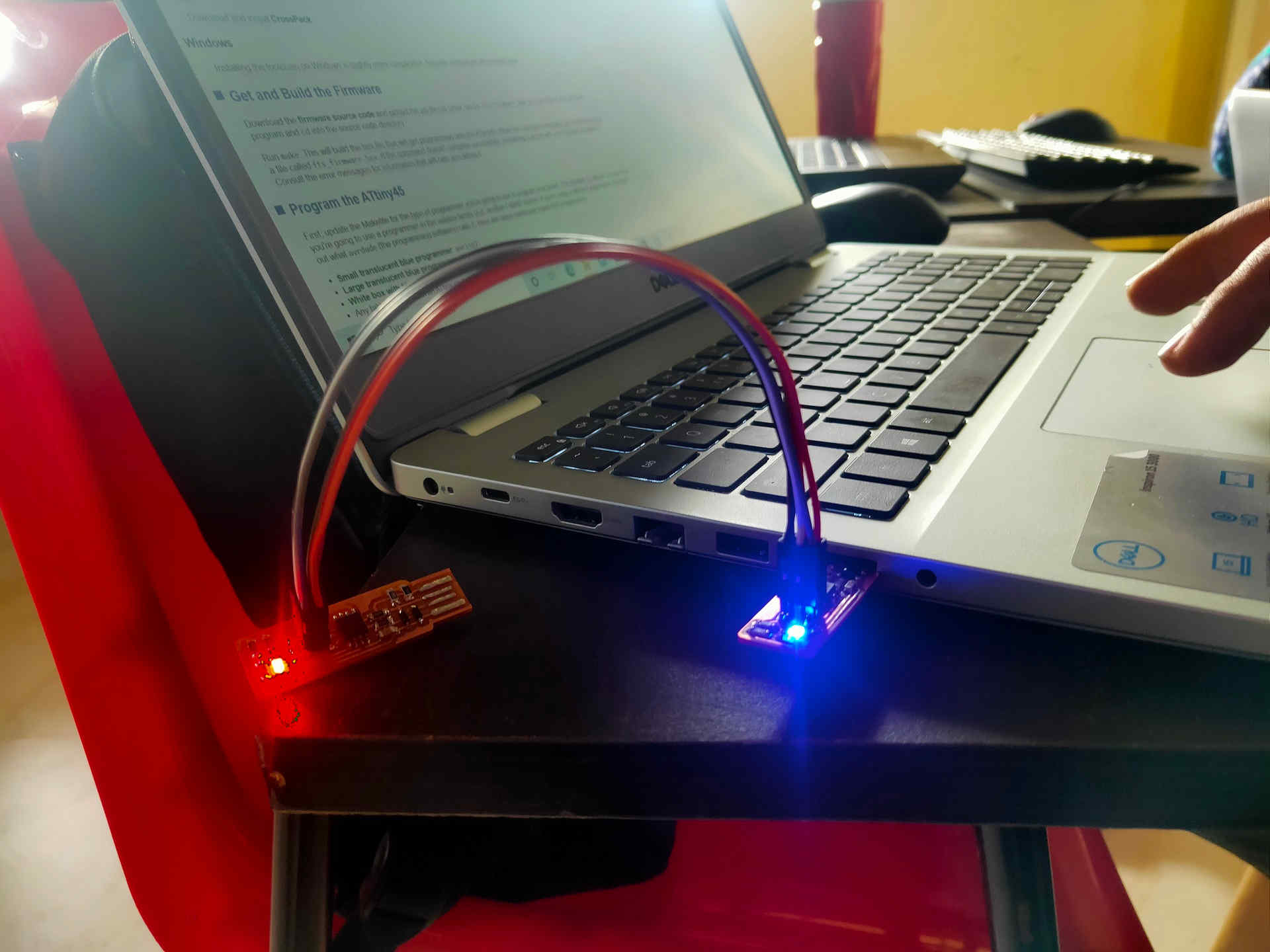
Hero Shots of my Board
PCB Programming:
I am having Windows OS on my Laptop. So, I had to install the required programs and softwares to Program the fabricated Fab ISP. It is easy to do on the Linux OS by command line.
The process for Using the GNU AVR toolchain can be found here.Building the Fab Tiny ISP
The process for Using the GNU AVR toolchain on Windows 10 can be found here.
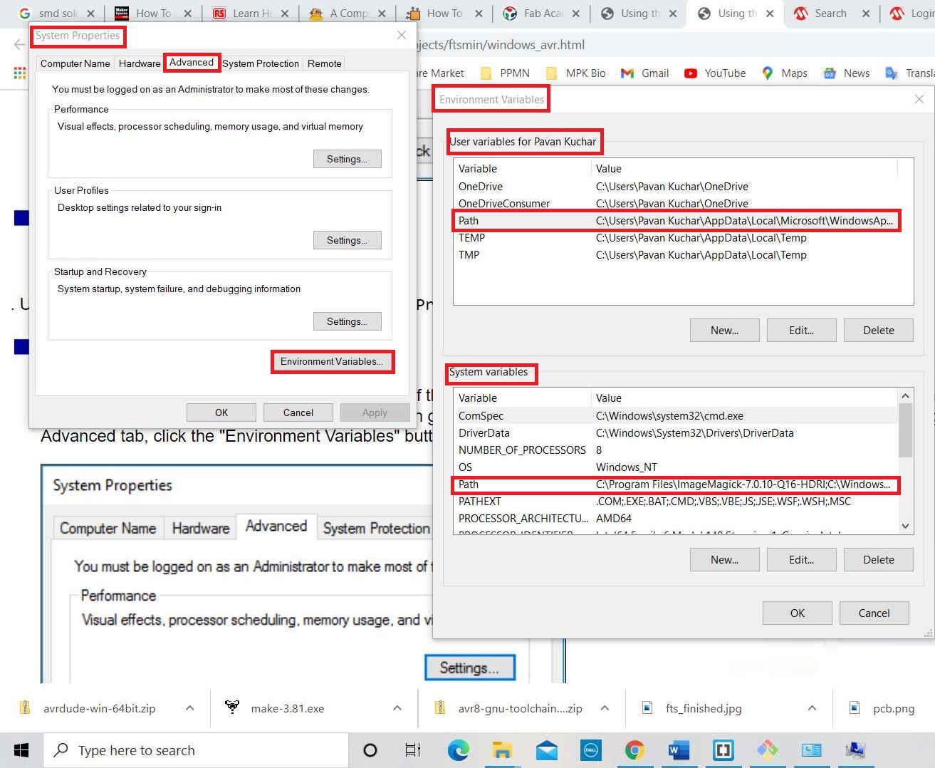
The Screenshots of the AVR Dude Toolchain, AVR GNU, Make and Adafruit drivers installation process on my Laptop are given below.
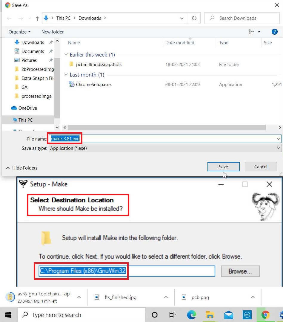
Downloading Make
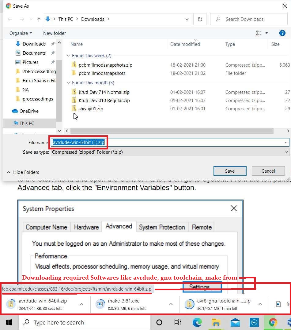
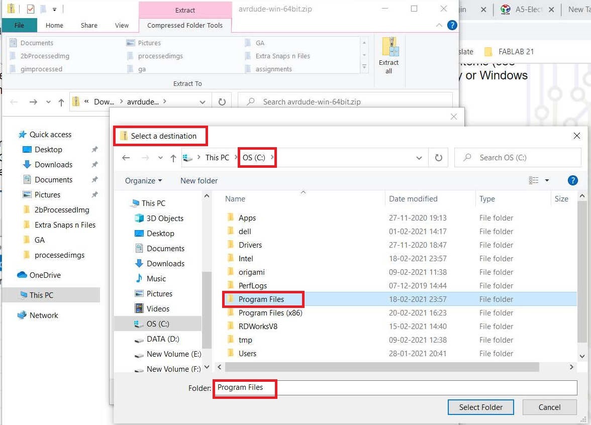
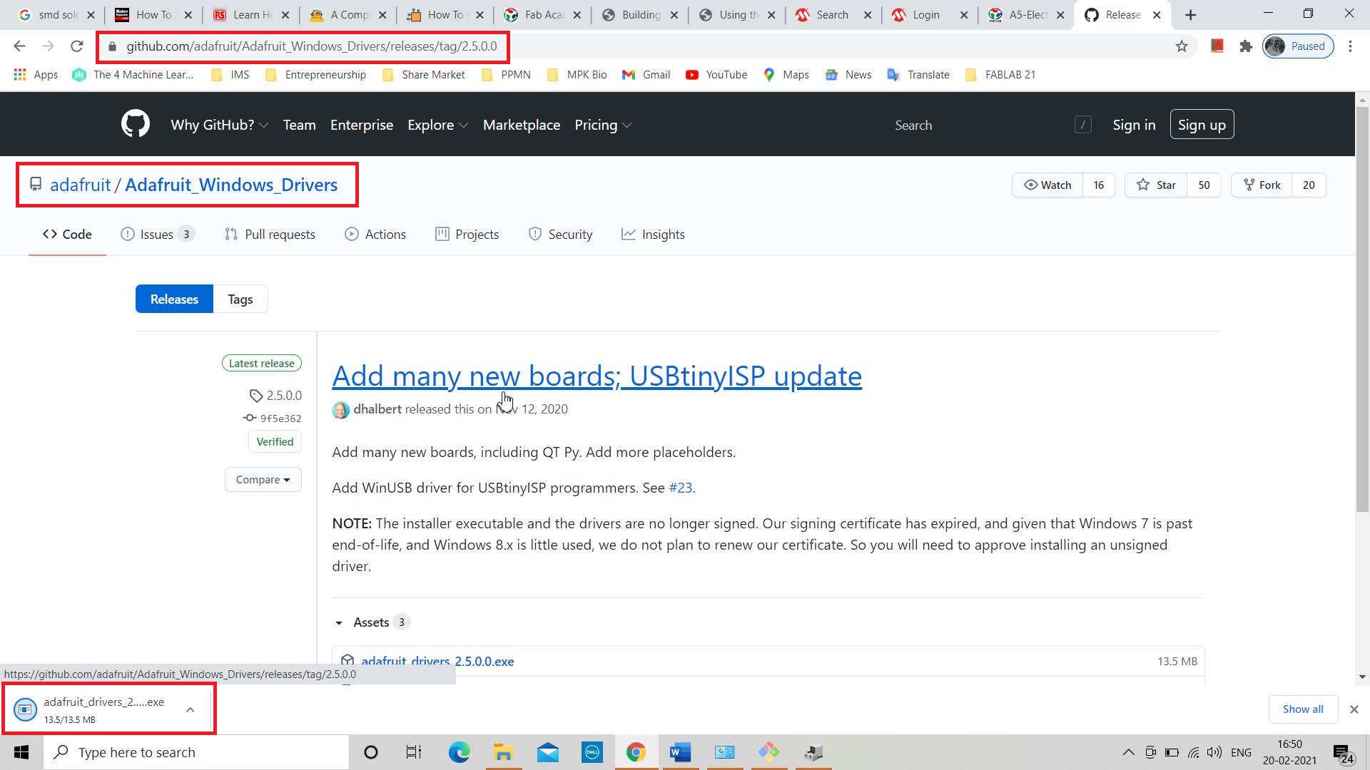
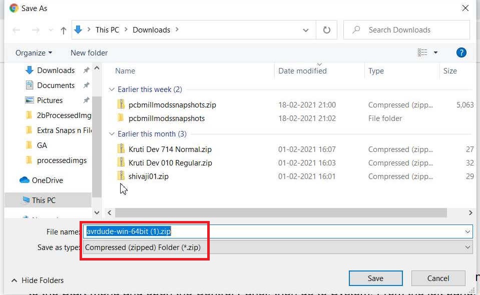
Downloading avrdude
Defining Path for installing the software
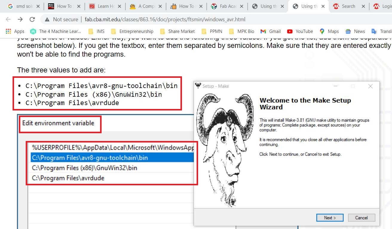
Make Setup Done
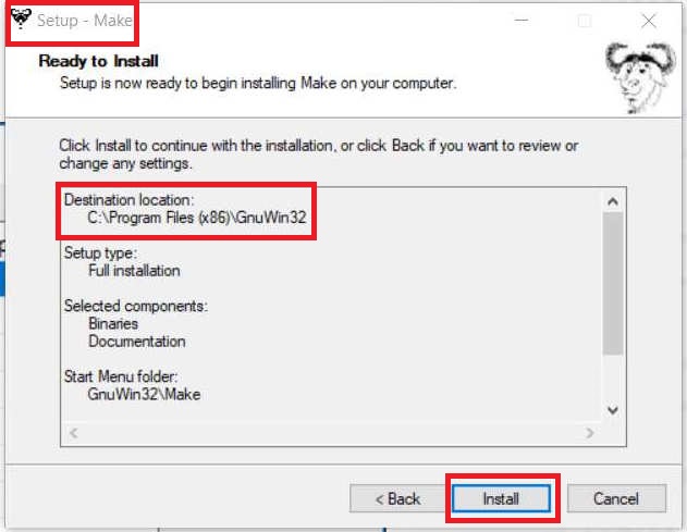
Make succesfully installed
Defined the Location of make setup
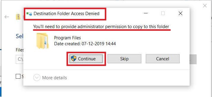
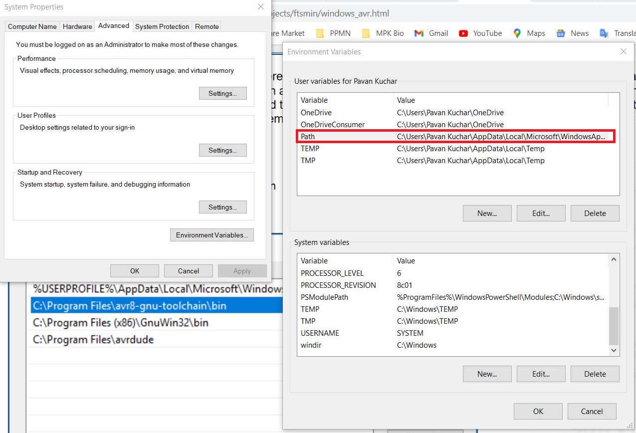
Provided the Admin permission for making changes
Changed the path
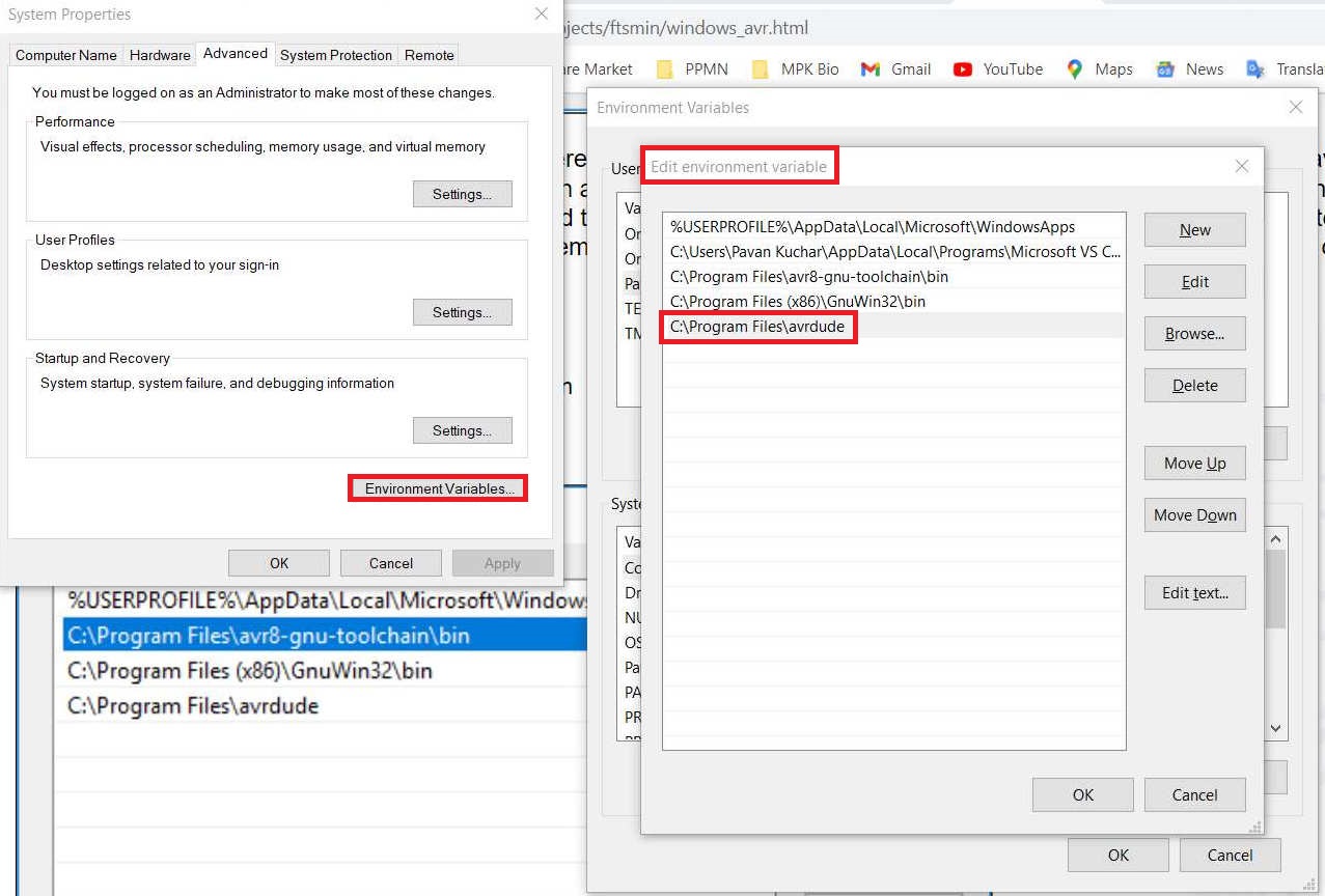
New Path is generated
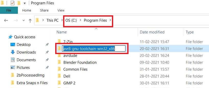
Changed the File Name
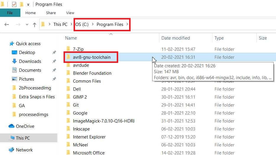
Deleted _x86 from the File Name
Stated gitbash
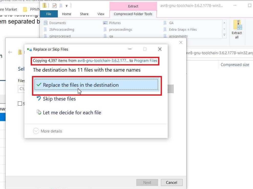
avr GNU Toolchain processed
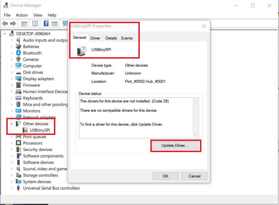
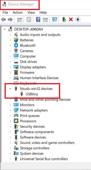
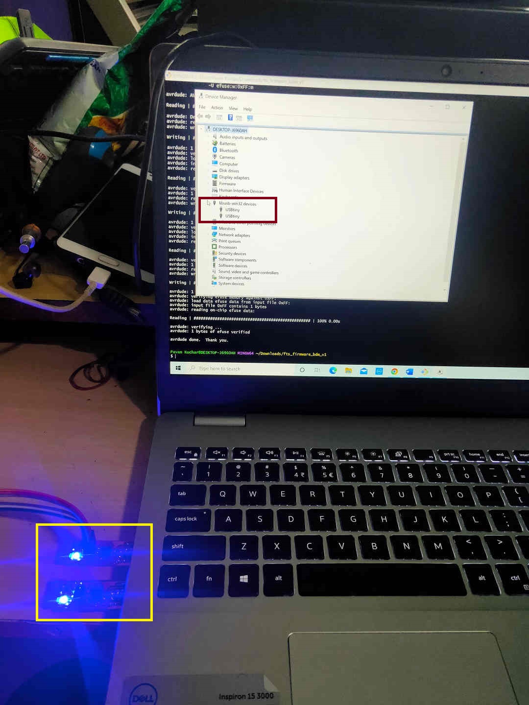
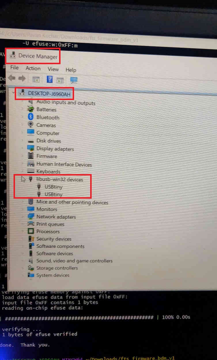
USB tiny programmer
The .hex file could be found here.
in HEX file change to USB tiny
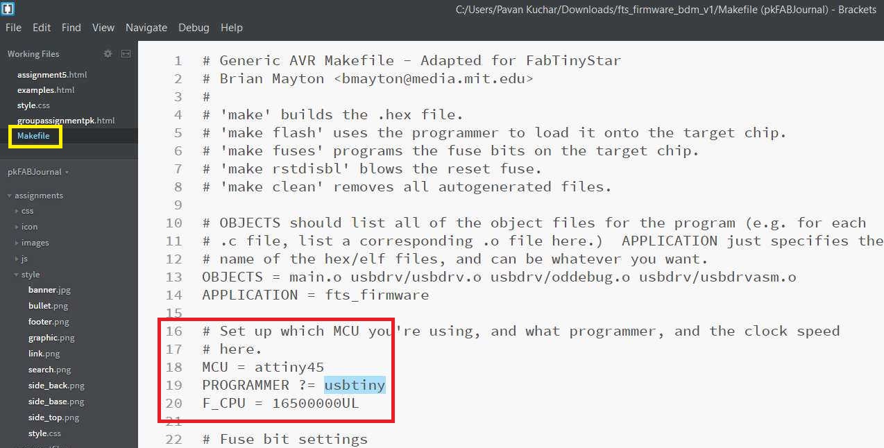
Firmware download
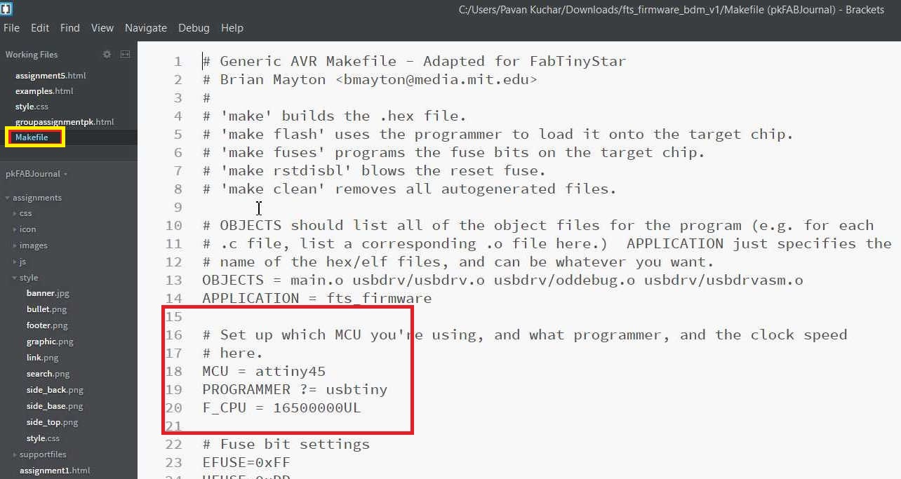
Configure the Firware
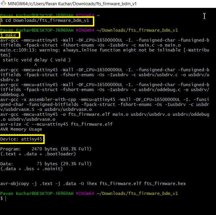
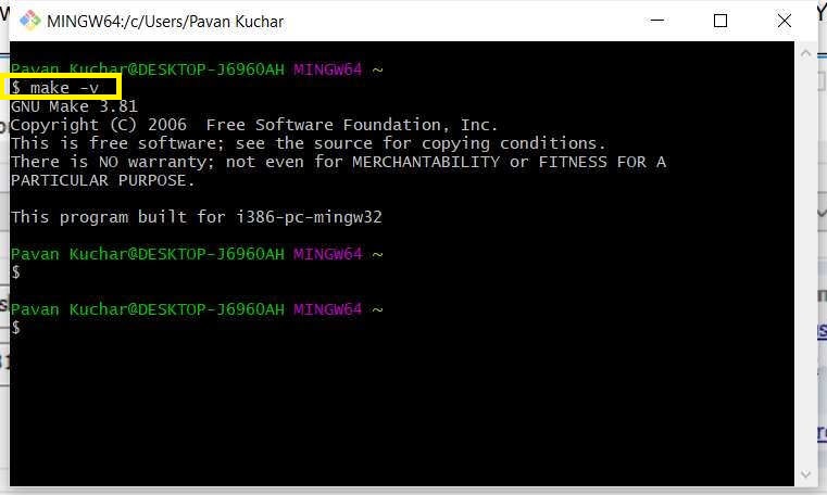
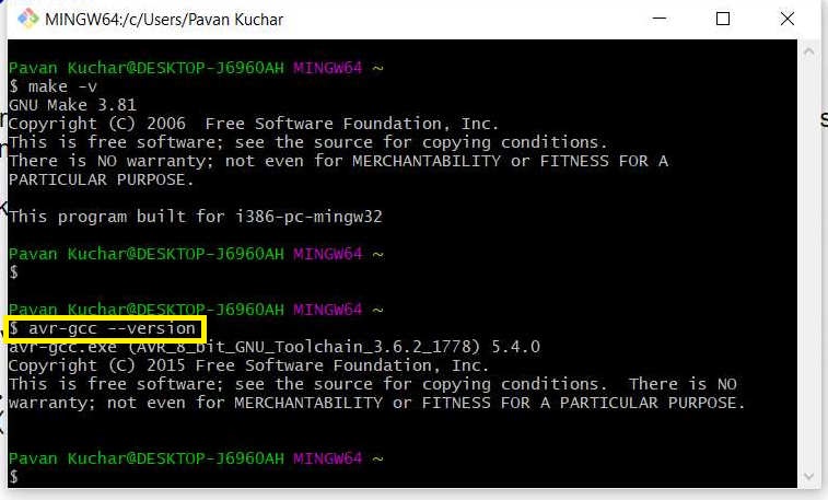
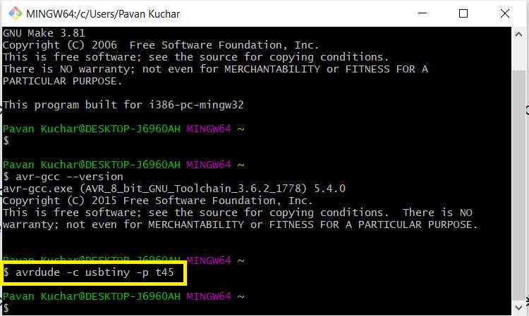
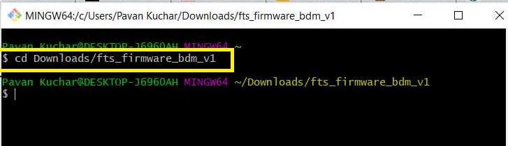
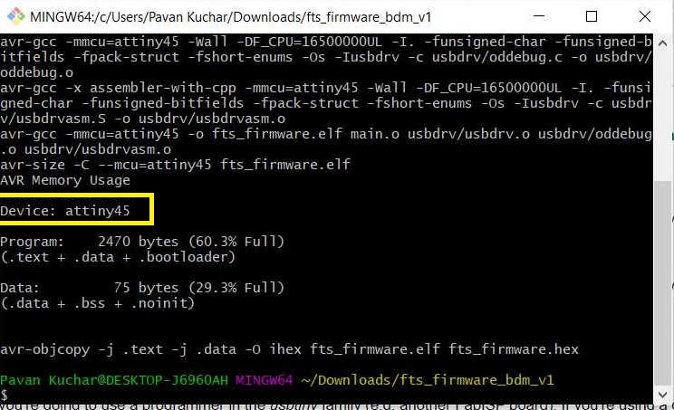
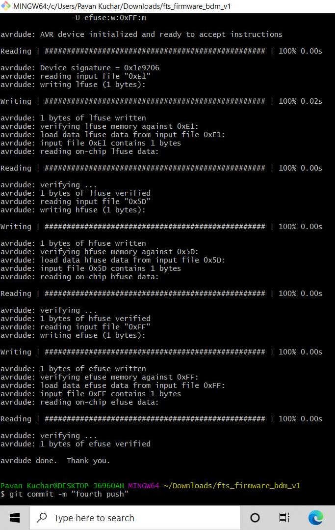
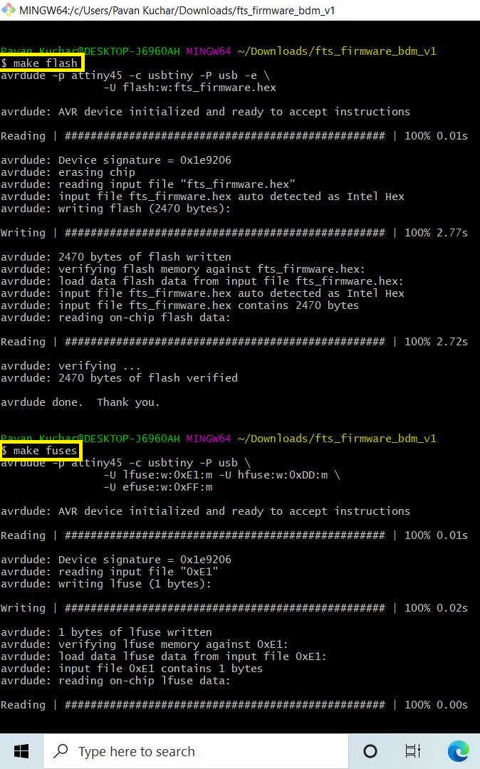
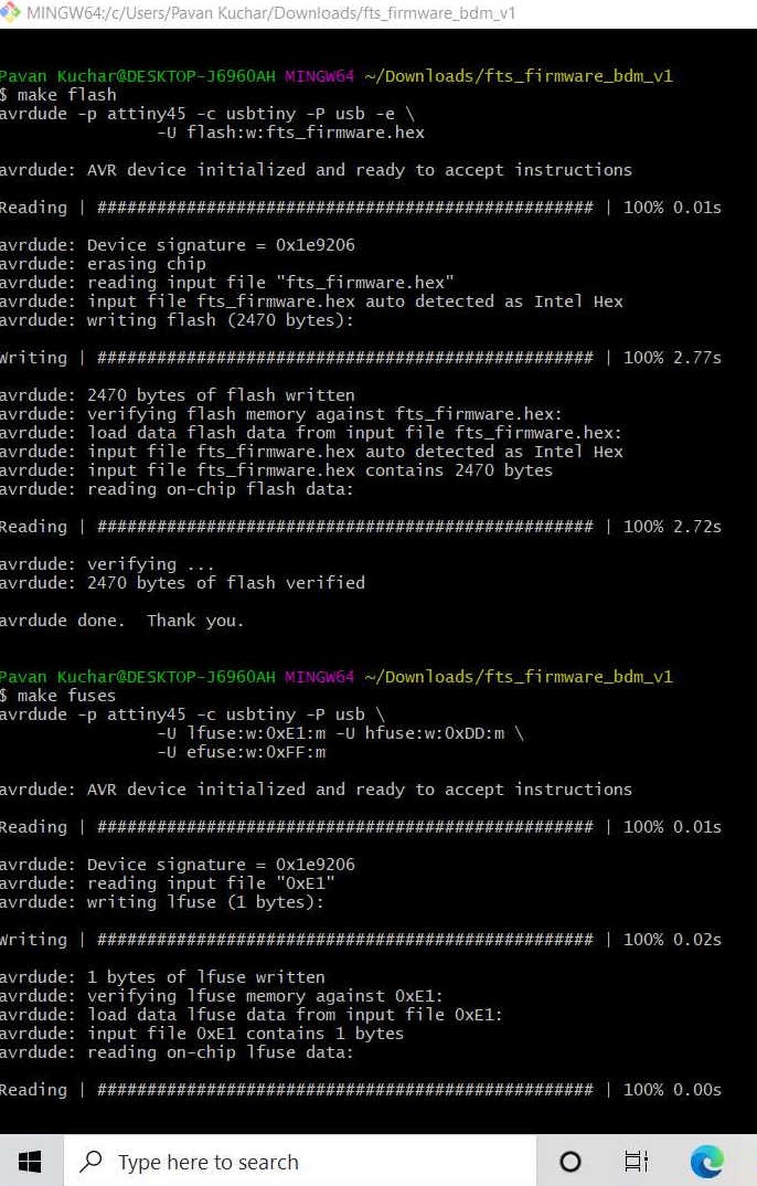
The various commands used by me in Git Bash for programming the PCB plate (Fab ISP) are:
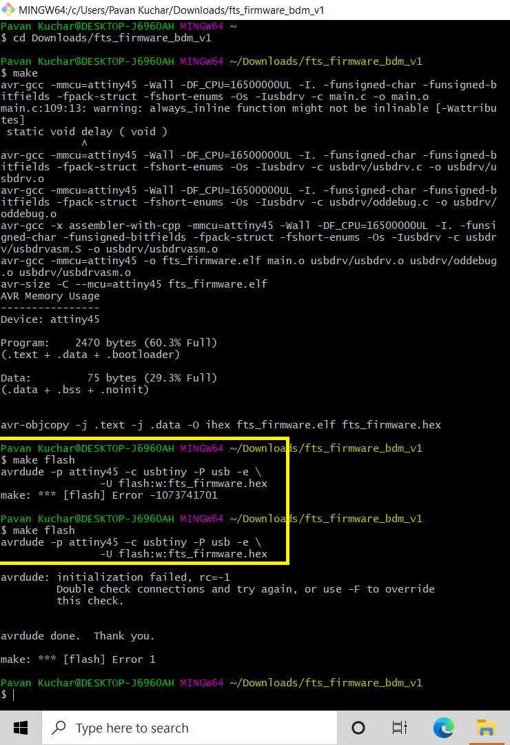
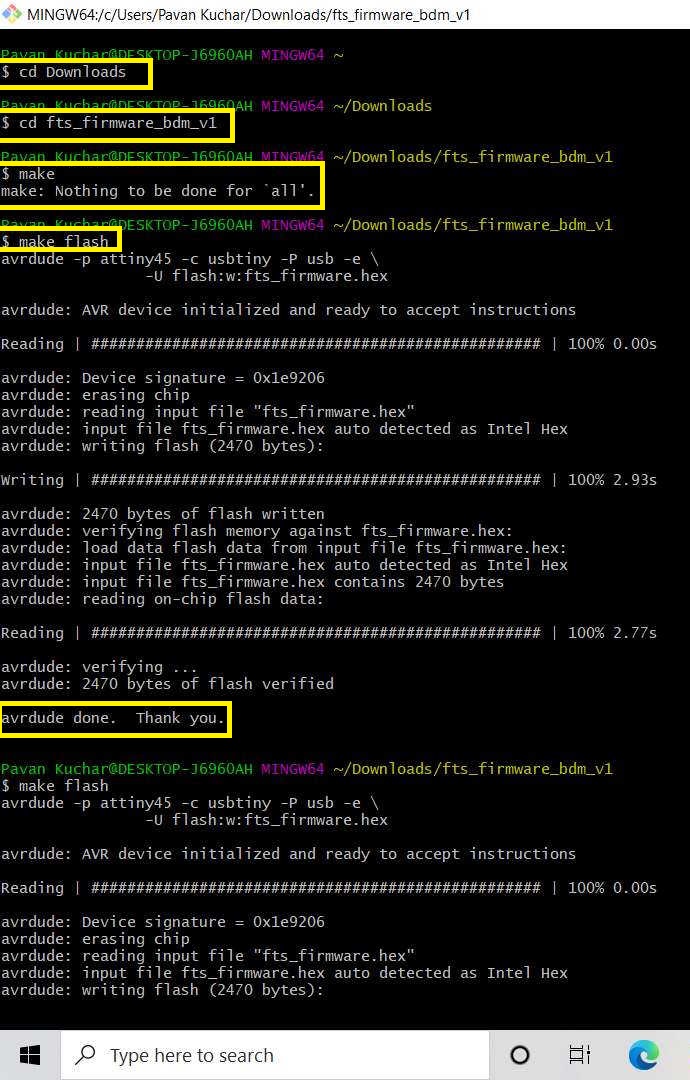
used make command
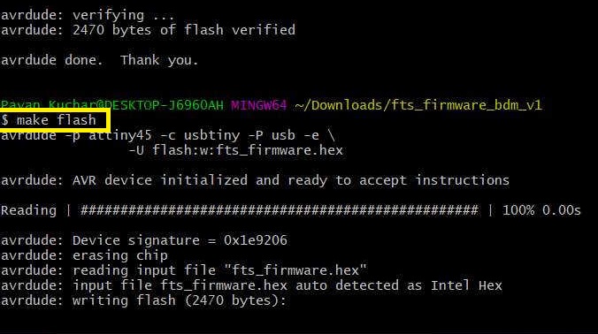
used make flash command
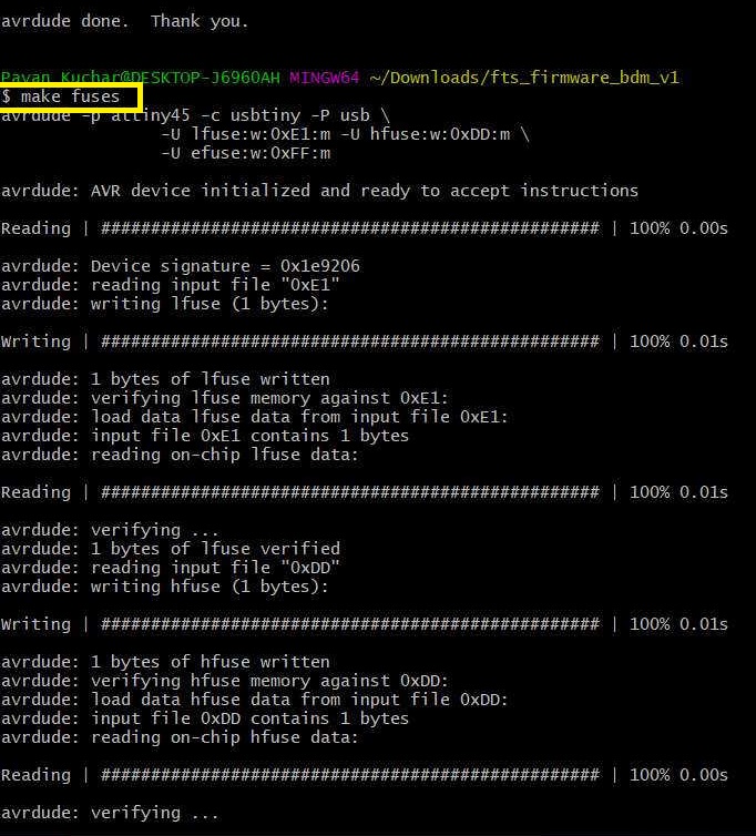
used make fuses command
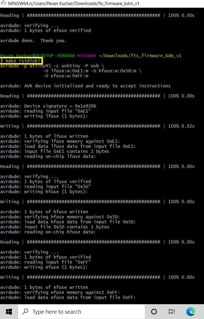
used make rstdisbl command
configuration process ongoing and completed the setup
I prepared two ATtiny45 programmers. So, applied the same process to make it programmable.
used make fuses command
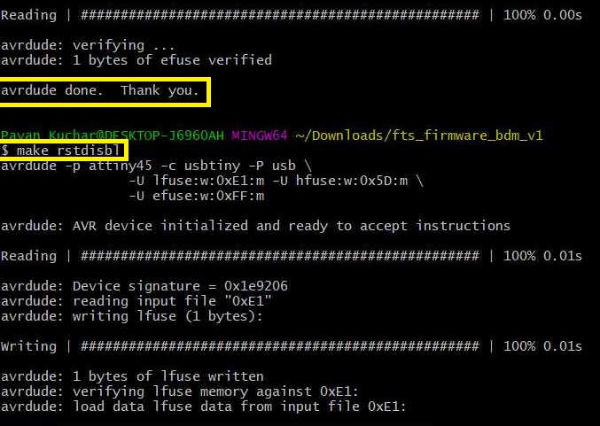
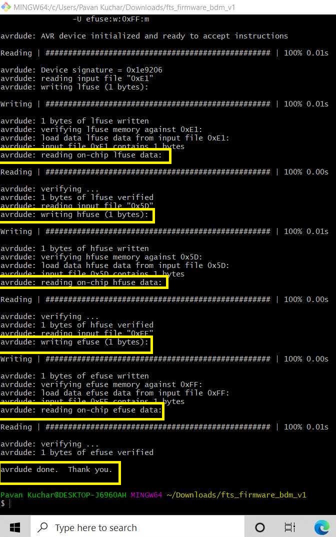
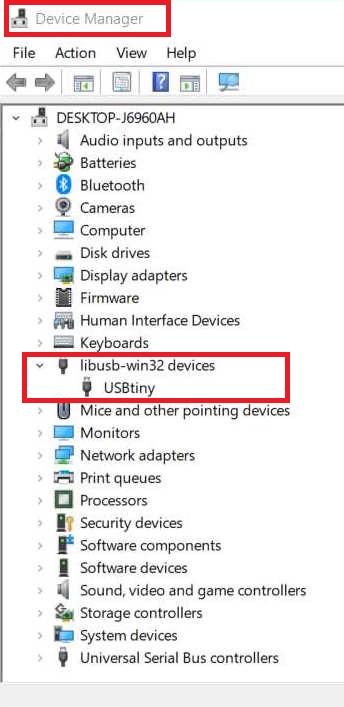
After the installation of AVR Dude, GNU, Make and adafruit drivers, I then used Git Bash for programming the PCB plate (FAB ISP) fabricated by me earlier. The Screenshots of this process are given below.
Issues during programming the Fab ISP faced by me:
I then downloaded the FFMPEG for Windows to Compress the size and trim the length of the Video. I used the commands given in CAD Design Week here.
Video Stream of the LED's Flashing while programming the Fab ISP:
Downloads:
The Original Design Files of PCB Trace Cut of Brian FABISP, Test as well as the .HEX file can be downloaded from here.