How to make (almost) anything.
Week 13. Networking and communications.
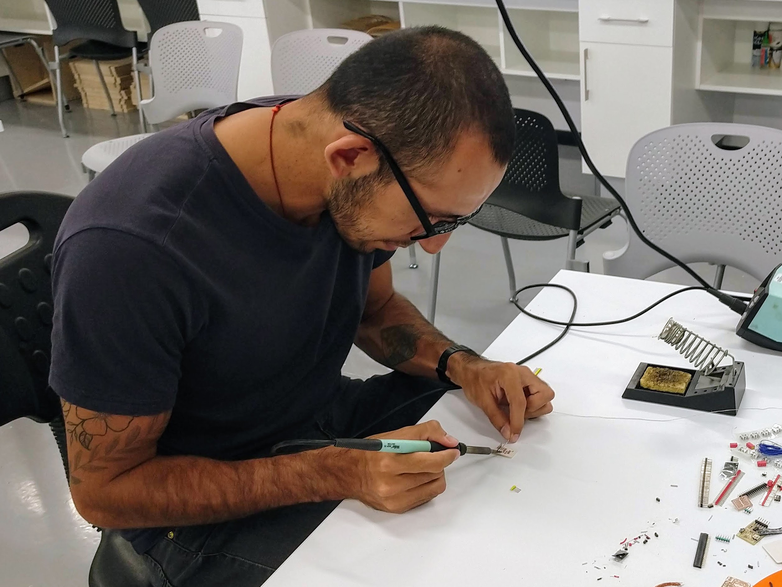
Work done in the Lab under the guidance of my remote Instructor to accomplish the weekly assignments.
This week I made a network of master and slave boards to power some LEDs.
Group assignment
This week we sent a message between two projects, you can read it there.
Communication protocols on Arduino
As I am quite satisfied with the board I made for my final project, I decided to test it by sending orders to other commercial boards using one of the three communication protocols available on Arduino: UART, I2C and SPI. At first I did not understand any of the terms but reading different tutorials (this one from Device Plus explains from the basics the differences between the protocols ), I chose UART for its ease of use as it was my first project that involves networks.
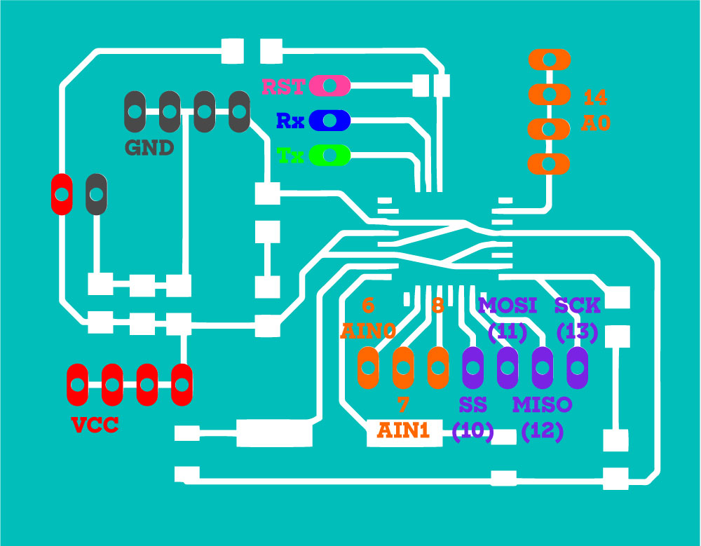
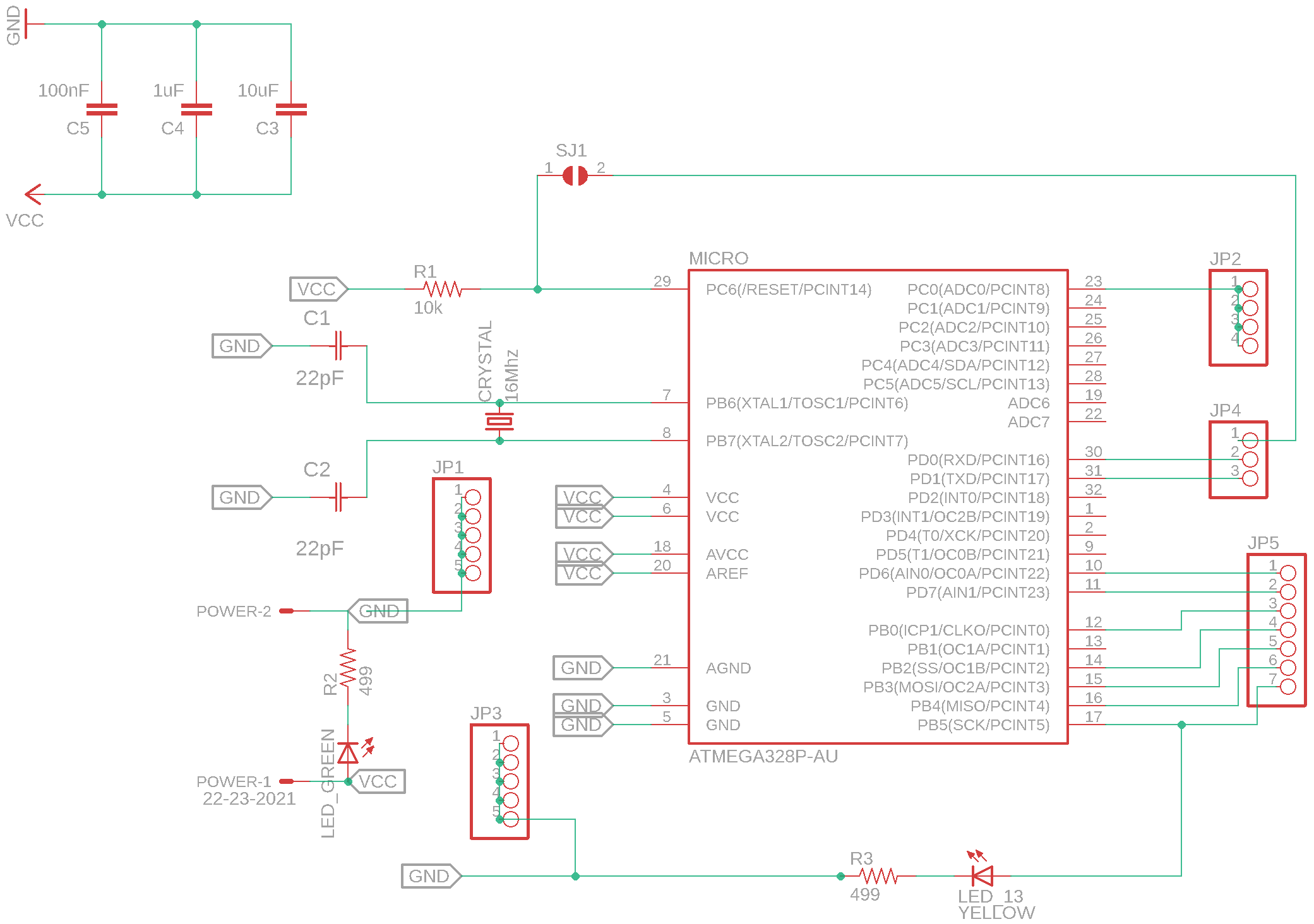
The pins on my ATmega328P board are these:
>
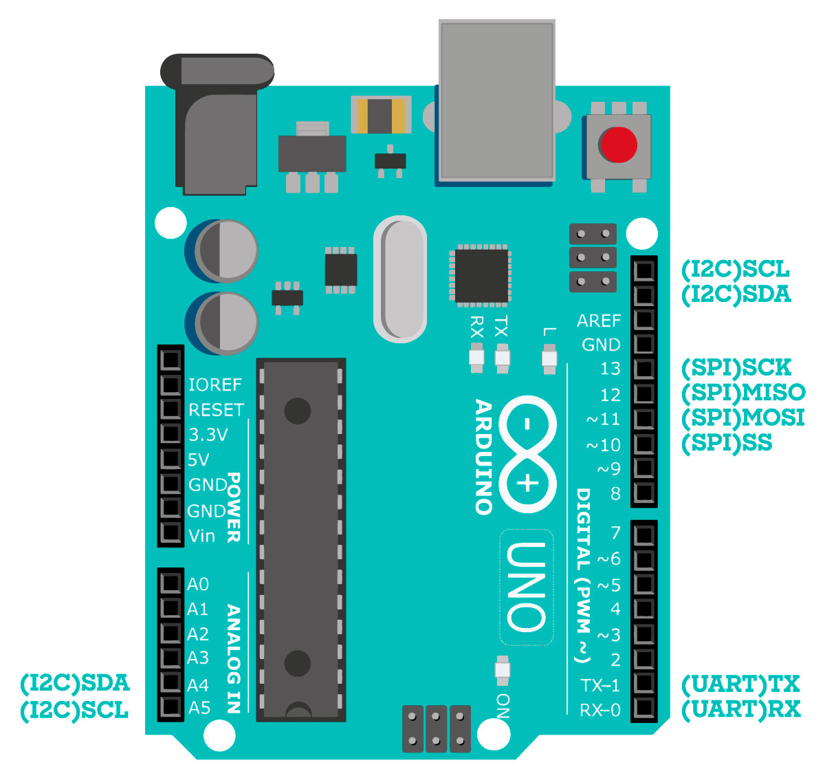
The networking pins on Arduino UNO are these:
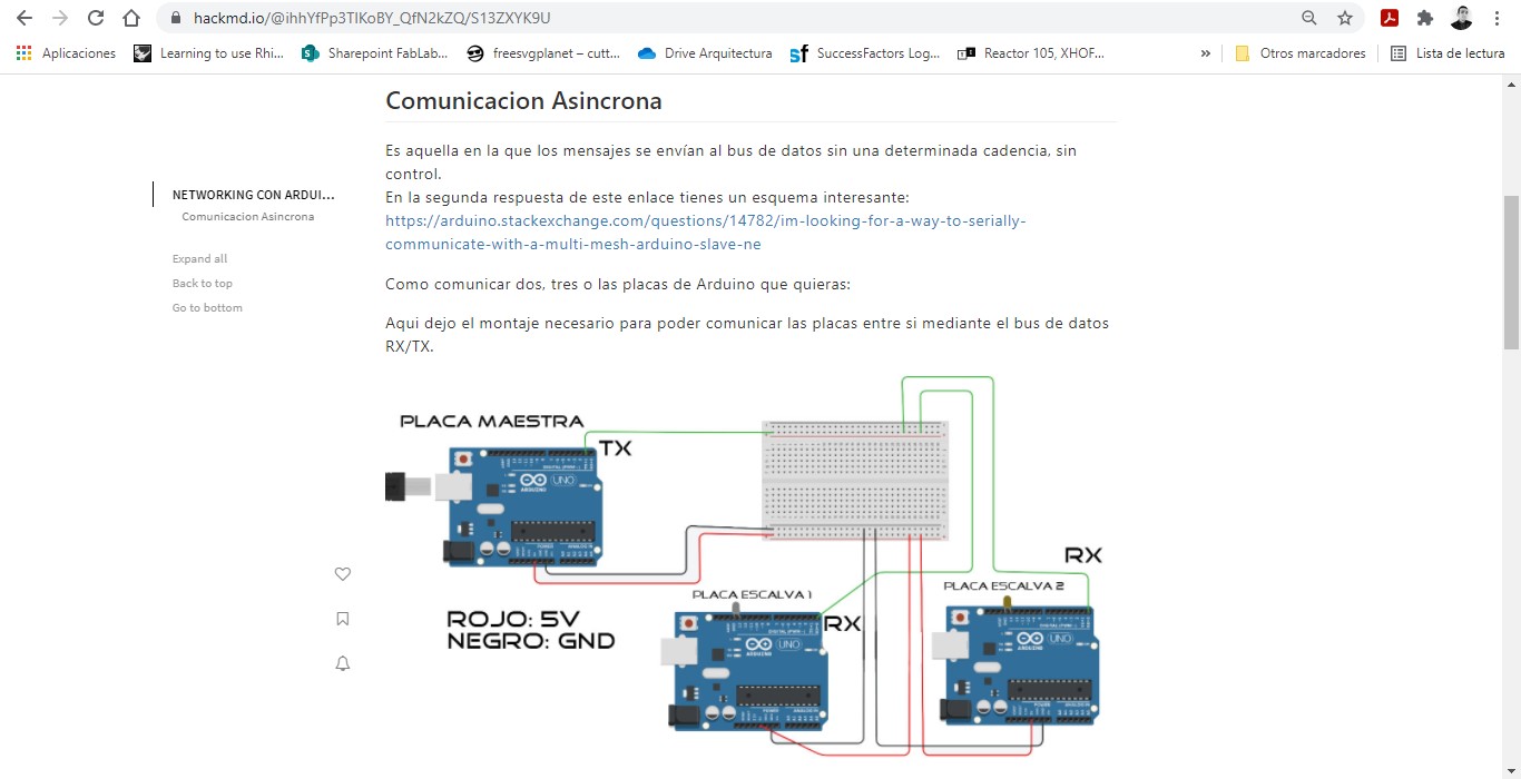
The Universal Asynchronous Receiver/Transmitter (UART)
A basic UART system provides robust, moderate-speed two-way communication with just three signals: Tx (transmitted serial data), Rx (received serial data), and ground. Unlike other protocols like SPI and I2C, no clock signal is required because the user provides the UART hardware with the necessary timing information.
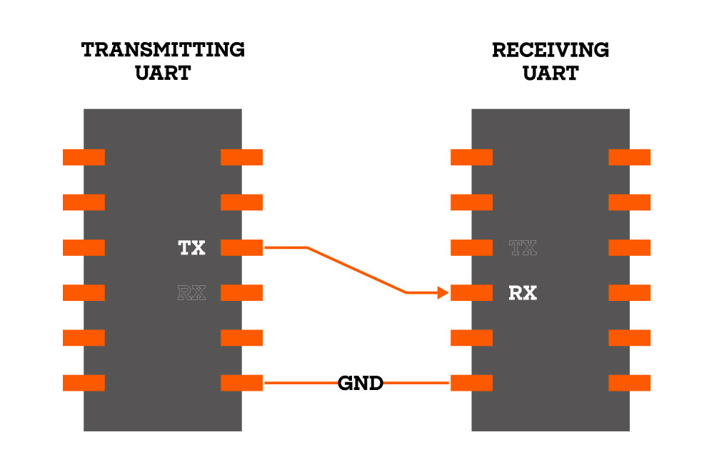
There is actually a clock signal, but it is not transmitted from one communication device to the other; rather, both the receiver and the transmitter have internal clock signals that govern how changing logic levels are generated (on the Tx side) and interpreted (on the Rx side). Unsurprisingly, UART communication does not work if the transmitter and receiver have been configured for different frequencies of data transmission.
Pablo Nuñez has a short but extremely useful tutorial on Arduino communication via UART (Universal Asynchronous Receiver / Transmitter). I followed the tutorial and everything worked correctly: a master board writes two different names on the serial port sequentially and two slave boards have one of those names assigned, when their name is written the board lights the LED attached.
As I wanted to be the one who had control of the orders that were executed from the master board to the slave I added an input device: I modified Pablo's example to implement a button press signal instead of an automatic naming sequence.
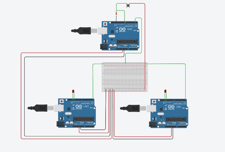
When the button is pressed, the name of one of the boards is written to the serial port, the slave boards have different names assigned so when they are "called" from the serial port, they perform an action through an output pin, in this example they turn on its own LED (but it could be any output device).
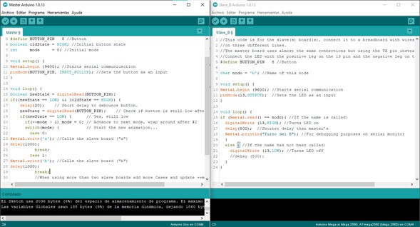
Master board code:
//This code is for the master board, connect it to a breadboard with wires on TX, 5V and GND
//on three different lines.
//The slave(s) board(s) uses almost the same connections but using the RX pin instead.
//Connect the LED with the positive leg on the 13 pin and the negative leg on the next pin (GND).
#define BUTTON_PIN   8 //Button
boolean oldState = HIGH; //Initial button state
int     mode     = 0; //Initial mode

void setup() {
Serial.begin (9600); //Starts serial monitor
pinMode(BUTTON_PIN, INPUT_PULLUP); //Sets the button as an input
}

void loop() {
boolean newState = digitalRead(BUTTON_PIN);
if((newState == LOW) && (oldState == HIGH)) {
    delay(20);    // Short delay to debounce button.
    newState = digitalRead(BUTTON_PIN);    // Check if button is still low after debounce.
    if(newState == LOW) {      // Yes, still low
      if(++mode > 1) mode = 0; // Advance to next mode, wrap around after #2
      switch(mode) {           // Start the new animation...
        case 0:
Serial.write('a'); //Calls the slave board ("a")
delay(1000);
          break;
        case 1:
Serial.write('b'); //Calls the slave board ("b")
delay(1000);
          break;
          //When using more than two slave boards add more Cases and update ++mode > 1 on line 20
      }
      }
    }
      oldState = newState; //Update the button state
}
Slave board(s) code:
//This code is for the slave(s) board(s), connect it to a breadboard with wires on RX, 5V and GND
//on three different lines.
//The master board uses almost the same connections but using the TX pin instead.
//Connect the LED with the positive leg on the 13 pin and the negative leg on the next pin (GND).
#define BUTTON_PIN   8 //Button

char nodo = 'b'; //Name of this node

void setup() {
Serial.begin (9600); //Starts serial communication
pinMode(13,OUTPUT);  //Sets the LED as an input
}

void loop() {
if (Serial.read() == nodo){ //If the name is called:
  digitalWrite (13,HIGH); //Turns LED on
  delay(500);  //Shorter delay than master's
  Serial.println("Turno del B"); //For debugging purposes on serial monitor
  }
  else { //If the name has not been called:
    digitalWrite (13,LOW); //Turns LED off
    //delay (500);
  }
}
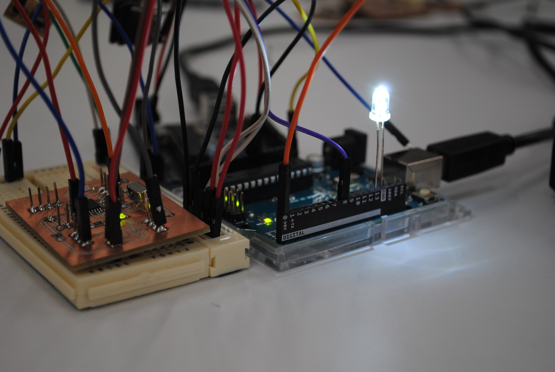
In this video the Arduino board on the left is the master and receives the signal from the button, it uses its Tx port to transmit a signal to the two boards on the right that are the slaves and they turn on their LEDs when it is their turn.
On my own board the Rx and Tx pins are enabled on 16 and 17, so it can work as a master to control other boards.
The real purpose of this was to control the Arduino UNO boards using my own ATmega328p board. In this video I replaced the master Arduino board with my board to test that the Rx and Tx ports were working properly with the same code, and everything went as it should.
Master with button as input: Chonikit v3 (at the left). Slaves with LEDs: Arduino UNO (at the right).
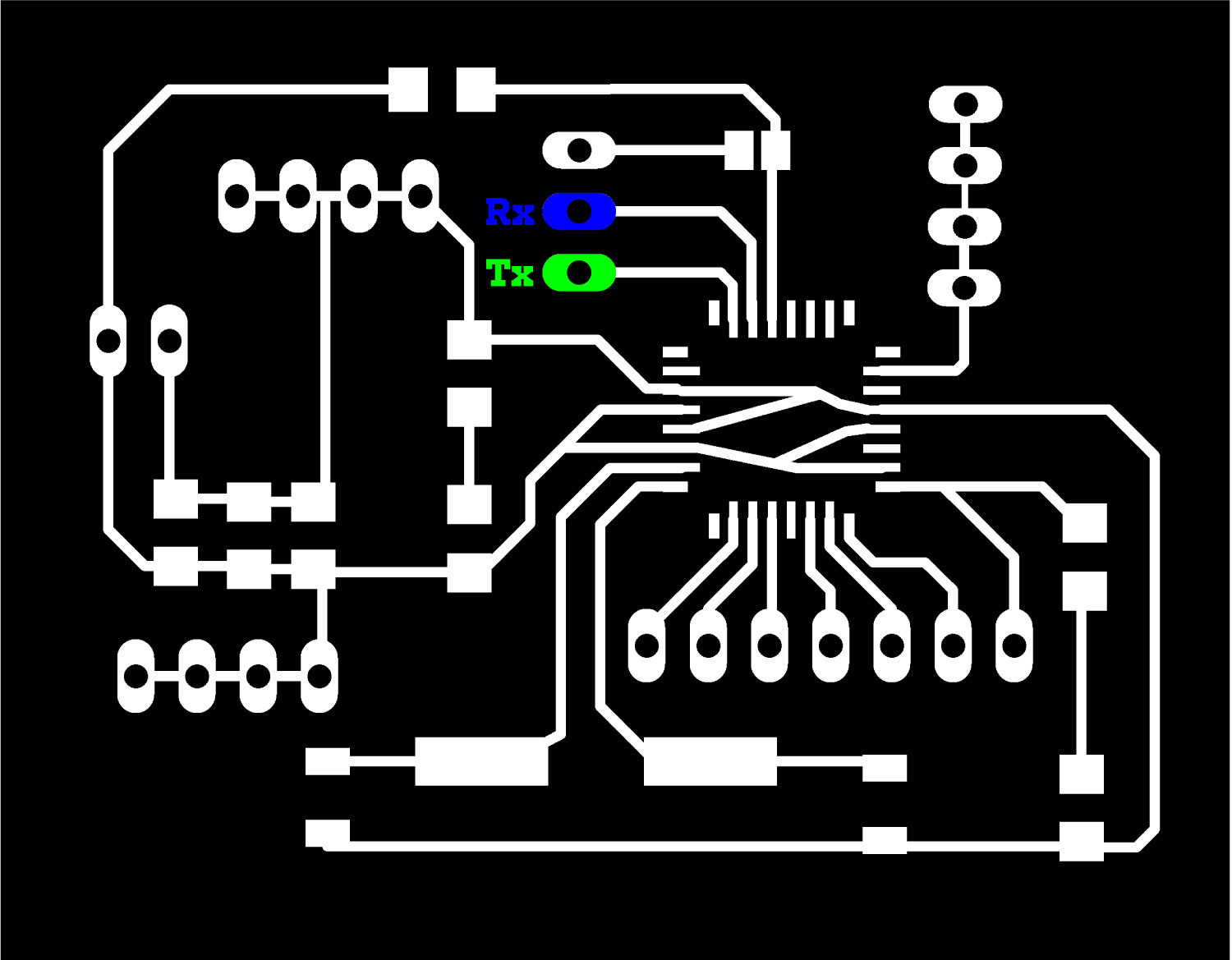
Luis Carvao during my global evaluation reminded me of something that I had not considered: the evaluation guidelines indicate that I cannot use breadboards, so I made a small board to connect the three boards and the button, its pins are labeled with the acronyms GND, VCC, Tx (for the master board) and Rx (for the two slave boards).
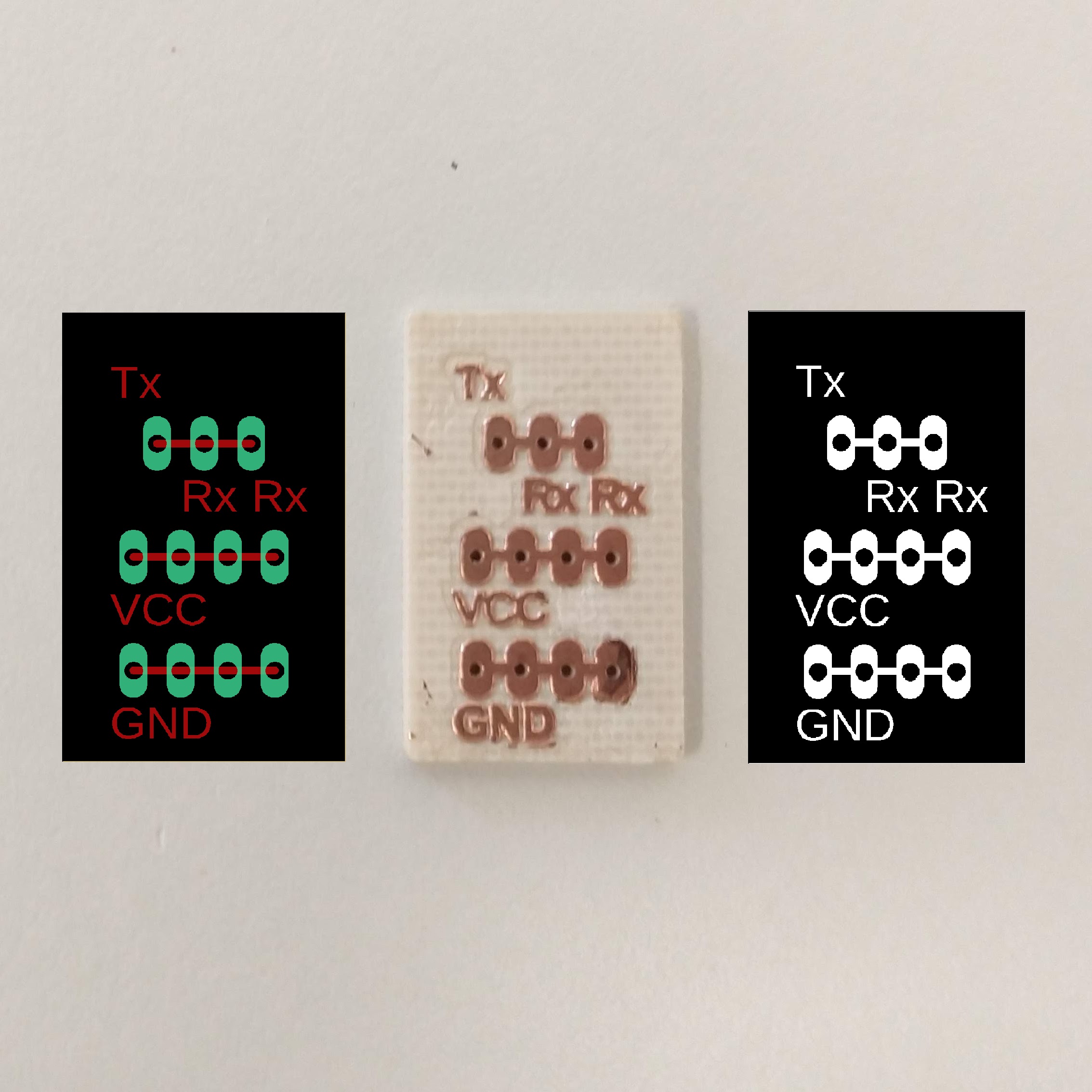
I must admit that the connections are much easier using this board, and all the wiring looks cleaner.
Files
You can download the .INO files here: Master, Slave A, Slave B.
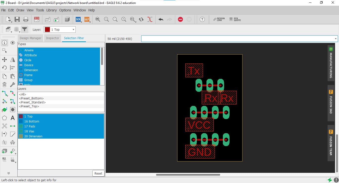
You can download the network adapter board files here: board,schematic.
You can download the ATmega328p board files here: schematic, board.
|
For this assignment I:
|