Electronics Design
ELECTRONICS DESIGN
This is the content we had covered this week:
W6 - Electronics Design
- Components
- Circuits
- Equipment
Assignment
-
Group assignment: Use the test equipment in your lab to observe the operation of a microcontroller circuit board.
-
Individual assignment: Redraw an echo hello-world board, add (at least) a button and LED (with current-limiting resistor) check the design rules, make it, and test it extra credit: simulate its operation.
This week we’ve been working to create learn how to design circuits from sratch using EDA software. We covered some principles on electronics as well.
HOW TO DESIGN A CIRCUIT
ELECTRONICS BASICS
Even though I had worked with electronics before, I never had such an in-depth overview of what are genuinely grounding fundamentals. These diagrams summarize all I want to remember for the various components and their functioning and properties.
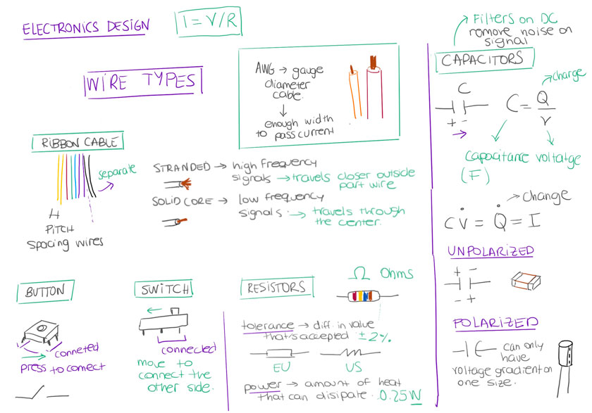
"Diagram showing some Electronics Basics"
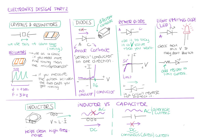
"Diagram showing some Electronics Basics"
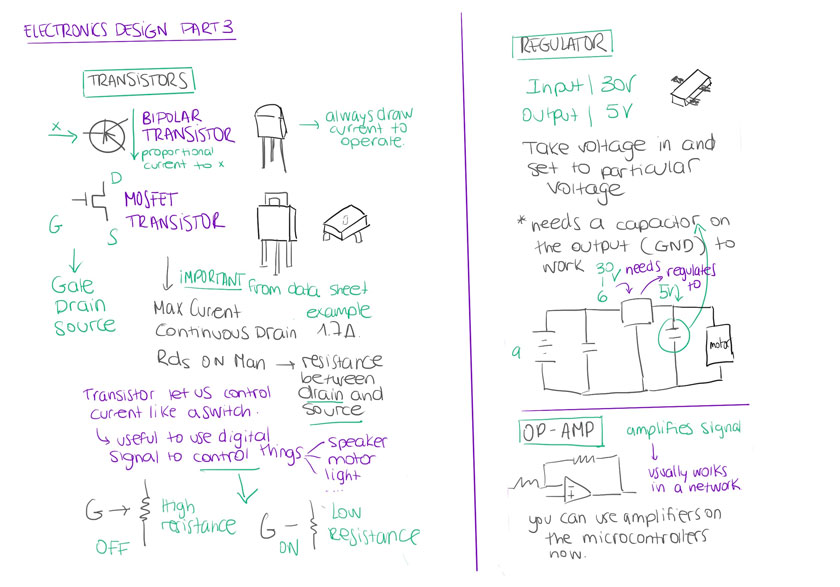
"Diagram showing some Electronics Basics"
CIRCUITS
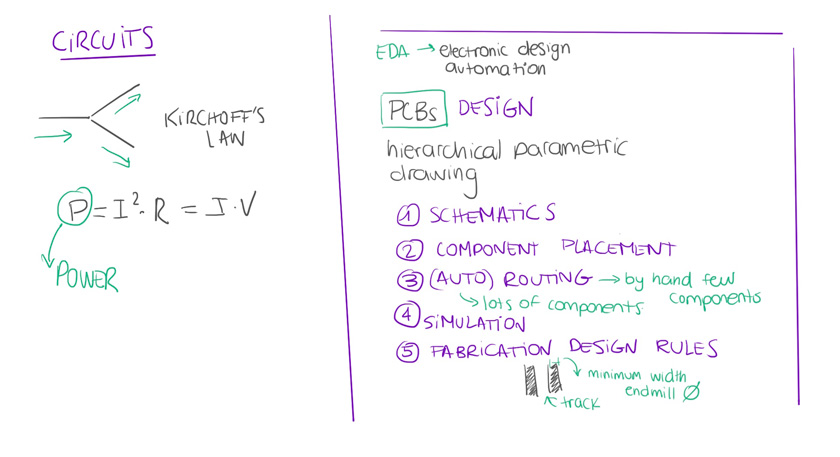
"Diagram showing circuits design basics"
HOW TO DESIGN A CIRCUIT?
GROUP ASSIGNMENT
This week we had to to test the different lab tools. In this case, we had a conversation we some peers and I decided to go on my own trying to learn more about the tools.
DIGITAL MULTIMETER
This is the tools I’m using the most to check continuity, resistance, capacitance,…
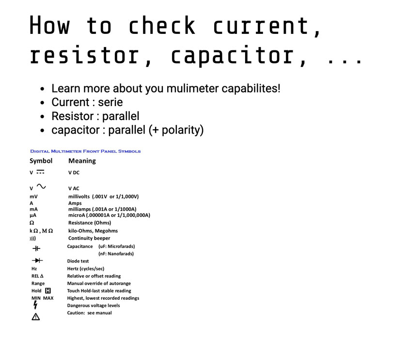
"Image showing how to check everything using a multimeter ( From debugging recitation)."
Here some images checking my assignment:
"LEFT: Soldering test. RIGHT: Testing Diode with multimeter."
At every step I had my multimeter at a hand to check continuity. As the circuit seemed delicate I paid special attention at this.
"LEFT: Checking LED's resistor. RIGHT: Checking Buttons external pull-up resistor."
OSCILLOSCOPE
The one we have at the lab is not working at the moment. Therefore I watched the recitation that explains how to use it. I hope to test it soon.
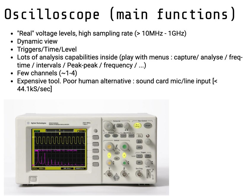
"Image showing an oscilloscope with its main functions."
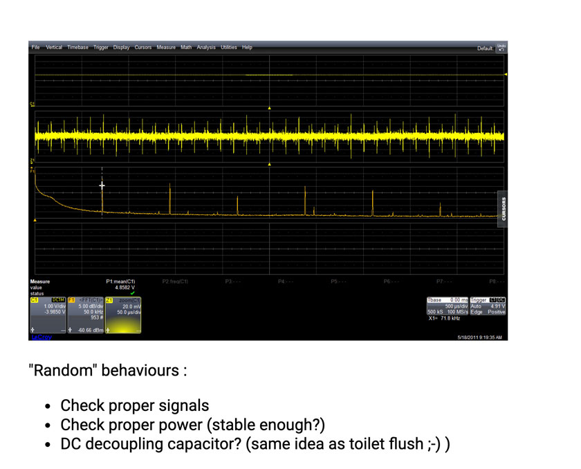
"Image showing how to read a signal on the oscilloscope."
We have the Seeds DSO Nano v3 handheld Oscilloscope, but I couldn’t figure out how it works beyond connecting it to a 3V battery and seeing a change on the signal.
REGULATED POWER SUPPLY
I couldn’t use it this week either. However I was able to choose a proper power source for my circuit.
WHAT WENT WELL
Better understanding: With more understanding of the electronics components, it comes with more understanding of how to use the tools to check them.
Future uses: Even though I couldn’t test all the tools, I’m ready to try more features in the future.
WHAT COULD BE BETTER
Not all available:Given that some tools weren’t working I got more theoretical knowledge that practical one.
Some gaps: I still have some gaps to fully understand the usage of some features, mainly oscilloscope.
INDIVIDUAL ASSIGNMENT
I wanted to design my circuit from scratch, that’s why I went for a simple option that could help me learn and at the same time achieve my goal. As the minimum requirements were a button + LED, I decided to use an Attiny 45 to create my design. Also, I wanted it to be FLEXIBLE!.
1. CHOOSE MICROCONTROLLER | Attiny 45
First I checked the pinout for the microcrontroller I wanted to use before designing my circuit.
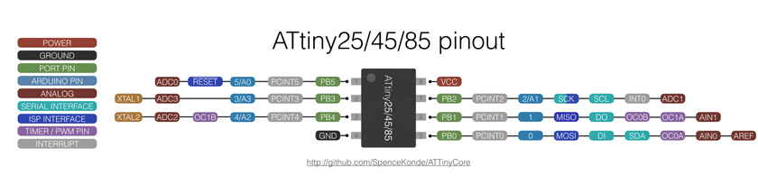
"Image showing the pinout for the Attiny 45 that I want to use."
2.SKETCH CIRCUIT
Before sketching the circuit I had to check the pinout of the Attiny45 to decide which pins to use. Even though the focus of this week wasn’t programming the board, I knew I wanted to have a fading LED which needed a PWM pin on my Attiny45. Checking the Attiny45 documentation I picked Arduino Pin 0, which maps to the physical pin 5 on the microcontroller. For the button, I chose physical pin 7, which is Arduino Pin 2.
I draw a very simple sketch of my circuit to make sure I knew what I was doing:
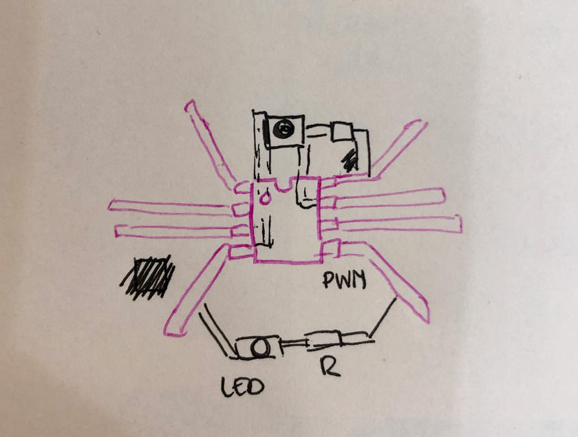
"Image showing a sketch of the simple circuit I want to create."
CHOOSING PROPER COMPONENTS
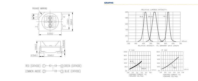
"LEFT: RGB Led Pinout from the datasheet. RIGHT: Intensity graph from datasheet to check current vs voltage. "
For the second board I changed to a clear gren LED that would fit better with my design.
"Clear LED specs from the datasheet. "
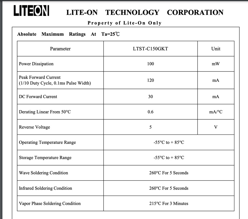
Even though I was planning on using a 3V lithium button battery to power the board, and therefore the LED, I went on the safe side after applying Ohm’s law and the stock we had available at the lab, so I chose a 220 Ohm resistor. If I were to use 5V instead, I’d be safe as well.
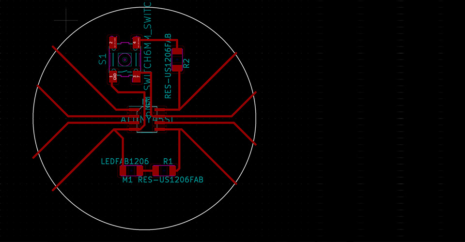
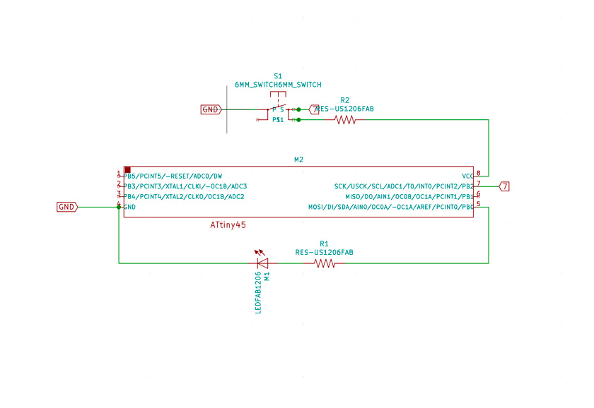
3.KICAD SCHEMATIC LAYOUT EDITOR
I created my schematic using all Fab schematic components. Having a curated list of components helped a lot to navigate hundreds of components.
"Image showing a schematic layout of my circuit using Kicad."
Download Kicad schematic file;
4.KICAD GENERATE NETLIST
Creating netlist to connect the schematics to the footprints and continue on PCB new.
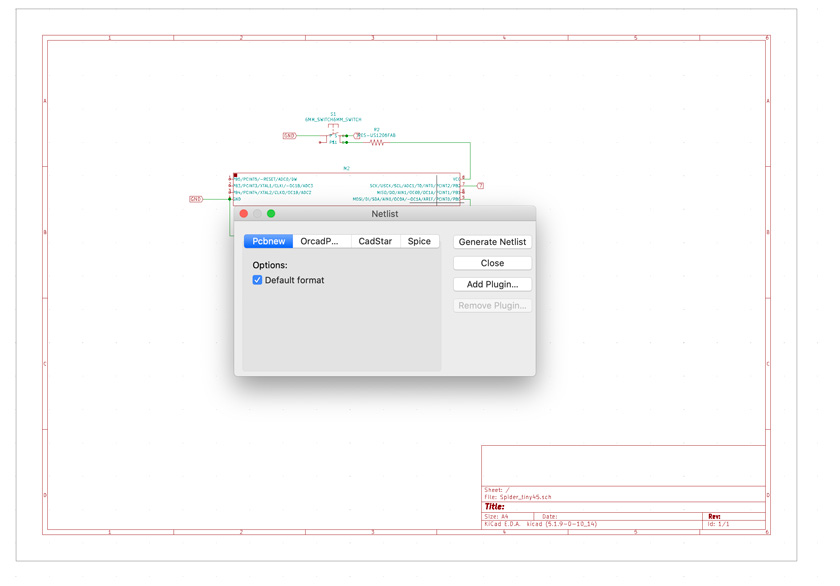
"Image showing the Netlist Generator on Kicad."
5.KICAD PCB NEW + EXPORT
Going from the messy footprints to an organized PCB wasn’t trivial but it ended up working out fine.
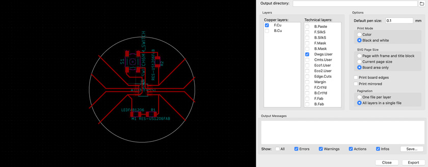
"LEFT: Circuit footprints + routing using design rules. RIGHT: Export settings to .SVG."
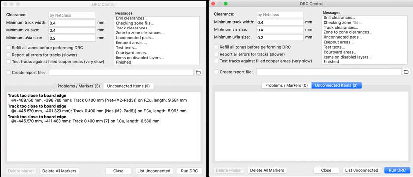
" LEFT: After checking DRC for the first time. RIGHT: Checking DRC after deleting non-problematic markers. All set. "
Download Kicad pro file; Download Kicad pcb file; Download Exported .svg file;
6.ILLUSTRATOR CLEAN-UP + PADS
I didn’t manage to create the half circle pads on Kicad so I continued to finish my PCB on illustrator.
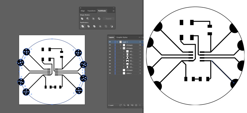
"LEFT: Adding half circular pads to the circuit using Pathfinder boolean operations. RIGHT: Final circuit including pads for aligator clips. "
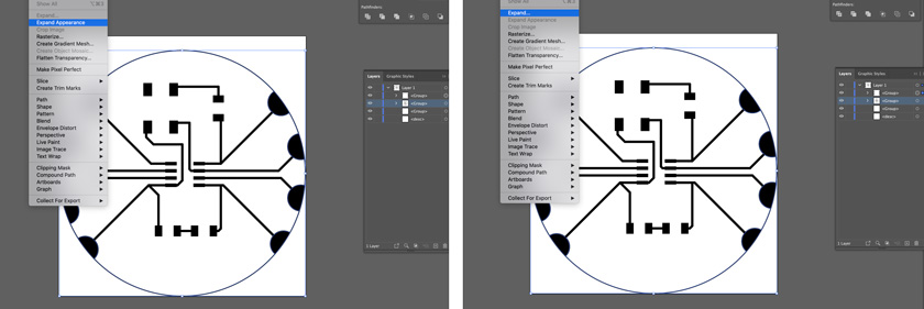
"LEFT: Expand appearance job. RIGHT: Expand fill and stroke to make sure its all one object."
Using illustrator you can export the images to the 1000 dpi needed to mill. But in my case I wasn’t going to use them this week.
A. PRODUCE CIRCUIT | BY HAND
For this assignment, as I was creating a basic circuit I wanted to push myself and try to create a circuit completely by hand.
7A. DRAW CIRCUIT ON PAPER
As I don’t have a printer I draw a larger version of the PCB to be able to craft it by hand.
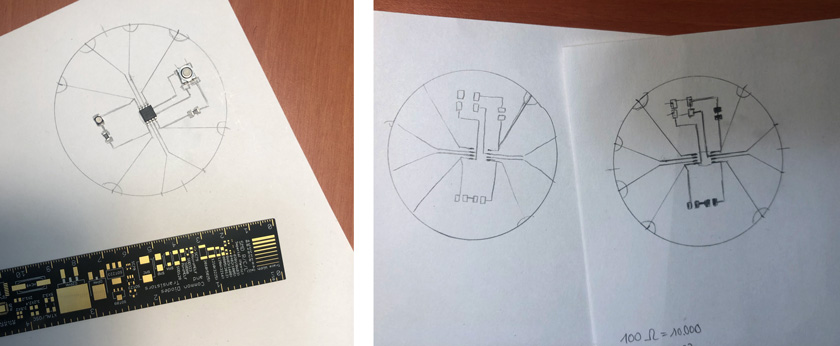
"LEFT: Drawing with Adafruit's PCB ruler. RIGHT: Copy of the drawing to have a back up."
I was helpful to have this ruler to make sure that the components & pads were the proper size.
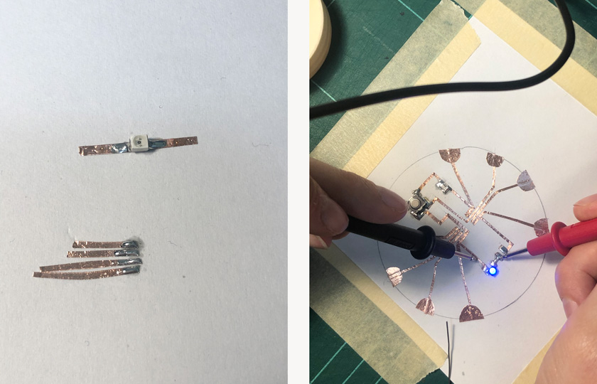
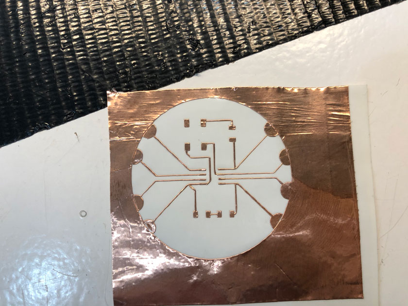
8A. CUT COPPER TAPE PIECES + PRODUCE CIRCUIT
To create the traces I cut even pieces of copper tape to put on tope of the drawing following the traces.
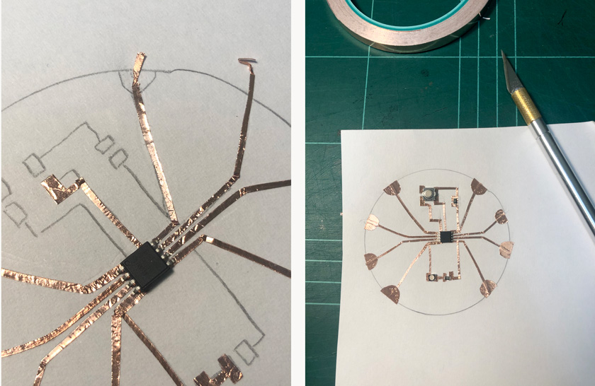
"LEFT: Applying copper strips on the paper. RIGHT: Finished copper tape layer with components on top to check everything is correct."
This part was quite tricky, but extremely rewarding.
9A. TEST SOLDERING + DIODE
I wanted to test soldering on some scraps and spare components to make sure I wasn’t to mess up the real board.
"LEFT: Soldering test. RIGHT: Testing Diode with multimeter."
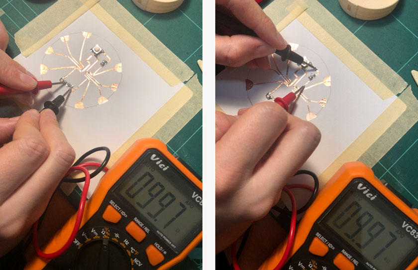
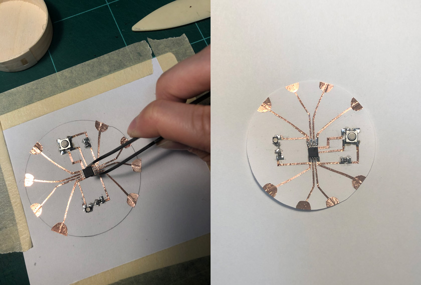
10A. CHECK CONNECTIVITY RESISTORS
At every step I had my multimeter at a hand to check continuity. As the circuit seemed delicate I paid special attention to this.
"LEFT: Checking LED's resistor. RIGHT: Checking Buttons external pull-up resistor."
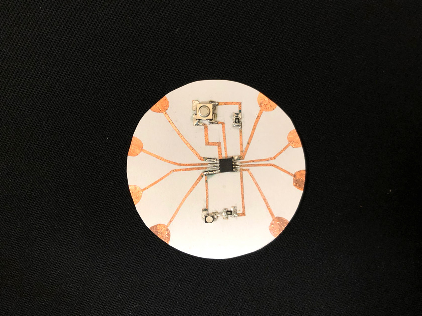
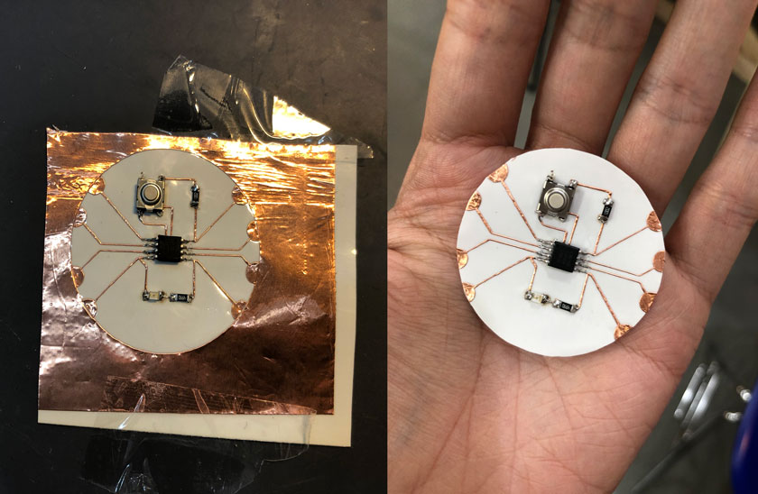
11A. ADD ATTINY 45
Soldering the microcontroller was probably the most nervewrecking moment of the week. I wasn’t sure if I’d be able to solder it without burningthe paper or melting the copper tape. It worked, yay!
"LEFT: Placing Attiny 45 on the circuit. RIGHT: Hand made PCB is done."
CIRCUIT A. FINAL SHOT
"LEFT: Expand appearance job. RIGHT: Expand fill and stroke to make sure its all one object."
WHAT WENT WELL
I had so much fun: I particularly loved the craftmanship of this process.
Very low-res materials: It work using very inexpesive and accessible materials.
WHAT COULD BE BETTER
Better surface:Paper worked fine, but it could be sligthly thicker to absorb better the heat from the soldering iron.
Durability: I know this circuit it will eventually break :(.
B. PRODUCE CIRCUIT | USING VINYL CUTTER
7B. SETUP VINYL CUTTER
As I’ve already used the Roland vinyl cutter, I checked my drawing to follow all the steps.
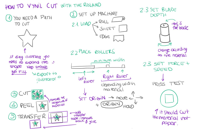
"Diagram showing how the use the Roland Vinyl cutter."
8B. TEST WITH VINYL
As adhesive copper foil is quite expensive, I decided to do some test runs on regular adhesive vinyl. It was a good test to check parameters, and learn how to peel it of without dismanteling the whole circuit.
"LEFT: Vinyl test right after vinyl cutting . RIGHT: Attempt to peel the circuit."
8B. PREP PCB SURFACE
As I wanted to vinyl cut my circuit and copper foil is quite delicate I was advised by Josep to use another material underneath that was heat resistant. So I cut a piece of each and I put the copper on tope of the white material.
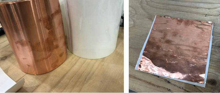
"LEFT: Two rolls: Copper Adhesive Foil Roll & White Vinyl. RIGHT: Copper on top of white material."
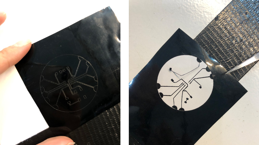
9B. CUTTING TIME
As I already used copper foil as a material for the assignment on week 3, I knew it needed a bit more of blade depth than usual. It worked pretty well.
"LEFT: Copper Foil right after using Roland machine to cut. RIGHT: First failed attempt to peel the circuit off."
Actually, the circuit that I failed to peel was damaged by the blade when cutting. The material had an imperfection and when the blade passed by it dragged some material damaging the trace.
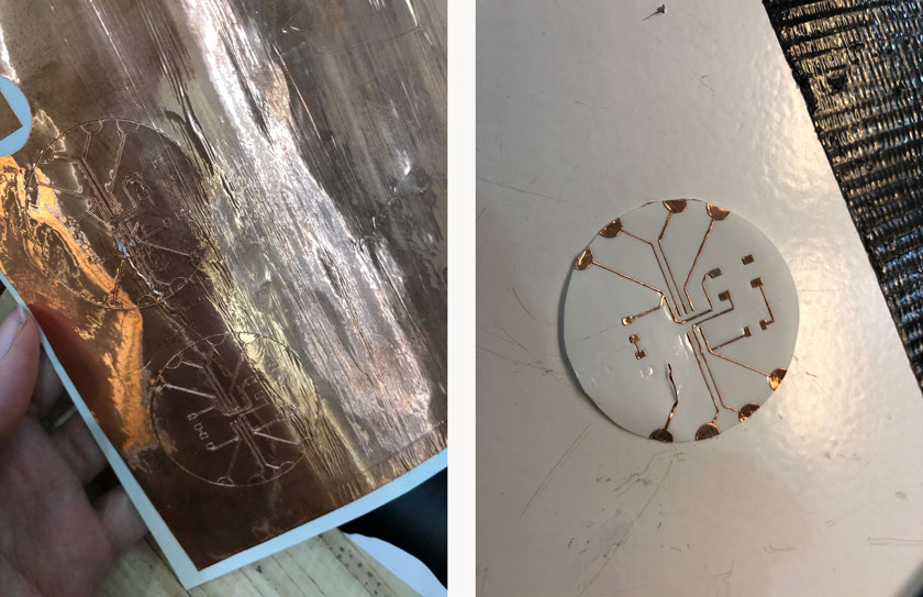
10B. PEELING THE COPPER
The adherence to the layer underneath the copper foil was pretty good. It was quite difficult to start peeling, but when you got the tip of the copper it was quite easy to be careful and remove it without damaging anything.
" Circuit after removing all excess copper ."
11B. SOLDERING TIME
Having soldered the slightly larger circuit before helped to go one notch down and solder this one uneventfully.
"LEFT: Soldered Copper Foil PCB. RIGHT: Holding the final PCB already trimmed and cleaned."
WHAT WENT WELL
Faster process: If you’re familiar with the pipeline this can be a very fast process
More reliable : Compared to the paper PCB this seems more durable and probably more reliable.
WHAT COULD BE BETTER
Delicate process:Compared to milling a PCB this
Some gaps: I still have some gaps to fully understand the usage of some features, mainly oscilloscope.
FINAL SHOT
All in all I’m pretty happy I was able to produce beautiful crafted ( even hand crafted) PCB’s for this week’s assignment.
"LEFT: Expand appearance job. RIGHT: Expand fill and stroke to make sure its all one object."
This results gives me some hints that I might want to keep exploring.
BONUS TRACK | PROGRAMMING ATTINY 45 USING ARDUINO ISP
Lastly, as I was very anxious to know if my paper circuit worked I tried to program it with Arduino. I will explaing the process in detail during the embbeded programming week, but in the meantime here goes a teaser:
All the programming process of the Attiny 45 boards (both hand made & laser cut) using Arduino ISP is explained step by step on week 8.
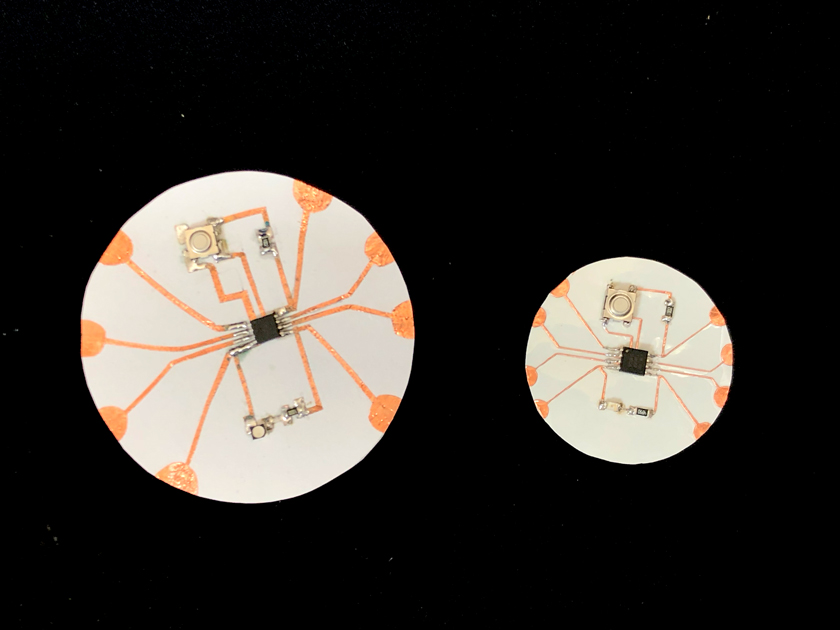
The setup developed this week was very rewarding as a flexible pcb. I also used it on Inputs Week to add a capative pompom which endup being super fun!
I really enjoyed working with the Attiny 45 and it ended up being my compagnion until the very end of my final project.
PUSHING THE ATTINY 45 WAY FURTHER - ATTINY 45 I2C MODULE
This is a small overview of what I achieved with this tiny friend. Go to the specific weeks linked here to see the full explanation for design & programming.
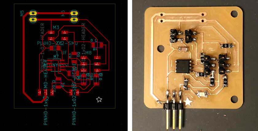
"LEFT: Kicad PCB with all components routed, ready to mill. RIGHT: Finished board number 1."
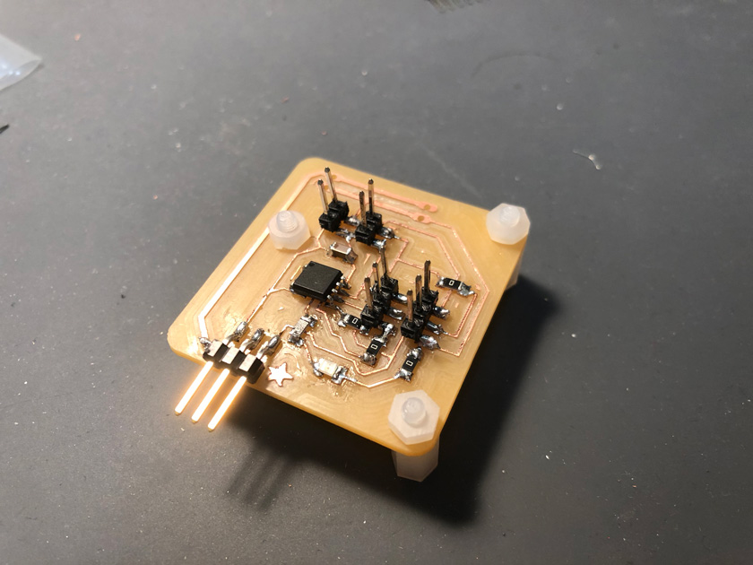
"Assembled secondary board 1"
Find all the info for the Attiny45 I2C board on week 13
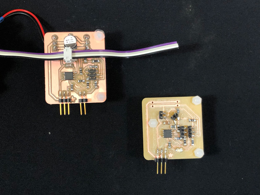
"2 iterations of the secondary board."
On week 16 you’ll find a second iteration of this same board that was more sturdy and almost ready to produce serially.