Electronics design 2.0
Group assignment
use the test equipment in your lab to observe the operation of a microcontroller circuit board
Here you can check the electronics design grop assignment
individual sssignment
Redraw an echo hello-world board, add (at least) a button and LED (with current-limiting resistor) check the design rules, make it, and test it extra credit: simulate its operation
individual assignment
As always this assignment is divided on several parts
- My 2020-2021 efforts
- Generalities on ECAD design
- TIPS AND TRICK ON EAGLE
- BOM
- conclusion
- Links and references
My 2020-2021 efforts
as i Stated in earlier assignments i started this journey to certification on 2020 and didn't met the requierements. then passed on 2021 and also didn't get to finish altough got to present my final projet.
So today in 2022 i've got to re write several of my original assignments.
HERE You can check what i did on 2020-2021 Electronics design assignement
Generalities on ECAD design
HERE on Mexico is not that common to find places to learn ECAD (electronical Computer aided design) altoguh it has similarities to conventional CAD it is completly diferent branch of design and workflow.
It is more common to find places were you can learn arduinos and conventional prototyping (using breadboards and simulators) than places were you can learn how to machine your own boards.
And to go even further, it's really dificult to find certain SMD components because all of the traditional fabrication methods use Trough hole technology (THT) because it has more room to error cause the components are bulkier and they're not so prone to make short circuit with out it has to be obvious.
Anywho....
Let's talk about the ECAD in general. I've tried a little bit of Fritzing, Altium and the original EAGLE.
Altough kicad is open-source really the standard on an industrial enviroment is EAGLE so i try to teach things that are more usefull on a real work enviroment.
Altough kiCAD is a piece of CAD i would like to really master some day.
Today i'm stuck with the conventional licensed and boring ECAD.
On 2020 i started my designs on Autodesk's EAGLE.
In that time you could download a Stand alone version of the software using the educative account on autodesk's page.
during 2020 outbreak had "technical dificulties" with my laptop. So had to reinstall eagle on a new laptop
then i realized that it is not possible to install only eagle anymore.
i do not know who was the genious behind that idea.
but now you have to install a mechanical CAD/CAE tool to have eagle.
it's like having 3 softwares installed all at once.
it's heavier to run on a regular laptop altough it's cheaper on a long run just to pay for 1 license than to pay 3.

Fusion 360 it's the new enviroment for CAD on eagle
Anyway, after you finish the installation. open up Fusion 360 you'll have to go to file/open electrical design in order to get to the forst step of eagle wich is open up a project or create a new one.
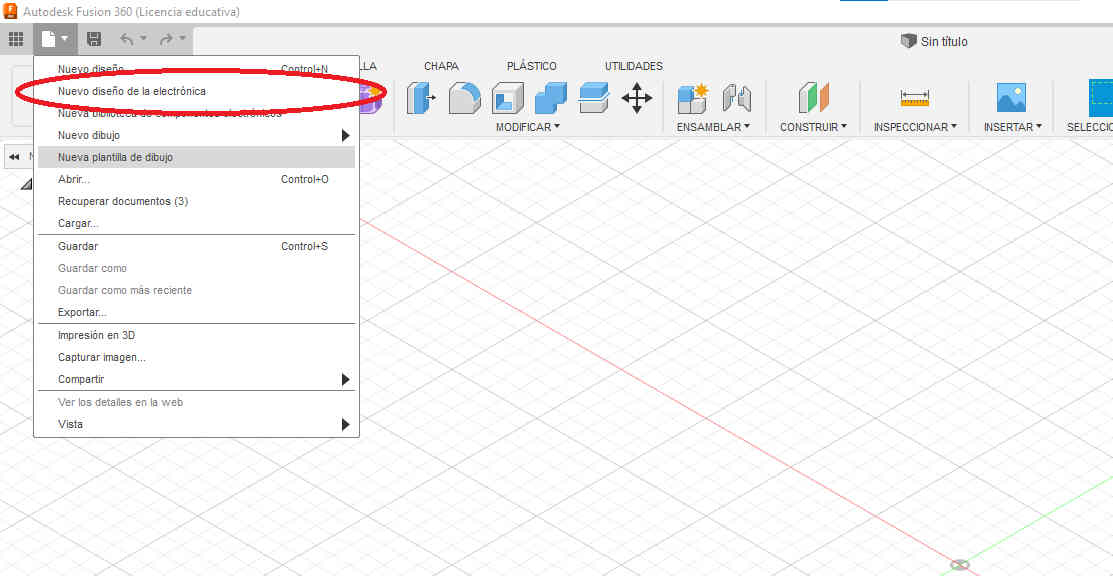
Whats a project?
it's an special type of file that's the link or bond between 2 diferent types of files in eagle the scheme (*sch) and board (*brd) files. Each one has it's own workflow whitin. Altough you can do really complex things like PC motherboards with multilayer boards, gnd and noise shielding. i only know how to engrave the first layer.
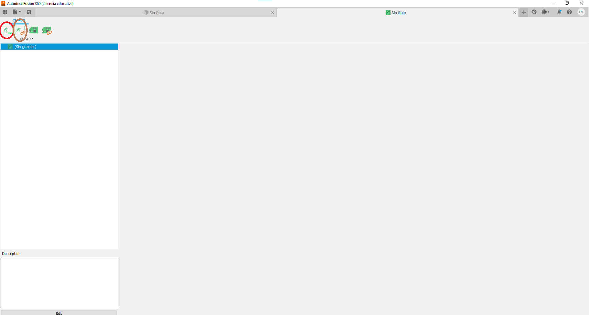
create a new scheme (red circle) link an existing (brown circle) for when you're downloading schemes from other person and you get the "no relation between sch and brd" error.
beacuse of my mechanical design background i'm gonna make this analogy frecuently.
in a SCH the polylines are called nets and the can be in two diferent types explicit or implicit (visible or invisible) they set logical conections between components.
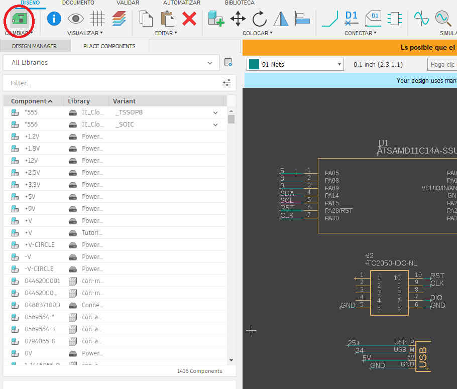
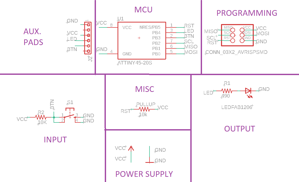
i based my design on adrian torres samdino because i want to used this board to input devices, output devices networking & comm and interface and appilications.
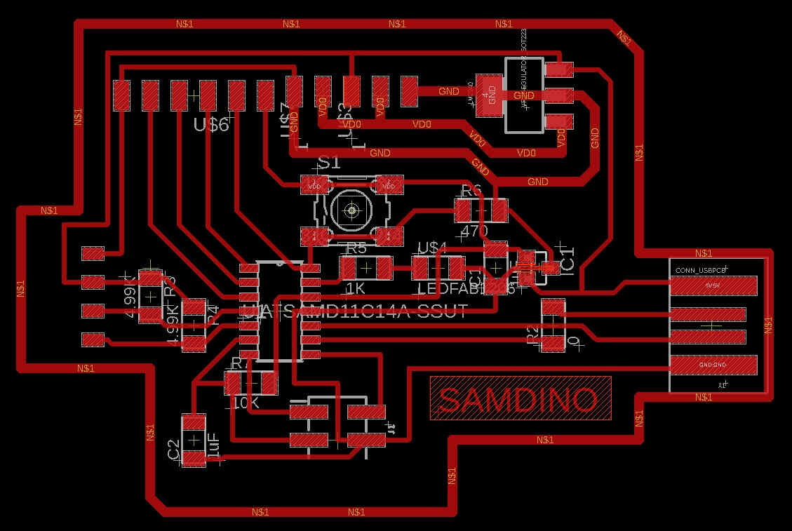
adrian's samdino
al tough i generaly speaking i think he did a great job i modify it a little bit to make it a little clearer
First he has a gnd trace in between 5vdc and 3.3 vdc on the lineal voltage regulator that's to tight not for the cnc but for my soldering skills. so y placed a 0 ohm resistor to be a jumper just to make sure the regulator does not have a solder bridge.
then adrian has smd jumper wire female conectors and and for me that's usually a big no no in design because the cooper pads are just to fragile to make them take mechanical stress of conecting and disconecting things.
Also i removed the voltage regulator to feed with a 9V battery.
and placed extras 5v and 3.3v vcc as well as gnd.
the general workflow on the SCH files it's kinda like this.
- Open a new Scheme
- Place components
- set nets
- set names and/or values to the nets and components
- go to create the board file
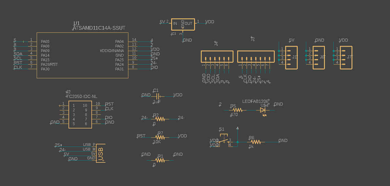
this is my SCH file
HERE you can download my EAGLE FILES
in the button shaped like a pcb board you can change the view to board file (ctrl+2)
in the BRD files the nets becomes airwires (it makes nosense to me but however.)
then the general workflow on a BRD file i't like this.
- Edit the DRC (design rules check)
- Place all of the components inside the default pcb dimension.
- orient all of the components in a way that makes sense.
- Draw all of the essential airwires manually
- then auto route the rest of the airwires.
- try to make sense out of even the lines(they have to be clear to see were they conect and how they conect.)
neil only talks about SMD components but as i said before it's really dificult for me to get all of the required components in time from an international vendor like digikey. it's easier to go to the local electronic store and get 50 THT 1Kohm resistors than to wait 2 weeks to get them in SMD version from digi-key.
So it's logical to simply draw components that are THT or SMD depending on what i have in stock in the inventory on the fablab.
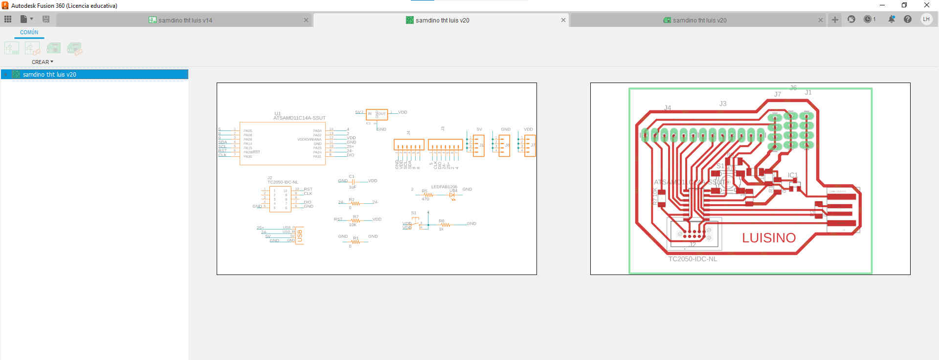
this is what the project file should look like when you're working between two files sch (ctrl+1) and brd (ctrl+2).
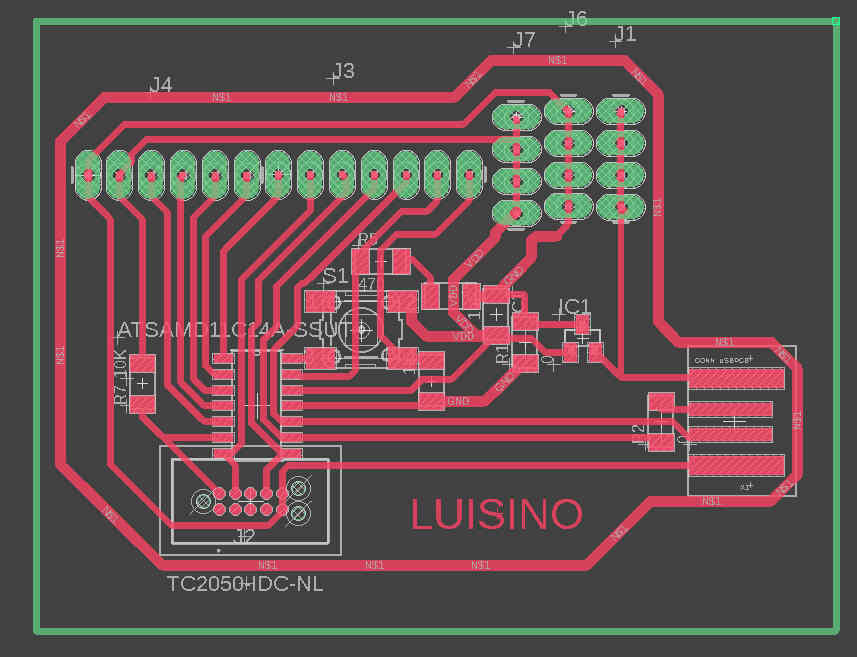
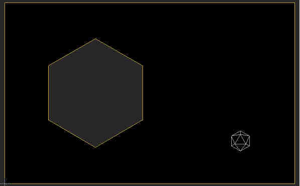
this is a screenshot on the board file of my version of the samdino.
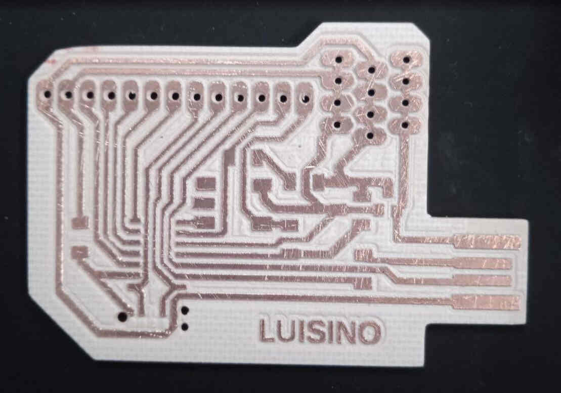
this is the board out of the cnc ready to get stuffed
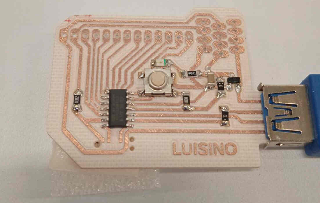
this is a picture of the board already stuffed
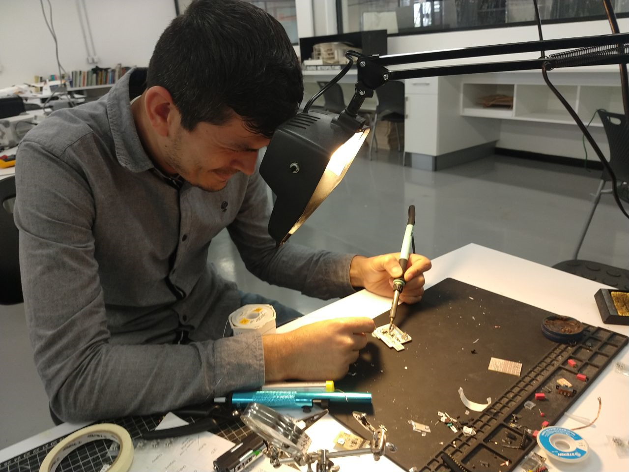
this is a pic on the soldering process.
TIPS AND TRICKS ON EAGLE
you have two choices to create your conections between components
you can create lines using comand net like in the picture above
Or you can create what eagle calls "implicit" lines using name in the command line and clicking on the line you want to conect.
to create an "implicit" conection you just have to give the same names to the lines you want to conect on the board file.
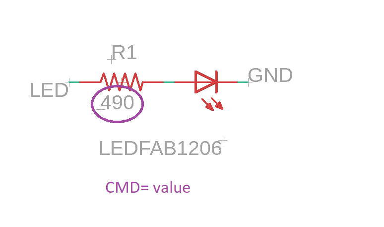
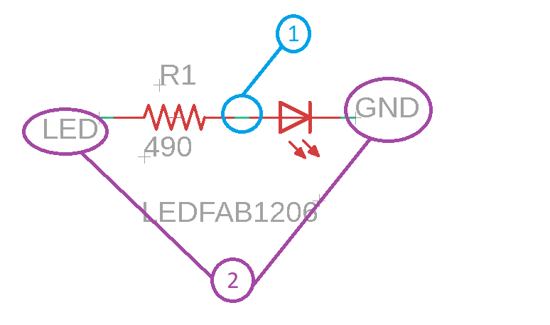
you can also give values to certain elements like resistors capaciors
you just need to type value on the command line and click on the component.
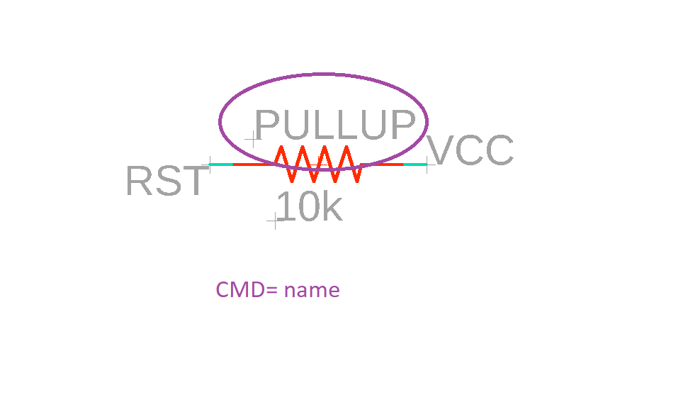
you can give names to components like the pullup resistor i used to the rst pin on the MCU like in the picture above
both of the components of the picture below serves the same function but the one that states "right component" at the bottom of the pic is easier to solder.
always search components that suits you necesities.
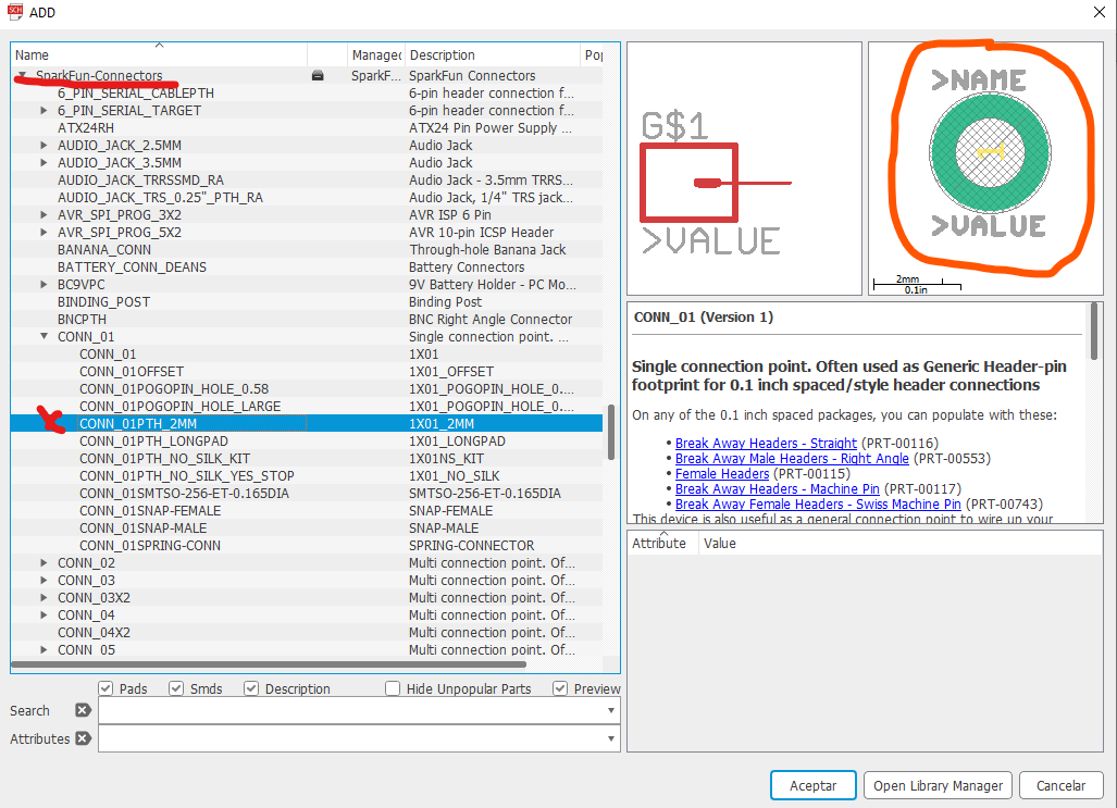
wrong component
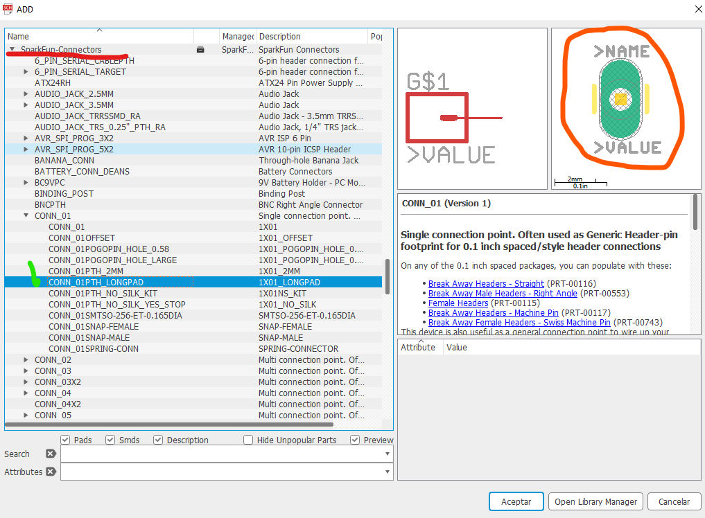
right component
EAGLE already has a lot of compoents to choose aditionally you could use the FABcomponents or download a new individual component from a web page
i personally recomend component search engine.com because it gives you libraries for kikad, eagle and fritzing.
but there are a lot of usefull component libraries in the library manager on eagle go to:
add part button/open library manager button/available tab/and add whatever you find interesting licking in the "use" button
it's better to keep well organized your diagrams in case you need to redesign something.
or some one else is trying to use the file as an example.
I try to use this system in all of my eagle projects.
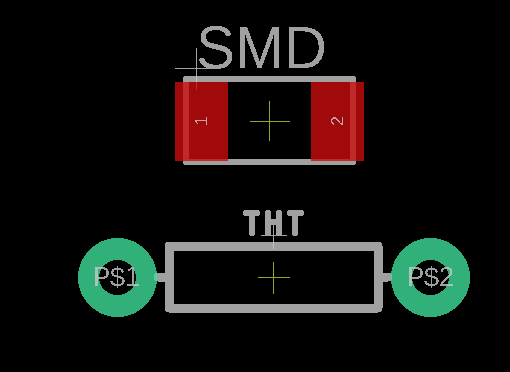
RED pads mean smd component and green ones means a through hole components
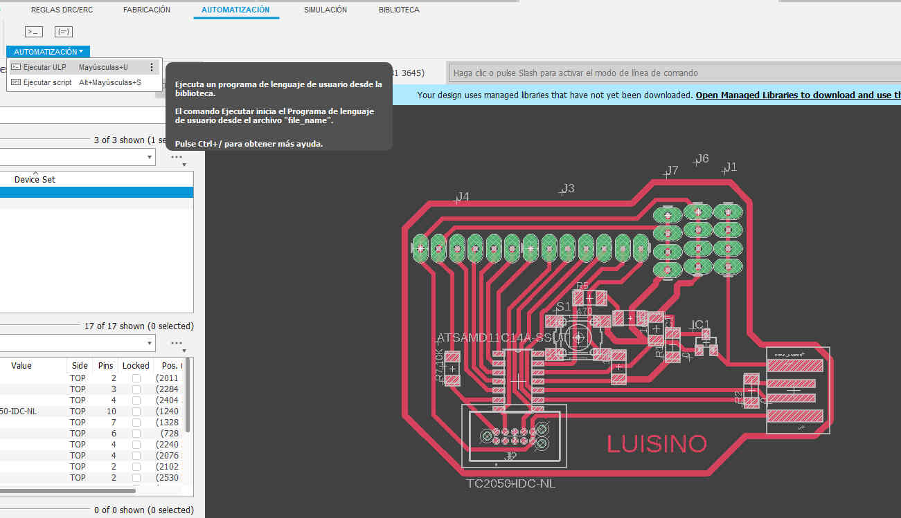
for importing dxf into eagle go to automatization/run ULP
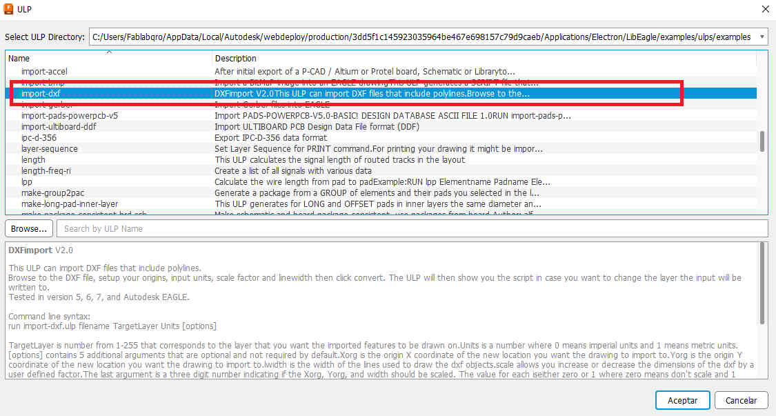
run import-dxf
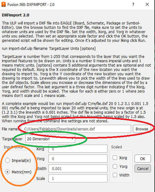
select the file (green),choose a layer to import (green) usually dimension and then check the units of the dxf (orange) usually millimeters
right click on any line then propierties and you can change the width of only that selected line segment
i recomend to edit the DRC (design rules check) at the begining to avoid futures pain in the neck every time you open your board for the first time
type drc oin the command line to open the window like in the picture below.
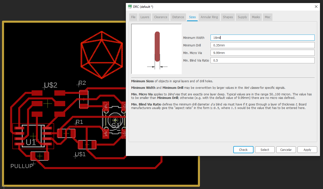
the wider the line you made the easier is to solder. but also the wider the bigger the noise you get in your circuit (basically works like an antena).
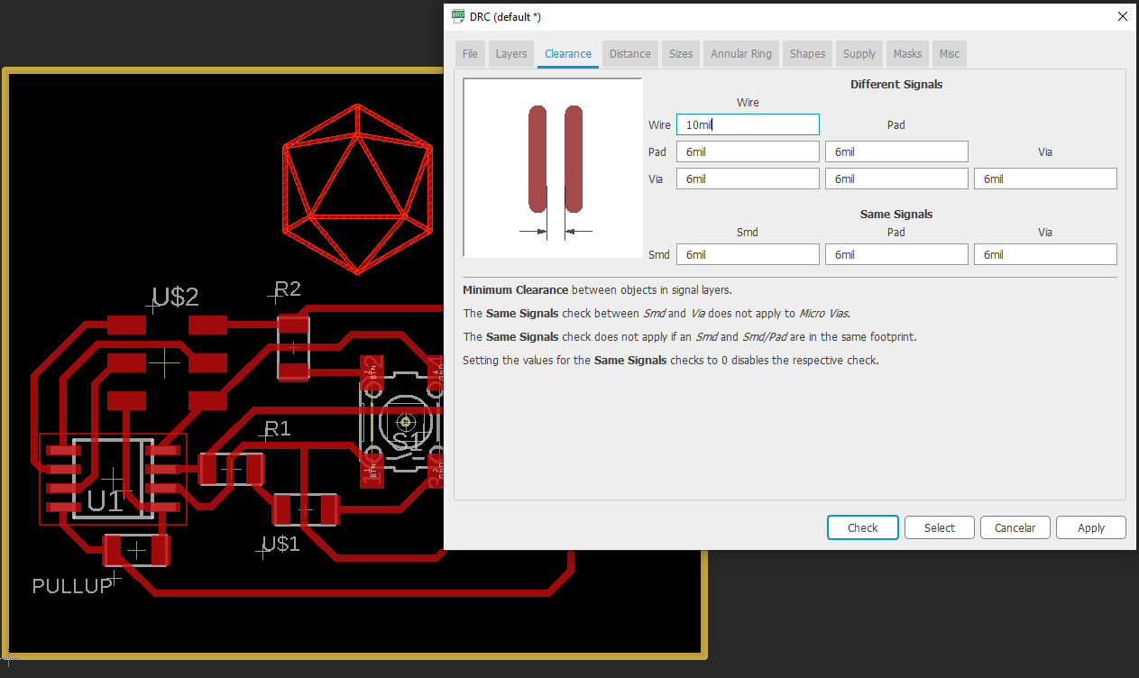
choose a minimum clearance between routes that fits your machine capabilities. (i choose 10 mil for this brd)
Also if you have no idea of what you were doing like me. you can set the autorouter function to do all of the copper wires for you.
click on the auto router button on the right side of the screen.
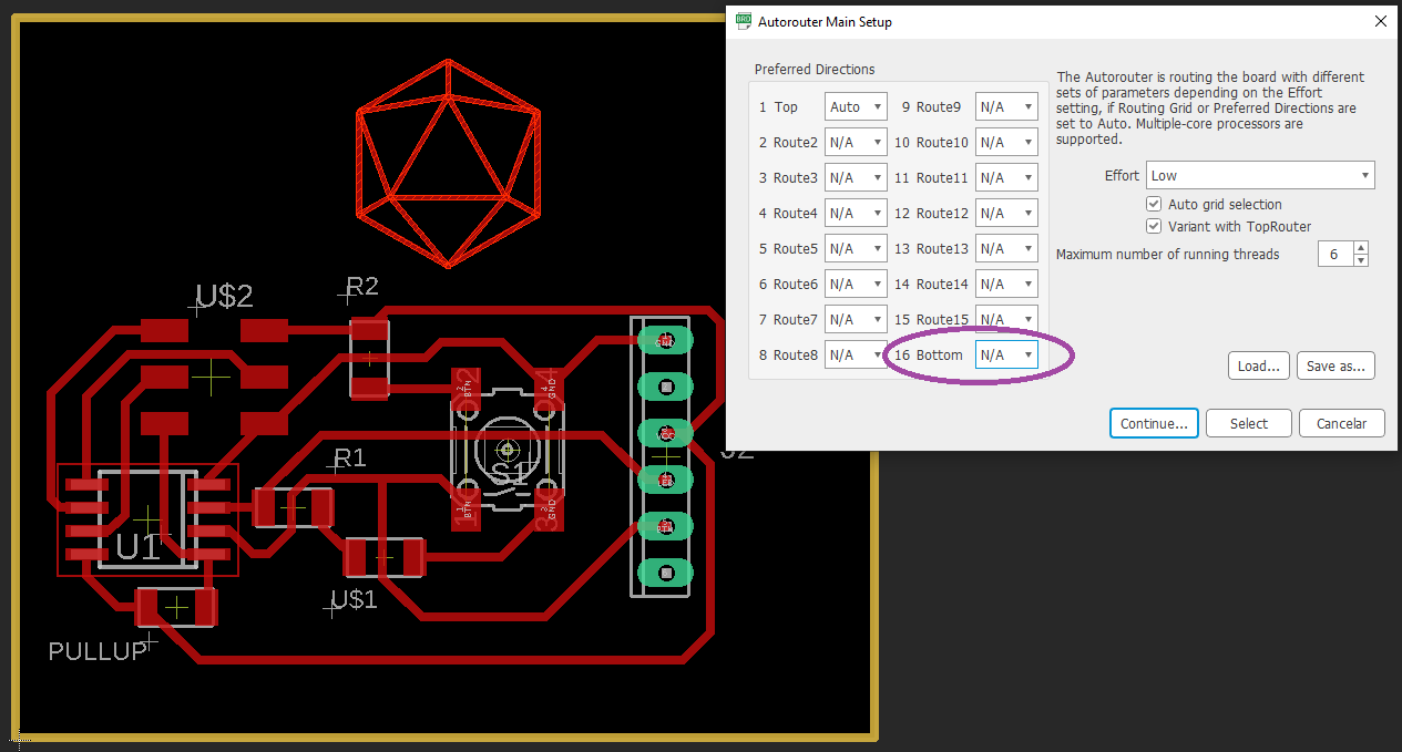
remember to set te bottom layer to N/A like in the picture above. Otherwise you'll end doing a double sided pcb on the auto router function
BOM
- (1) SAMD11C14
- (1) 1 uF Ceramic Capacitor
- (2) 0 ohm Resistor (jumper)
- (1) pulse button
- (1) SMD LED
- (1) 499 ohm SMD resistor
- (1) 1 Kohm SMD resistor
- (1) 10 Kohm SMD resistor
- (1) 3.3 linear voltage regulator
- (25) THT jumper cable male conector
conclusion
in this assignment there's a lot involved.
you can not start designing something from scratch if you don't know which pin does what.
and you can't know wich pin to conect to what if you don´t have a basic knowledge of electronics and know how to give a pull up value, how to transform 5v into 3.3v, how a diode works,etc.
all of this topics shoud be covered by the instructor before the assignment take place so i understood what to do.
one should use 45° angles in traces preferebly over 90° angles in any board. (i've found 90° angles are very fragile and rip up from the sustrate way easier).
i've also used Vcarve to generate the CAM files
links and references
Roland SRM-20 file
Vcarve pro 9.0 file
Component Search Engine
Eagle files
Generic Standard on Printed Board Design
basics on how to properly route a pcb on eagle