Electronics design
Update 06/07/21
Group assignment
use the test equipment in your lab to observe the operation of a microcontroller circuit board
Here you can check the electronics design grop assignment
individual sssignment
individual sssignment
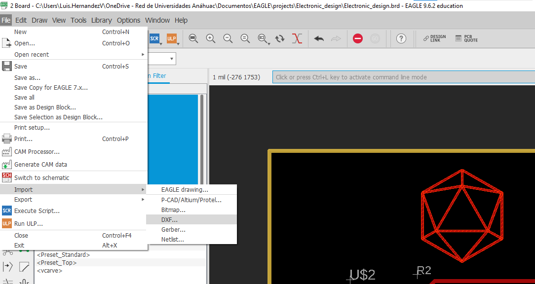
for this assignemnt i used autodesk's eagle software here you can download an educative version you only have to create an educative account to redraw an echo-hello-world board based on the ATTiny44a chip here you can see the board i based my design once installed and decided which board to start from the process is pretty straight forward create a project that contains a scheme and a board file.
first i downloaded the libriaries following the instructive my instructor gave us.
- 1.- first download the files and unzip them from this link eagle libraries
- 2.- then copy the file in my case was C:\Users\Luis.HernandezV\Documents\EAGLE\libraries
- 3.- Then restart eagle in case you already had it open
now it's time to place all the components and their respective conections so the software know what pad conect with wich pad
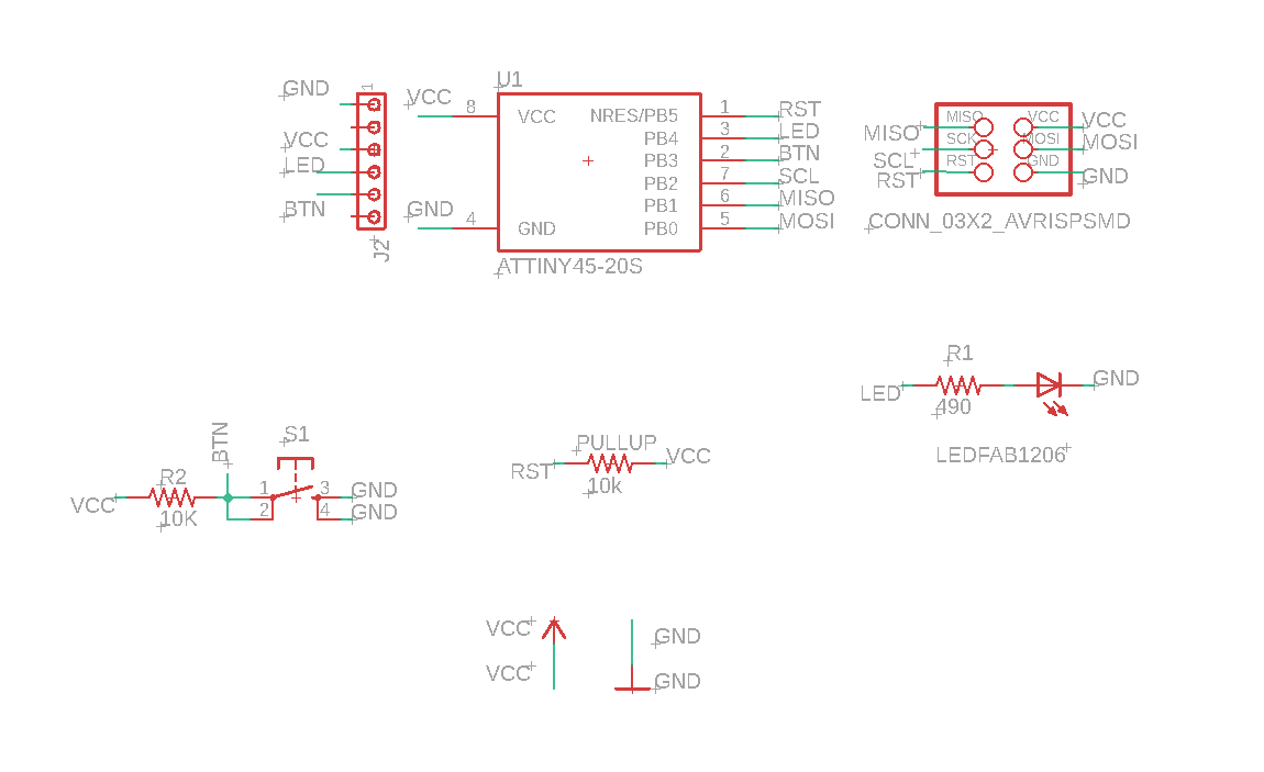
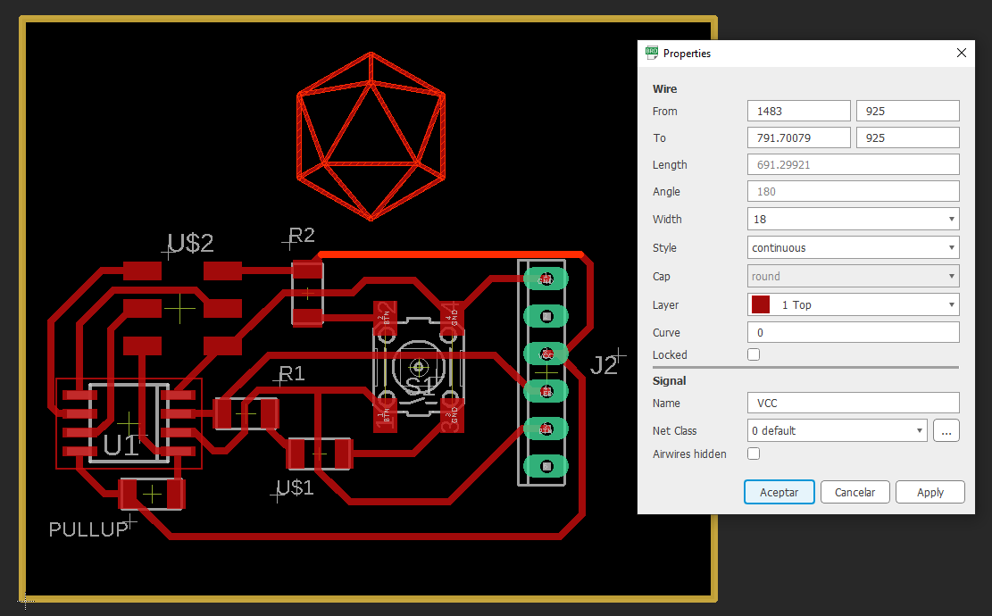
 this is my final scheme
Now i clicked on the button to generate the board from the schematic file
this is the version that really made the final cut.
TIPS AND TRICKS
you have two choices to create your conections between components
you can create lines using comand net like in the picture above
Or you can create what eagle calls "implicit" lines using name in the command line and clicking on the line you want to conect.
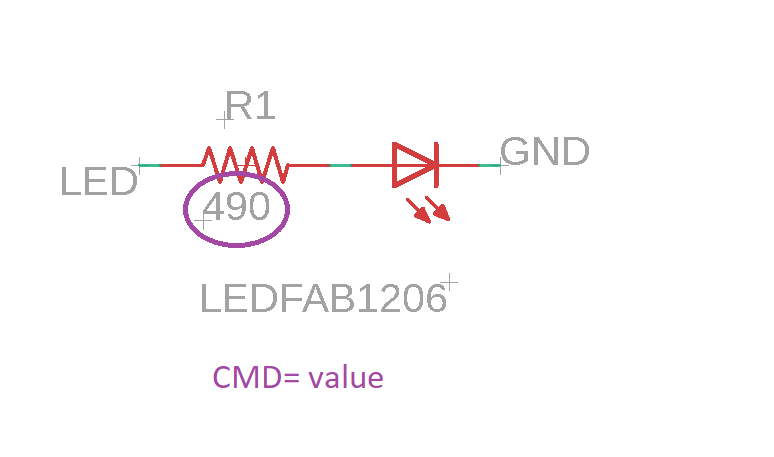
you can also give values to certain elements like resistors capaciors
you just need to type value on the command line and click on the component.
always search components that suits you necesities.
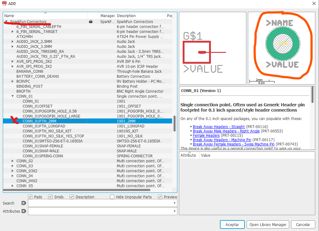
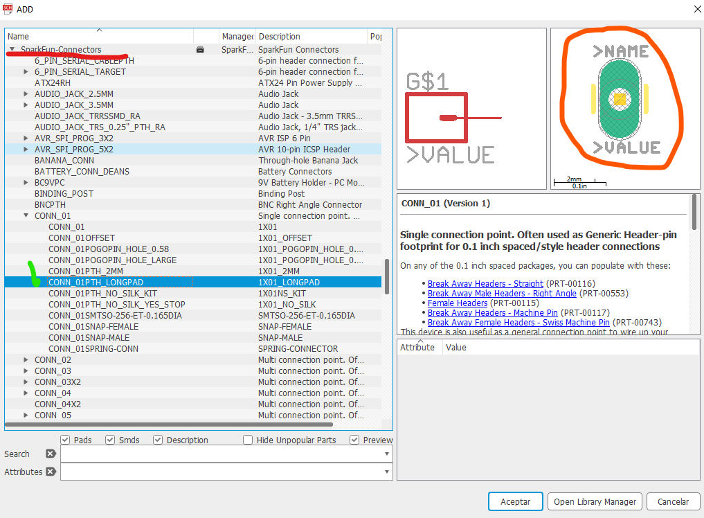
but there are a lot of usefull component libraries in the library manager on eagle go to:
it's better to keep well organized your diagrams in case you need to redesign something.
or some one else is trying to use the file as an example.
I try to use this system in all of my eagle projects.
when you are ready click the "Generate/switch to board" button to create the brd file.
this yellow lines are guides to show you where correspond in your sch file.
you have to create "routes" in order place copper in the pcb.
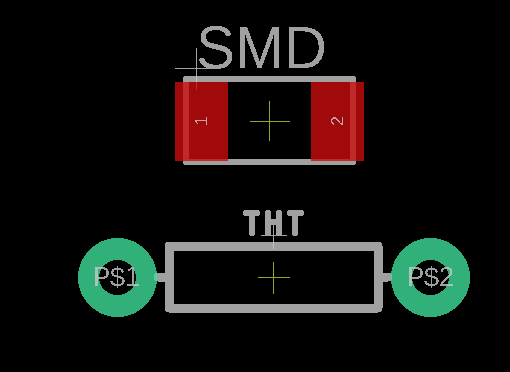
RED pads mean smd component and green ones means a through hole components
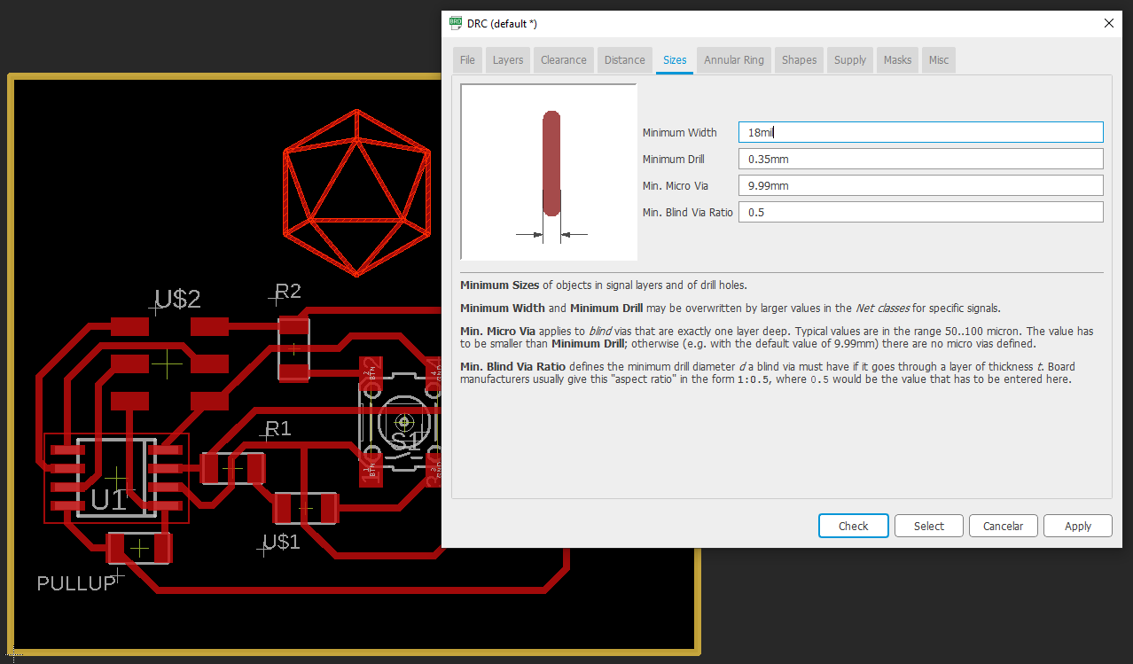
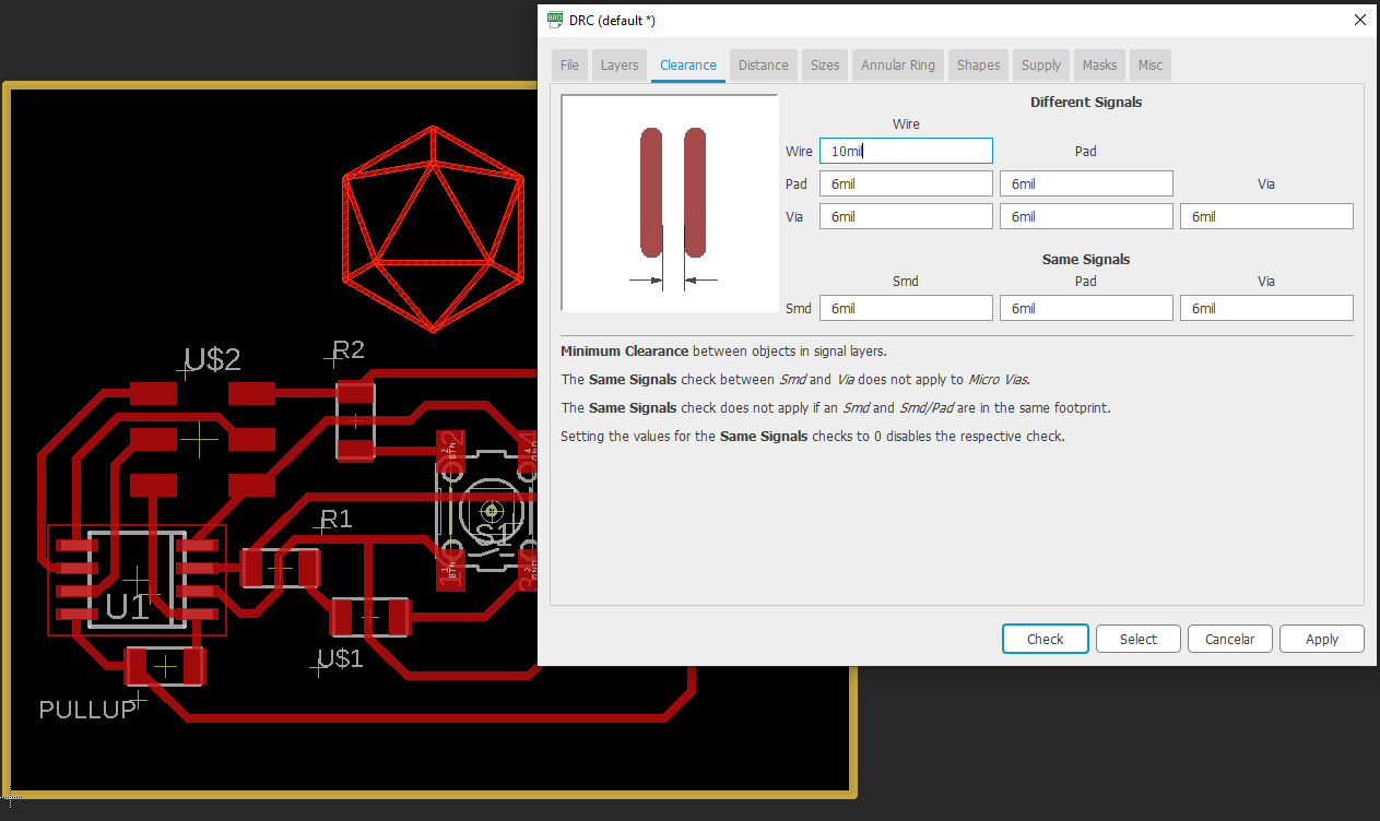
type drc oin the command line to open the window like in the picture below.
click on the auto router button on the right side of the screen.
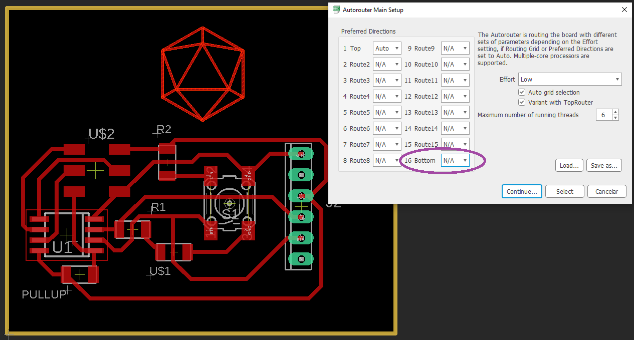
remember to set te bottom layer to N/A like in the picture above. Otherwise you'll end doing a double sided pcb.
then leave the autorouter set the routes to ground and voltage.
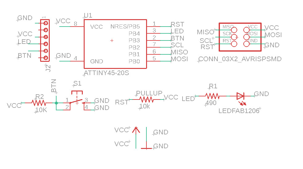
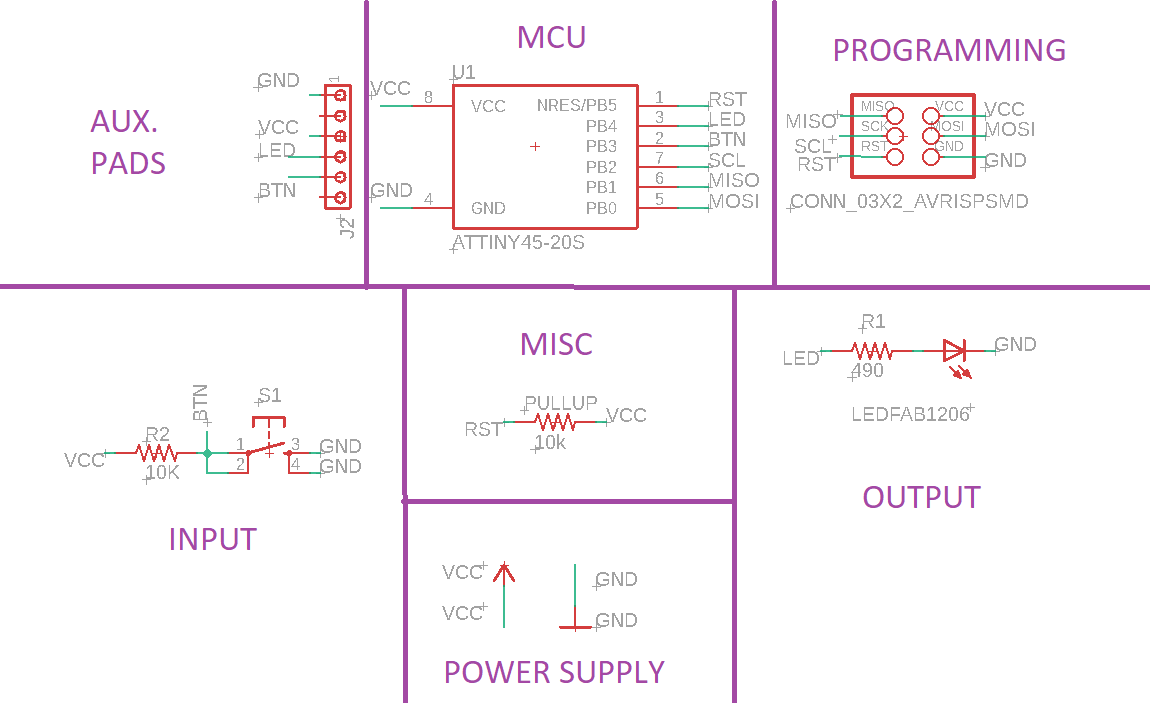
schematic on the echoboard using t45
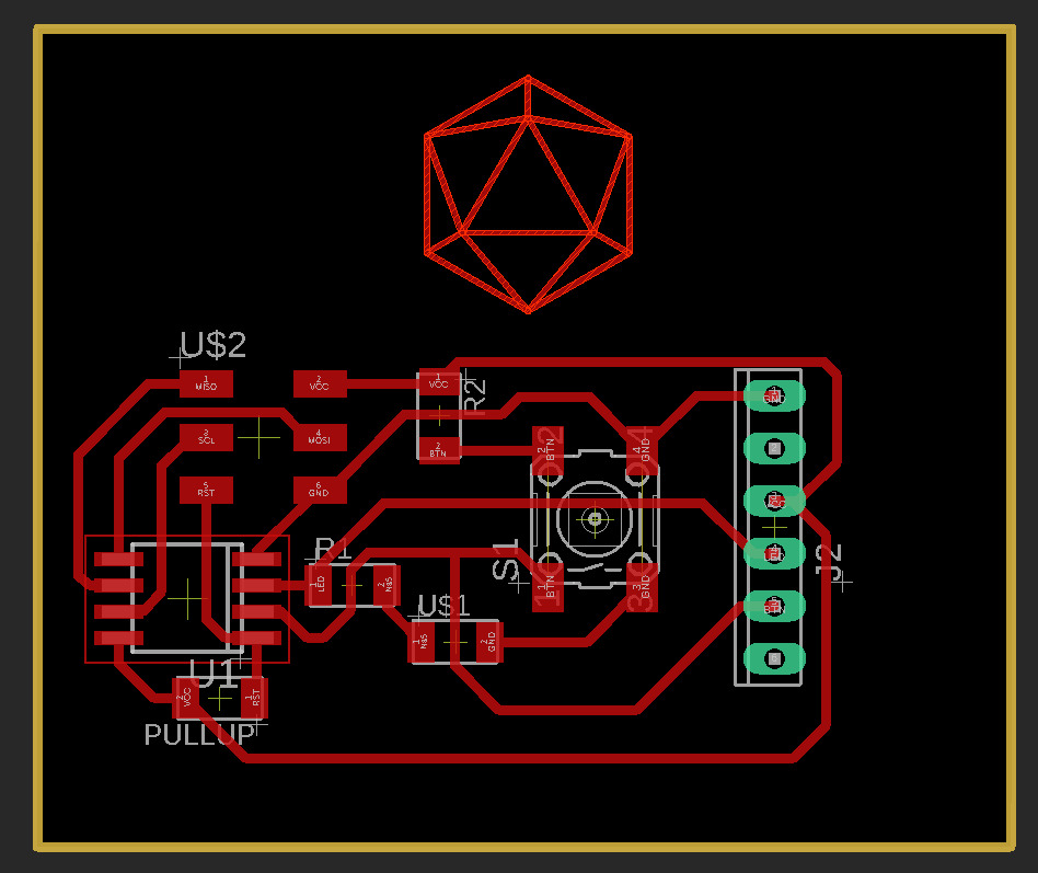
board on the echoboard using t45
HERE you can download all of the files for this board (Vcarve,roland srm20- gcode ,sch & brd for eagle)
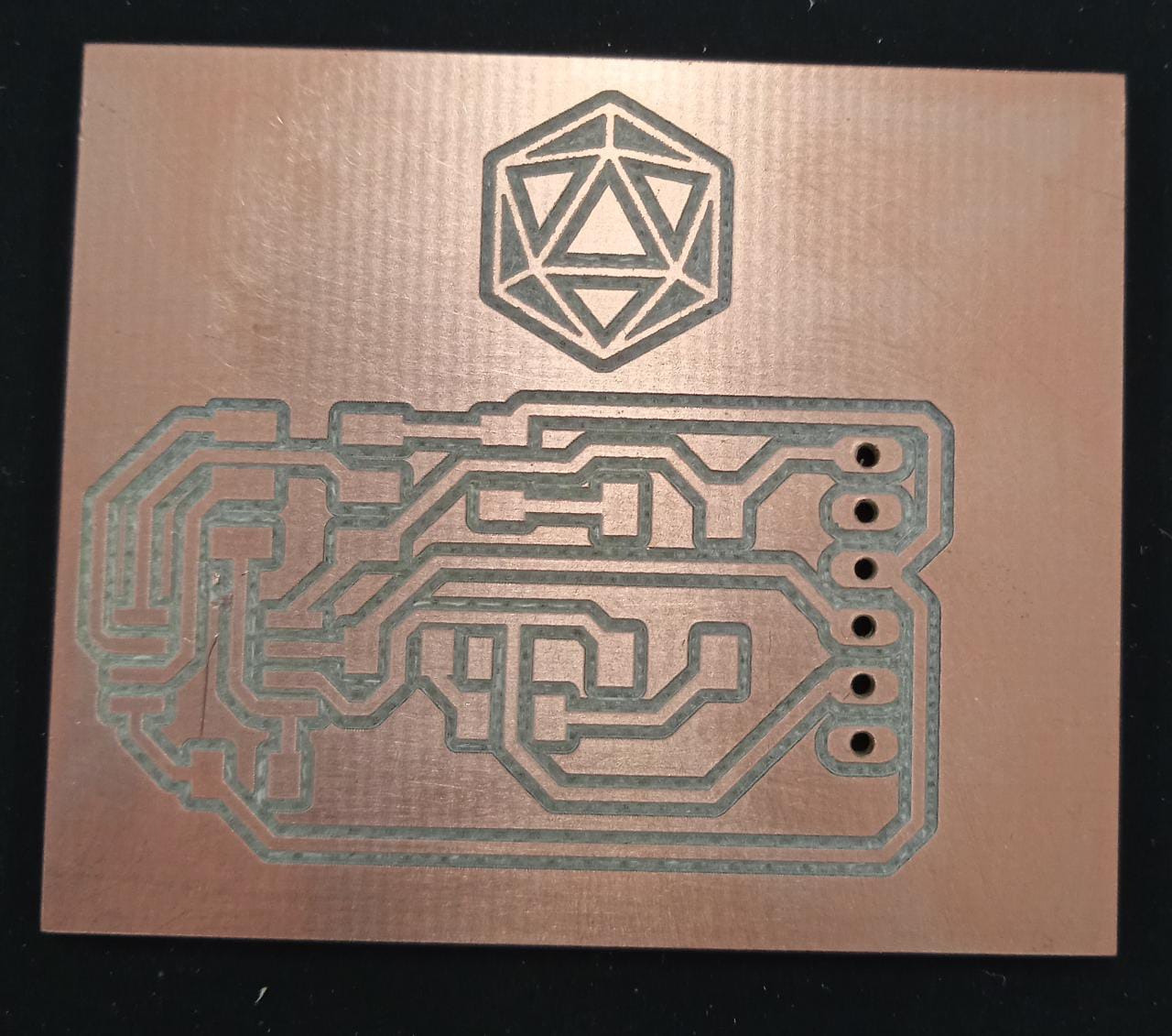
after milling and cutting it. Finally it was time to solder it so i'm going to list here the bill of materials
bill of materials
- 1.- (1) ATTiny45
- 2.- (1) Tactile switch
- 3.- (1) 2X3 header
- 4.- (1) 1X6 Header
- 5.- (1) SMD LED green clear
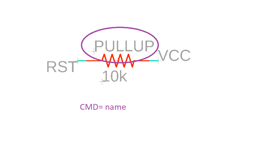
- 6.- (2) resistor 10k ohm (one pullup for the button and one for the reset)
- 7.- (1) resistor 499 ohm (for the LED)
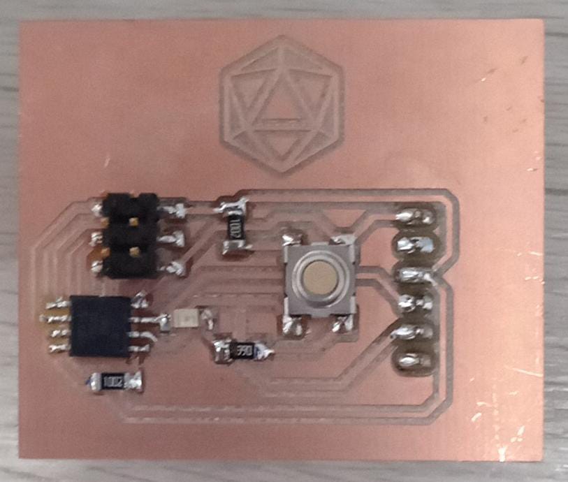
after soldering all was time to program it
here i will post what i updated on this assignment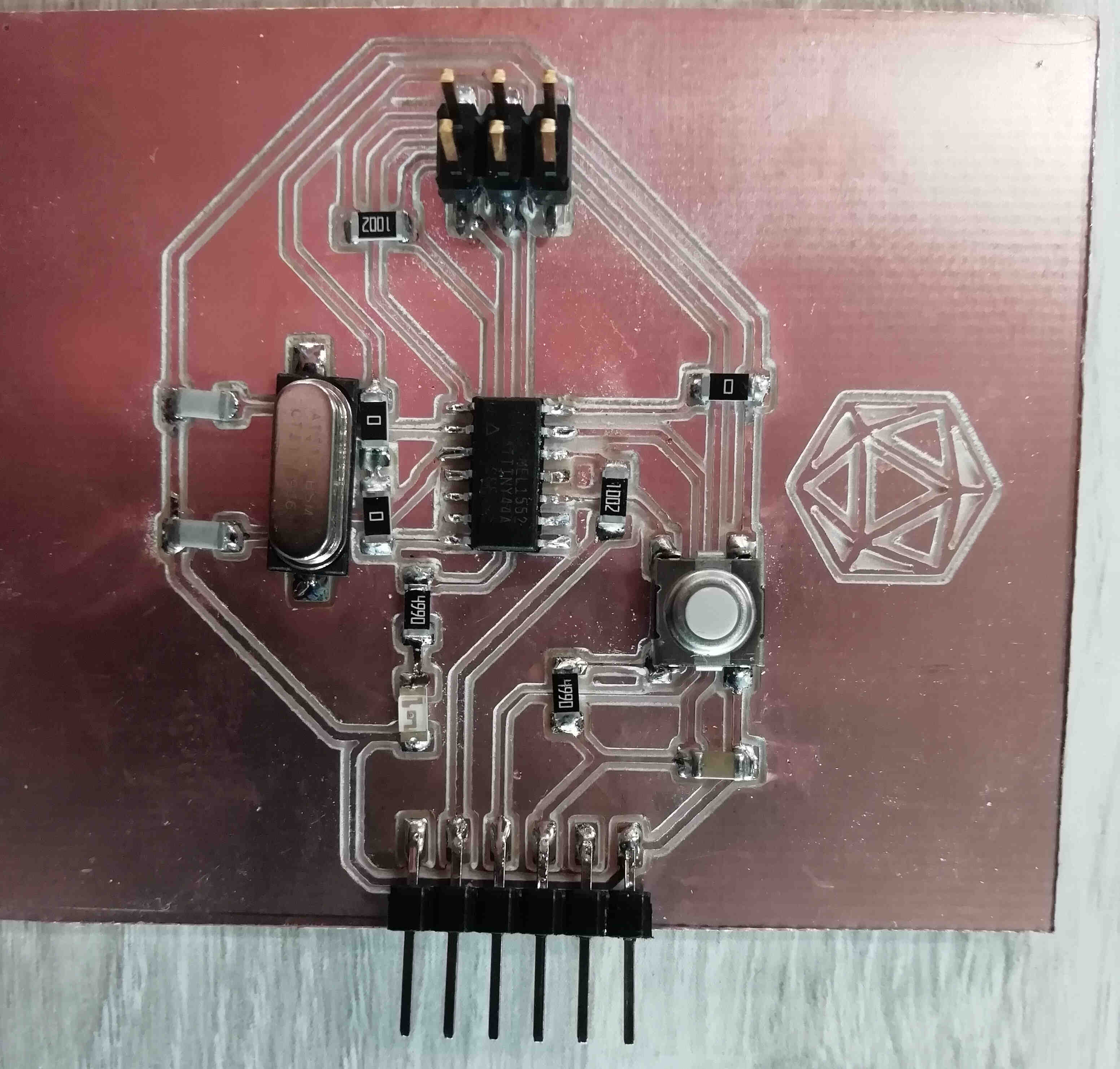 picture of the echo dragon V1
this is the work i did during COVID-19 quarantine.
and this is the echodragon v3
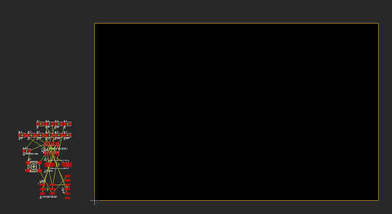
a screenshot on the schematic file of the echodragon v3
a screenshot on the board file of the echodragon v3
a picture of the pcb completily finishied
this is a video of the whole process
picture of the echo dragon V1
this is the work i did during COVID-19 quarantine.
and this is the echodragon v3
a screenshot on the schematic file of the echodragon v3
a screenshot on the board file of the echodragon v3
a picture of the pcb completily finishied
this is a video of the whole process
- the process of the toolpath generation (i give a lot of detail into electronics production week)
- the soldering process (althoug a little boring i'm very proud of this little achivement)
- uploading a blink sketch using a dev kit though.
- testing the sketch i've made using the arduino IDE
please be gentle it involved a lot of effort for my self to edit the video on premiere pro.
i repeated this sketch in embedded programming week using an ISP
this is a video of the fabrication including testing it with a blinkthis is the text on the ino file.
this is a video of me testing the button sketchobviously i had to compress it in order to push it to my repo but i will host it in here if you like to see it in detail.
links and references
here you can download the fabrication files of the PCB
here you can download the sketch for arduino to control the board
HERE This is the tutorial that teached me how to control a LED
WSL (windows subsystem for linux
2018 jimena's embedded programming week
2016 vinod's embedded programming week
2016 JC CHANG's embedded programming week
youtube tutorials i followed
how to install AVR drivers on windows 10