7. Electronics Design
1. Individual assignment; Redesigning Hello Word -board
To Redesign the boards first the schematics were obtained.
To This board an LED and a button are added. LED needs also a current limiting resistor. The button needs a couple of passive components for debounce circuitry.
For the PCB design Autodesk Eagle was used.
Before anything can be done. The FabLibary needs to be installed.
.png)
.png)
.png)
The libraries were then added to Eagle.
.png)
.png)
.png)
.png)
Schematic
A new project was created and opened. From the File>New>Project.
.png)
.png)
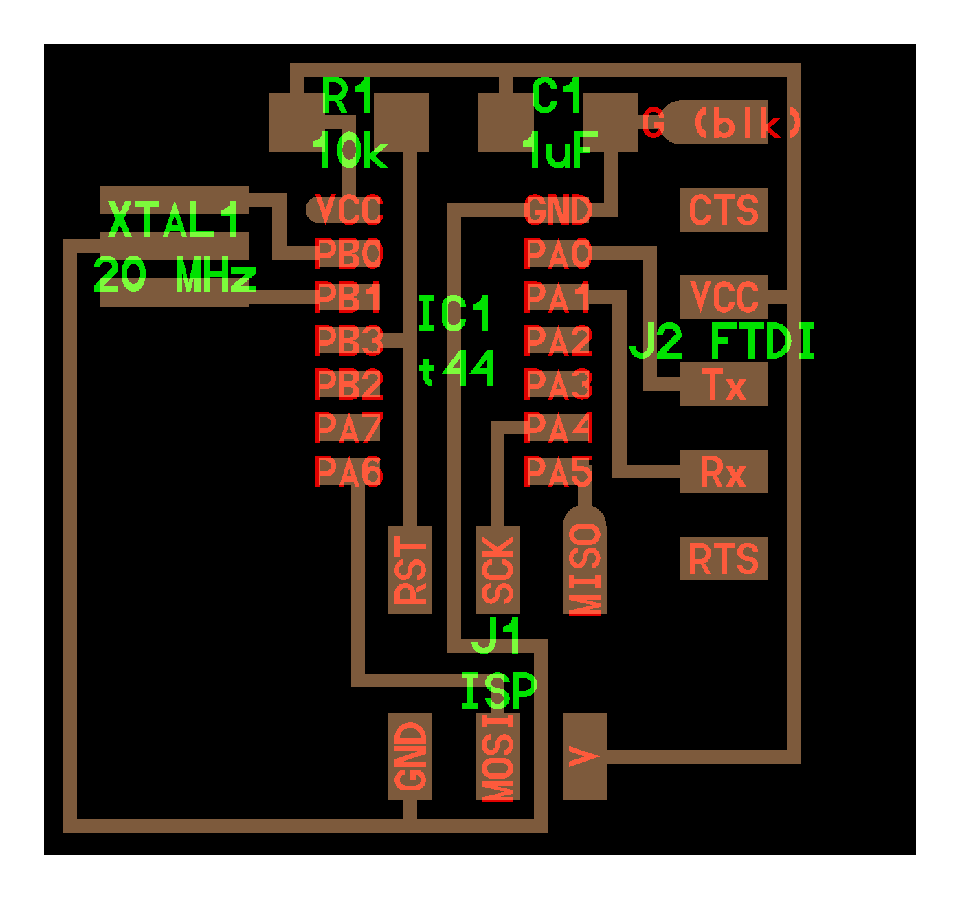
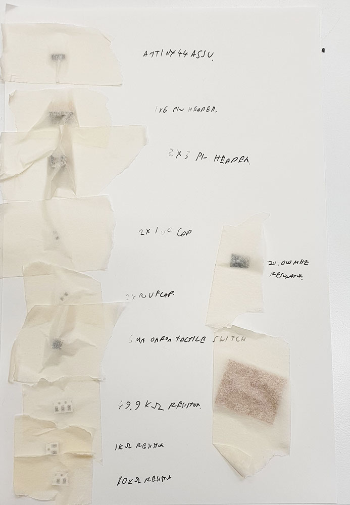
Needed parts:
- ATTINY44-SSU
- 20MHz Resonator
- AVRISPSMD 2x3-pin connector header.
- 1x6-pin smd side connector.
- 1x 10k ohm resistor Pull up resistor for header vcc.
- 2x 49.9k ohm resistor. Debounce voltage ladder
- 1x Omron 6mm Button The Button
- 1x 1 uF Capacitor Debounce filter
- 1x 10 uF Capacitor attiny44a Vcc filtering
- 1x 1k ohm resistor Red LED current restrict.
- Red LED The extra part
The parts were them randomly added to the schematics.
.png)
.png)
.png)
.png)
.png)
.png)
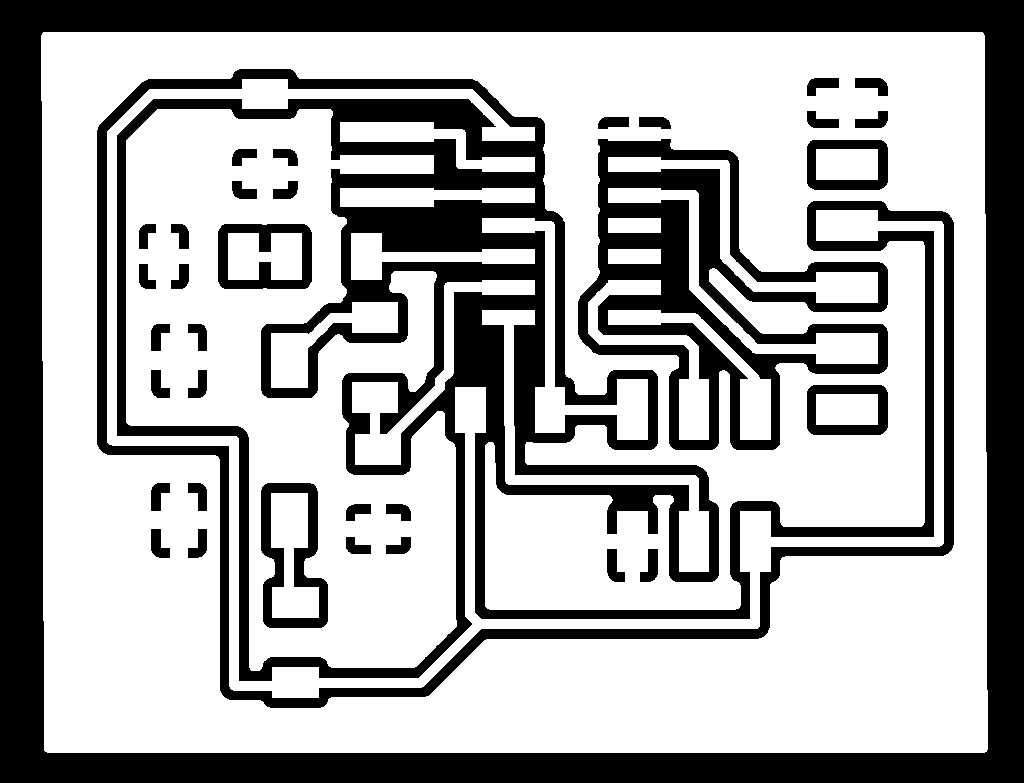
The components need to be moved on the design space and placed so that the connections can be made without interference or crossings.
The Design rules was firs adjusted for the machine on the fablab. The diameter for the milling bit is 16mil
.png)
.png)
After the design parameters were adjusted the design itself can begin.
The autorouter design tool was tried with interesting results.
.png)
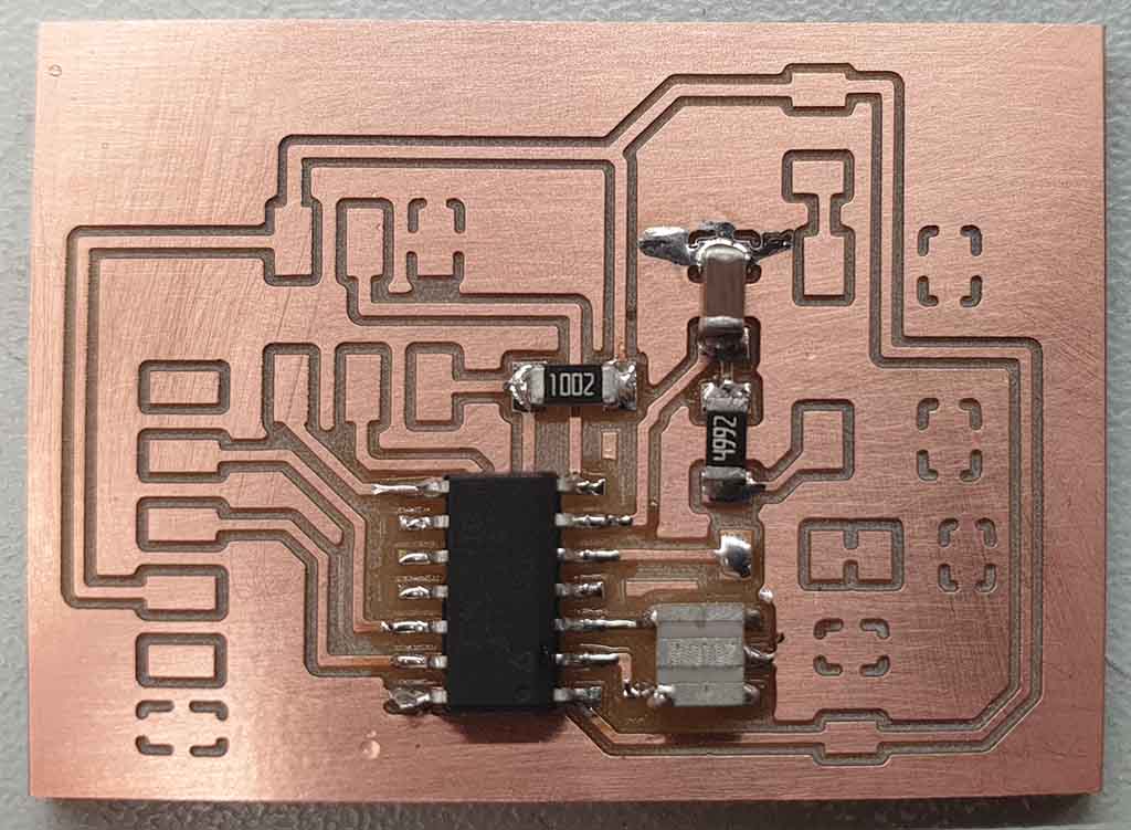
The traces were then designed by hand.
.png)
Few words about the design.ATTiny input capasitator was also used as the resonator ground dampener by placing the capasitator ground near the resonator ground connection. The button also doubles as a jumper to the GND to jump over the 5V trace pull around the board.
After the traces was made the ground plane is nested around everyhing.
.png)
After The Ratsnest button is pushed.
This creates a ground plane that connect every GND tab. This also reduces the milling time because more copper is left on the board. Also the copper ground plane conducts more current,shields from EMP disturbance and cools hotspots by heat conduction.
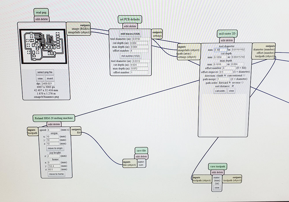
The Design was then exported to milling.
.png)
.png)
The expoting to PNG milling.
.png)
.png)
.png)
.png)
The straight export from Eagle produced a png image of 3x size of the intended 4007x3063pix at 12021x9189pix. One reason can be the used 4K resolution monitor. But the scaling is a tad odd. The nominal 1080P would be 1/4th scaling, not 1/3. Nevertheless, I first tried to upload to mods and set the resolution of the input png to 12021x9189pix. Pressing the calculate button promptly crashed the site. The crash was so hard that the site crashed apparently from everybody. Three people from three different computers working in the same room trying to make the traces for the milling reported that the site did not load anymore. The site was again reached after 20 minutes of waiting. After this the image was scaled down in Gimp to required 4007x3063pix. After this the calculation finished normally

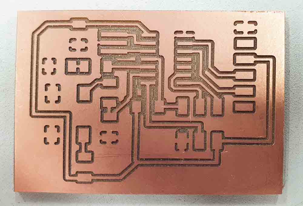
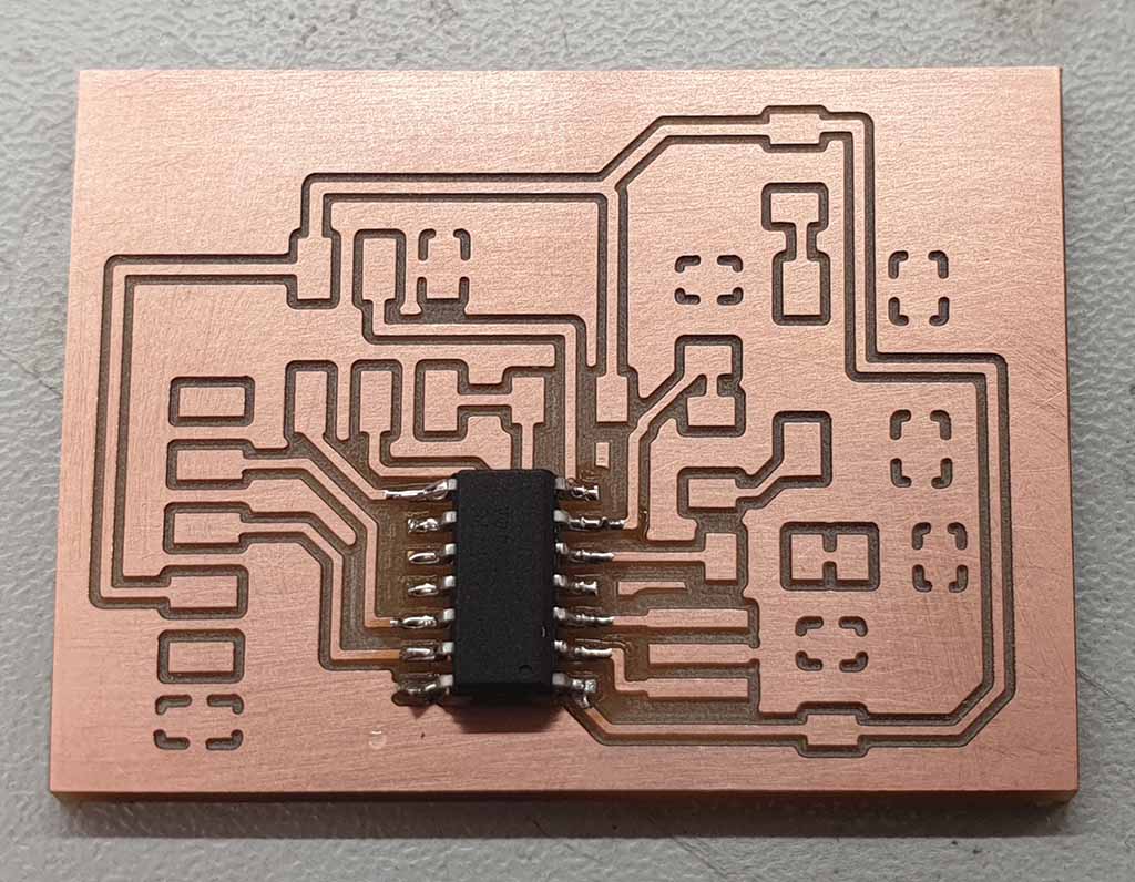
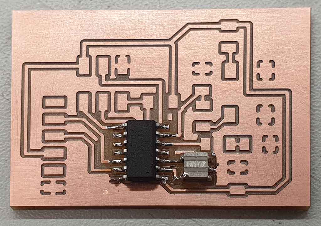
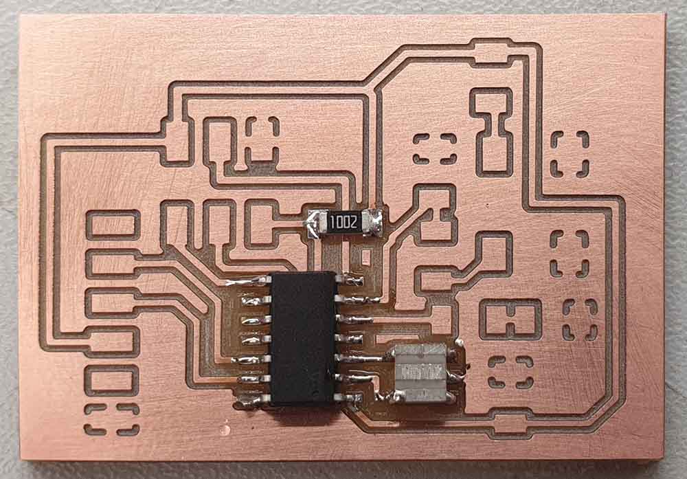
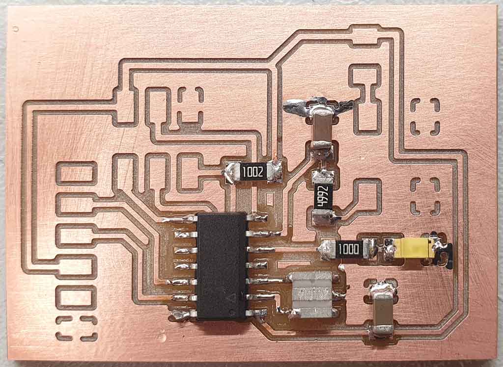
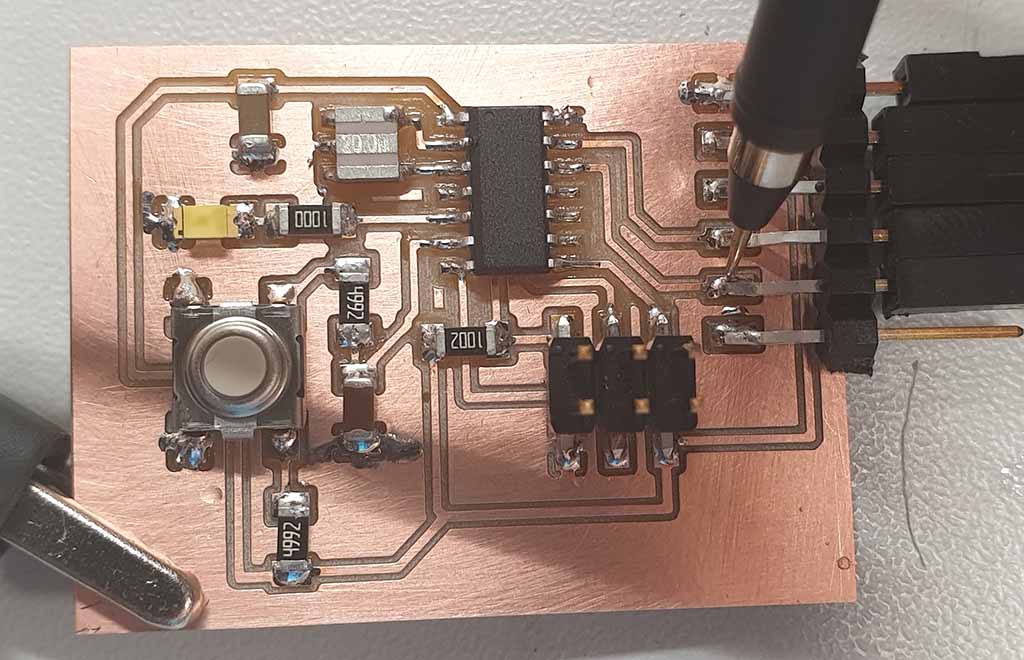
The board was done exactly like the FabTinyISP on week 5
At this point the design rule of 16mil(0.404mm) clearance can be problematic: The needed 0.4mm end mill bits were:
• 1. Lost in mail
and the two that we had received from the 20 ordered were
• 2. Broke.
A last-minute desperate decide to use the week 5 settings for the V-shaped milling bit was made. Luckily there were hundreds of extra those mill pits laying around.
The V-shaped milling bit cutting width was calculated from macroscopic picture to be enough wide.
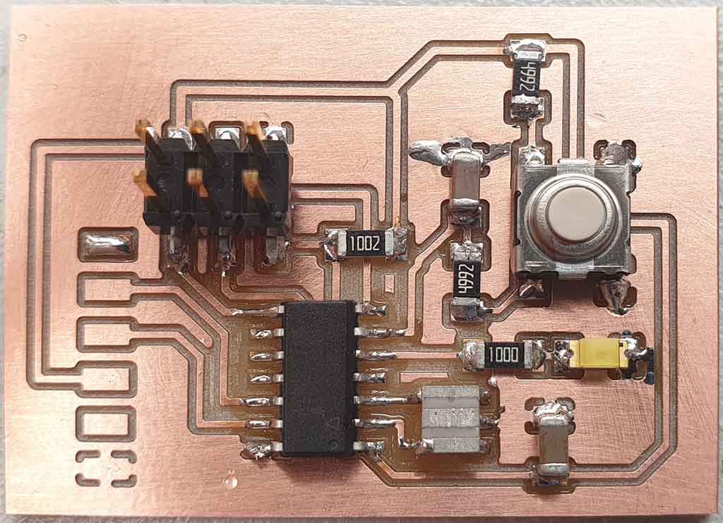
The parts were acquired from the mess stock.
The parts were:
- ATTINY44-SSU
- 20MHz Resonator
- AVRISPSMD 2x3-pin connector header.
- 1x6-pin smd side connector.
- 1x 10k ohm resistor-Pull up resistor for header vcc.
- 2x 49.9k ohm resistor-debounce voltage ladder
- 1x Omron 6mm Button-The extra part
- 1x 1 uF capacitor-debounce filter
- 1x 10 uF capacitor-attiny44a vcc filtering
- 1x 100 ohm resistor-Red LED current restrict.
- White LED-The extra part
The resistor for the LED was calculated taking to account the nominal 5V voltage. The forward voltage of the LED is 3.2V The resistor needs to have a voltage drop of 5V - 3.2V = 1.8V The Nominal current is stated on the LED is 20 mA. This gives minimum resistor value of R = {(Vin -VLED)/I} ==> {(5V - 3.2V)/0.03A} = 60 Ohm. Closest higher value resistor found from the inventory was 100 Ohm. This gives the usable current from Ohm’s law U/R = I ==> 1.8V/100 Ohm = 0.018 A = 18mA. This is below the absolute maximum DC current of 40mA of the ATTiny44A pins and can be used.
The same soldering rules apply as in the week 5.
Rules to hand solder PCB
• the hardest to the easiest
• the lowest to the highest
• the middle to the edges
Programming the board.
The Programming was done in Ubuntu 18.04.
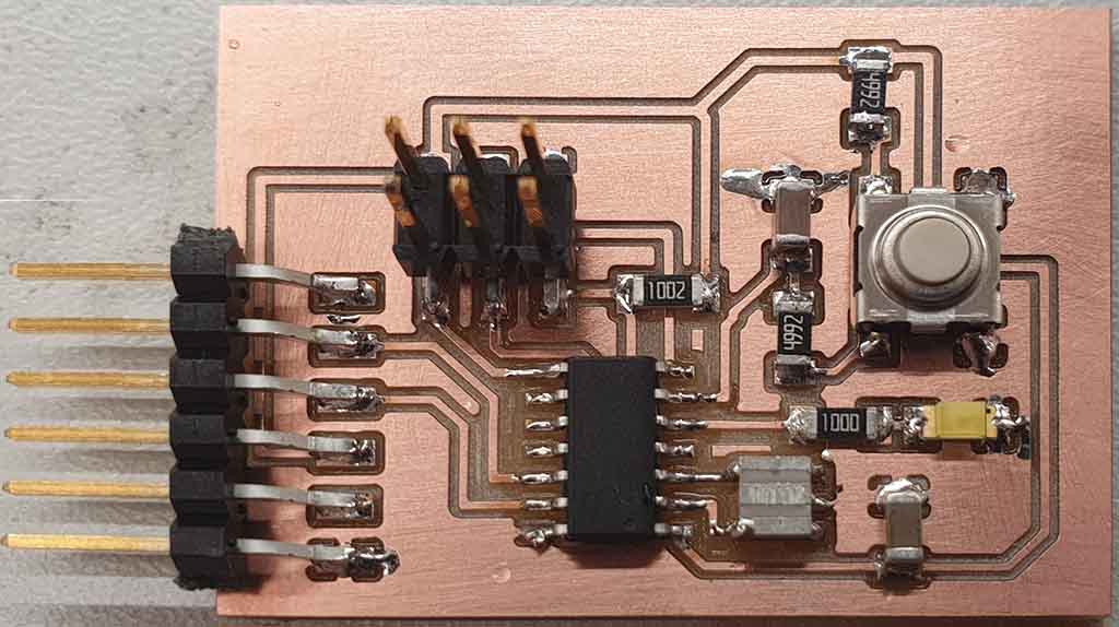
The hello.ftdi.44.echo.c was programmed to the board using the programming board,FABTinyISP that was manufactured in week5 The Board was connected with the 2x3 pin header to the FABTinyISP noting the place of the ground pin and orientation. Into the 1x6 pin header a 5V input was connected.
Programming the board in make in Ubuntu is easy. * First the fuses are burnt. The fuses are permanent bits that determines how the chip will act. Does it has a bootloader,
The programming was made in Ubuntu 18.04 via the make program. The necessary tools ( flex, byacc,bison,gcc,libsub and avrdude) was already installed to the ubuntu installation on week5.
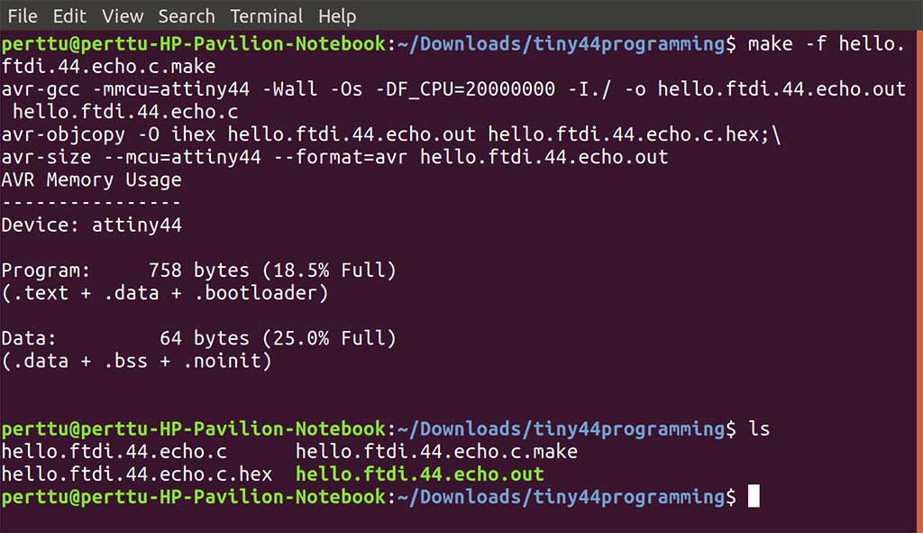
make -f hello.ftdi.44.echo.c.make The fuses are the bits that control the microcontroller setup. Such as the external resonator speed.
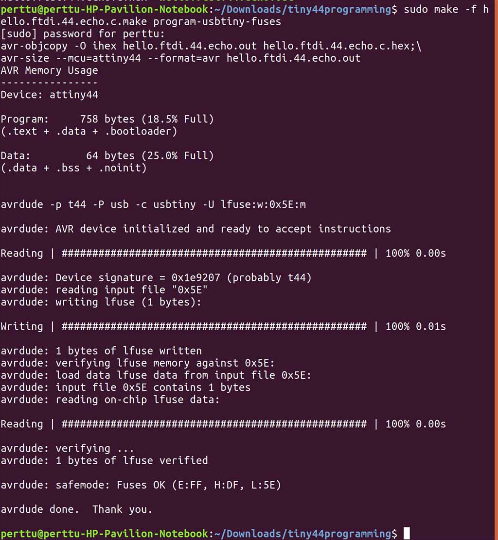
sudo make -f hello.ftdi.44.echo.c.make program-usbtiny-fuses Then the code is pushed to the board.
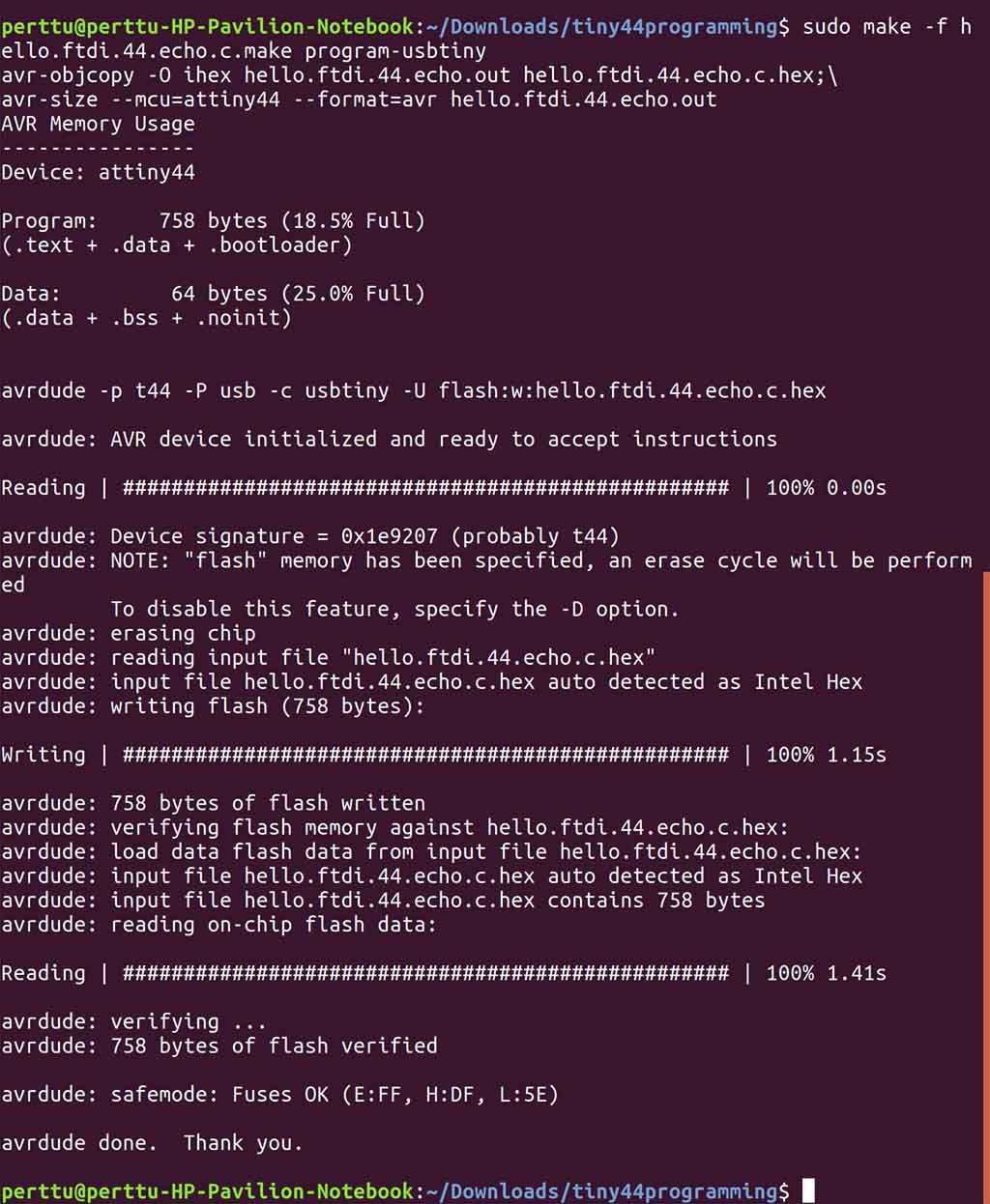
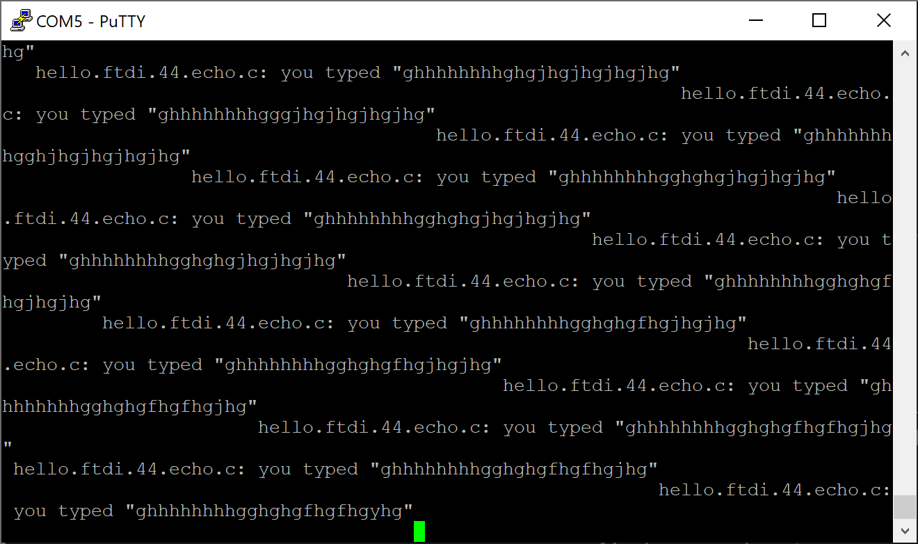
sudo make -f hello.ftdi.44.echo.c.make program-usbtinythe program is flashed to the microcontroller. To test the Echo program the board was connect to a FTDI cable to USB to read the Serial data.
2. Group assignment.
Group: Marjo, Gleb, Lucas and I.
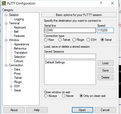
The group assignment was to measure and observe the working of the board. We measure the working of the serial signal coming from the TRX pin. The same setup was used as in the testing the boards. A FTDI -cable was attached to the board and putty connection was established to the board.
While probing the TRX line the letter U was pressed. in the UTF-8 unicode capital letter U is 01010101
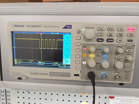
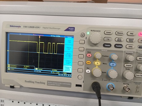
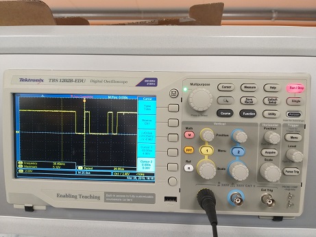
The baud rate was tested on the oscilloscope by measuring the time difference between number of bits. The oscilloscope reports the baud rate at 11.49kbits/sek. This is in the 5% tolerance of the used oscillator that managers the time that determines the baudrate. The baud rate is selected from the computer to be 115200 bits/sek. This gives as a 115200/114900 = 2.6% offser from the set bit rate.

All my designed files can be found in the Git repository