Week twelve: Output devices
Individual assignment
For this week, we had to design and fabricate a electronic board using an output device for our final project.
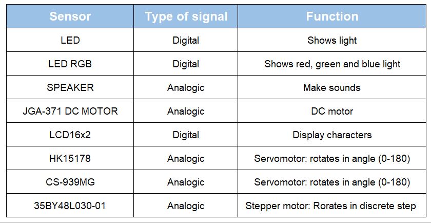
Our devices
We have several output devices in our laboratory
I decided to use JGA25-371 DC motor as output device, because i need to move the propeller in my final project (boat).
Reading the datasheet of the motor, i realized that needs 6V-24V to operate, but Attiny44 works with 5V, and maximum 60mA, so i have to use a 5V regulator Look the datasheet here
I worked with internal oscillator of Attiny 44, also i worked with pwm pins, 5 and 6. Look the datasheet here
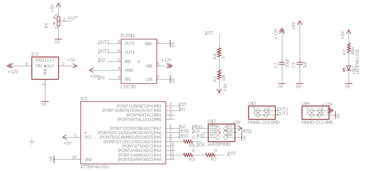
With this information i started to design the schematic board
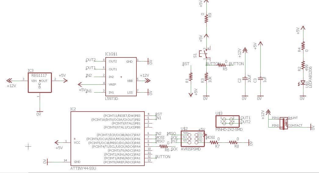
As you can see, i put a 5V regulator, it has one GND pin, one input voltage pin and one output 5V pin, you can't see the head in the schematic but when i tested continuity with the multitester i realized that is connected to GND.
Also i used 1 power LED, and add 1 button as input to attiny. I used 0 ohms resistors as bridge to pass across the traces. Also i put 2 capacitors, one at the entrance of the regulator and one at the exit. Maybe it doesn't seem like they are connected between GND and 5V, 9V but if you follow the 0 ohms resistors, which work like a bridge, you will realize that capacitors are connected to GND and 5V, 9V.
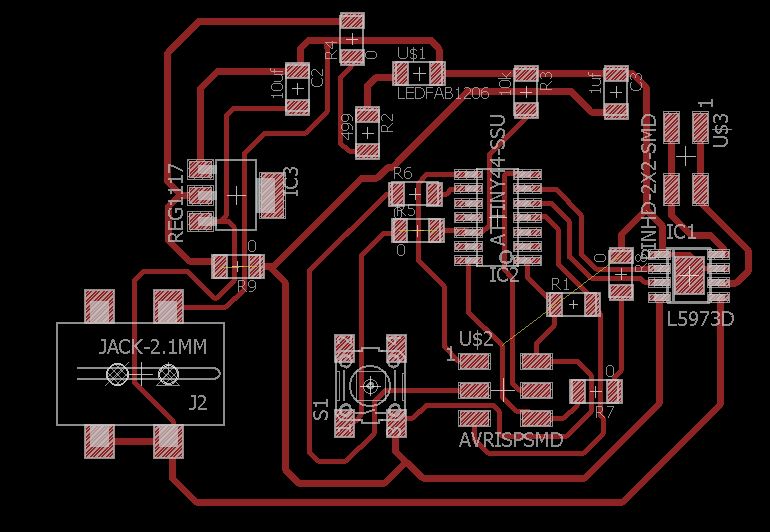
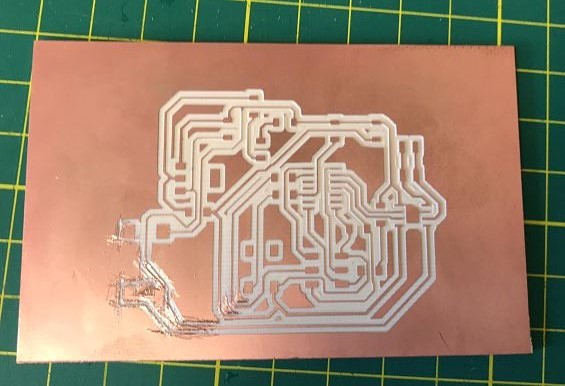
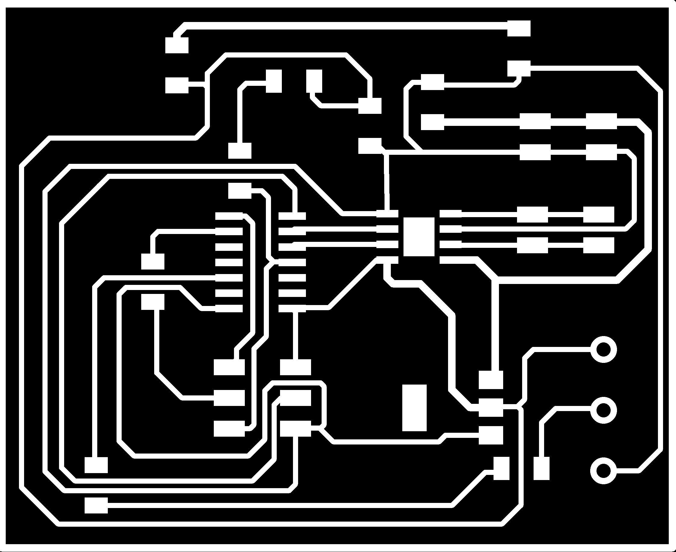
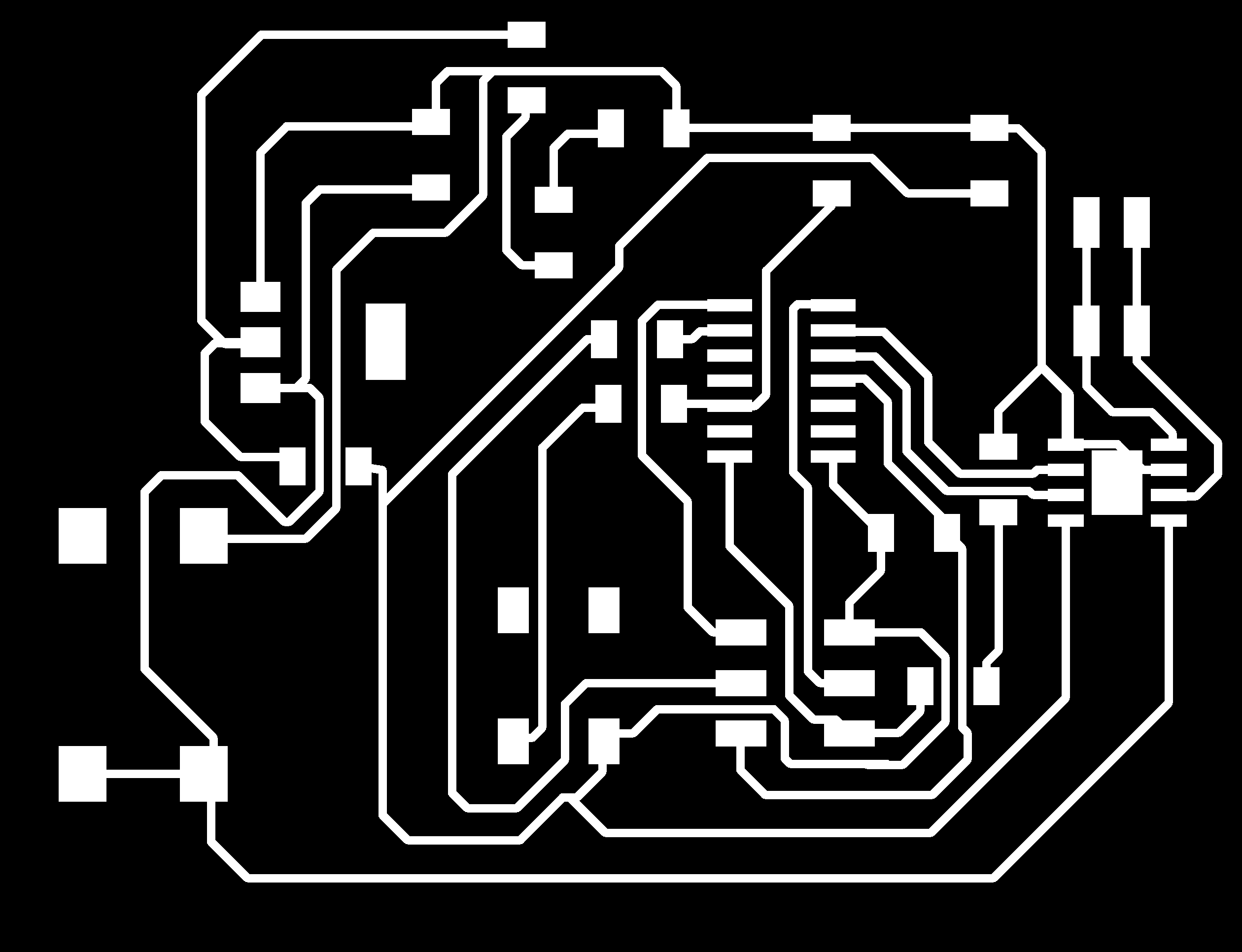
This was fabricated using Roland MDX where i used a conic mill of 1/64 ".
As you can see, I could pass 2 traces under the resistances, because in fab modules i selected diammeter of 1 mm. This allowed me to have a lot of precision and as a result and after several attemps, i was able to achieved this. Also, there are some handmade traces because the mill was weathered and i had to made these with a cutter.
Start soldering
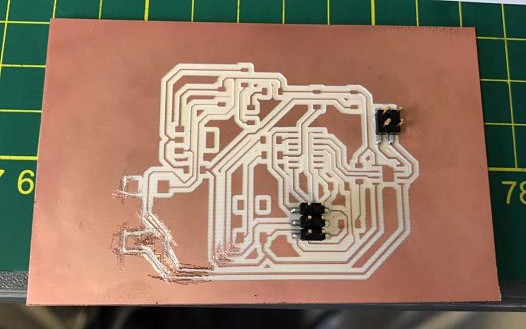
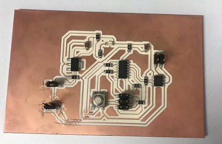
Result
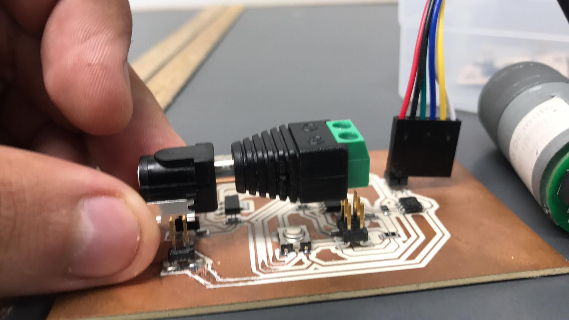
When i tried to solder the jack, i realized that there wasn't enough space for the jack and his adaptor to fit on the same board. I didn't realize the size of the jack adaptor at the design, so i decided to put a pin header.
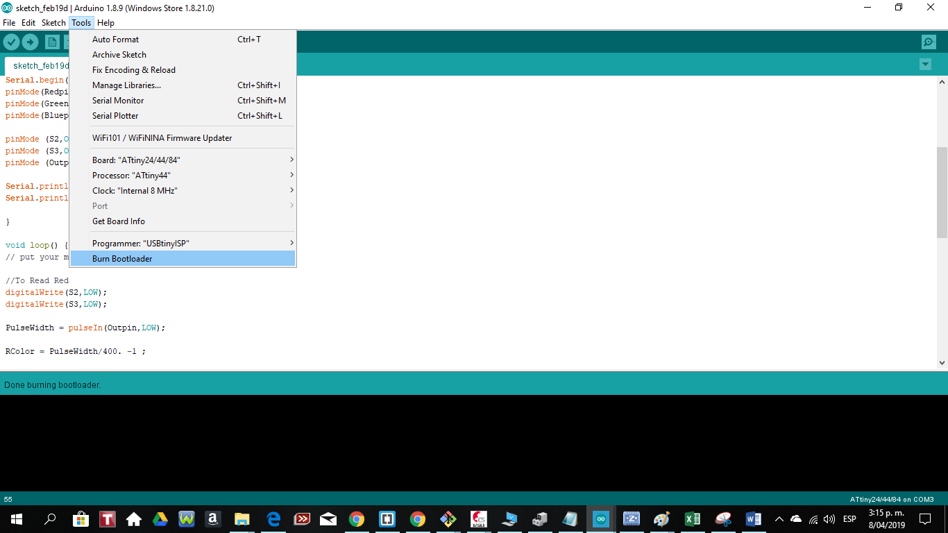
Once the board was finished, i used my ISP board from electronic's production week to burn bootloader.
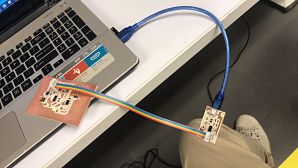
I discovered that i can program my board without FTDI and using my isp.
Coonected my board with isp
Select this option
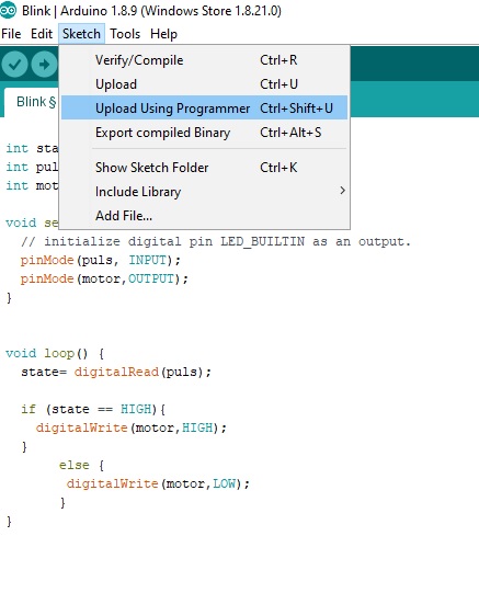
Program the motor to activates when input button is pressed and upload
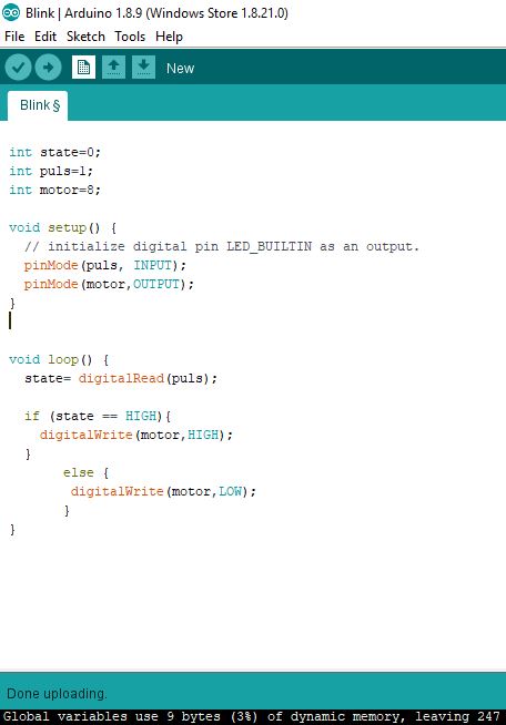
Code as text here:
int state=0;
int puls=1;
int motor=8;
void setup() {
pinMode(puls,INPUT);
pinMode(motor,OUTPUT);
}
void loop() {
state=digitalRead(puls);
if (state==HIGH){
digitalWrite(motor,HIGH);
}
else {
digitalWrite(motor,LOW);
}
}
Test
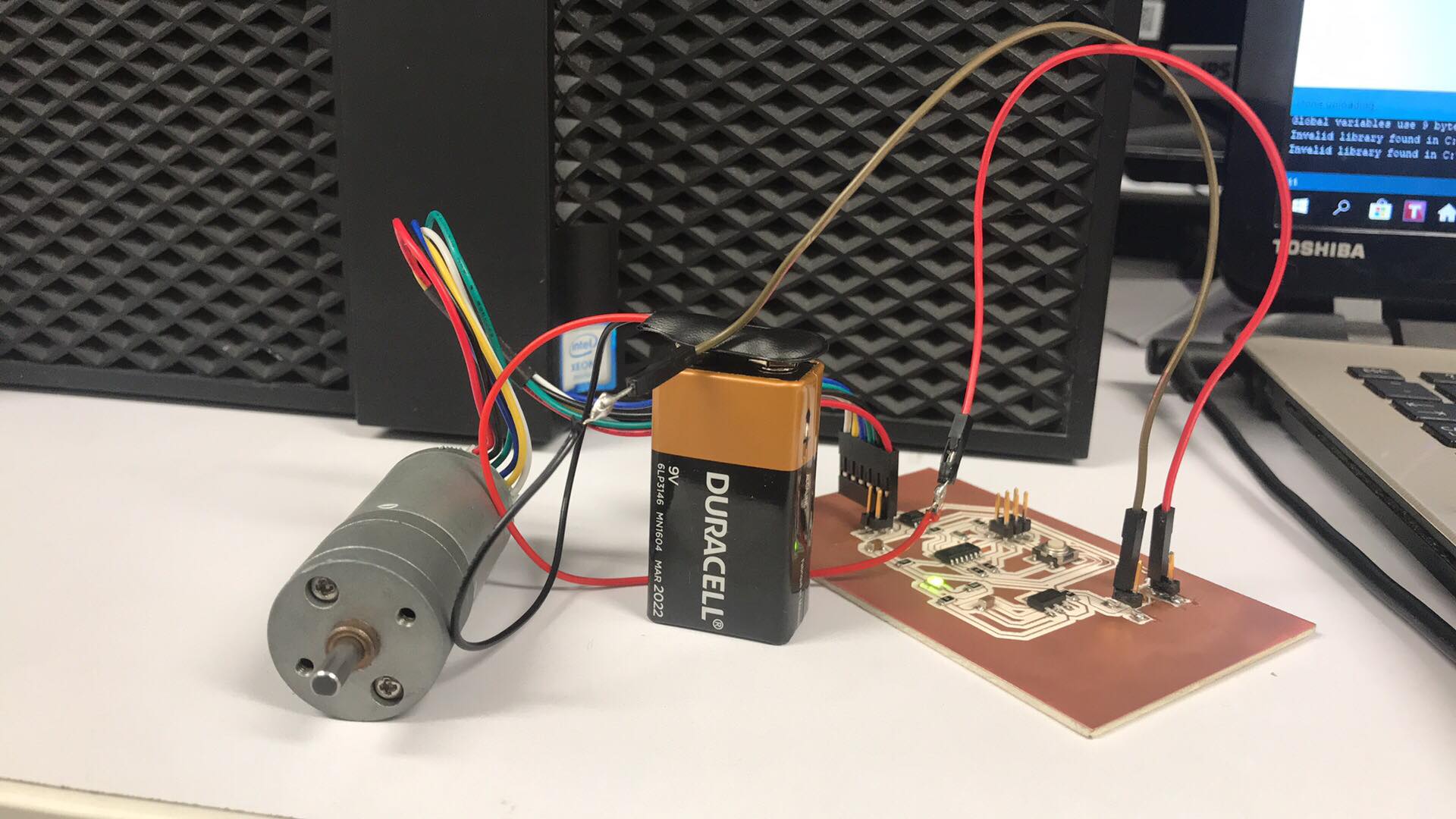
I used a 9V battery and DC motor
UPDATE
During the week of the assignment I had problems machining my electronic board, and after many attempts I got a board to work, but I did not cut it because I wanted to see if it worked well, besides, the jack was not SMD so I ended up using cut pinheads, which did not look very good.
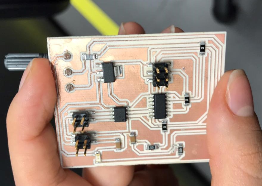
So I decided to make a better plate, and that allows me to have an analog signal to use it input to control the motor with PWM, so I made a new one and added a potentiometer, in addition, I corrected the errors of the previous one, and now I know Change the mill, it seems that when I made my previous board it was worn out.
As you can see in the schematic design, I added a potentiometer and removed the button, because I wanted to use an analog signal.
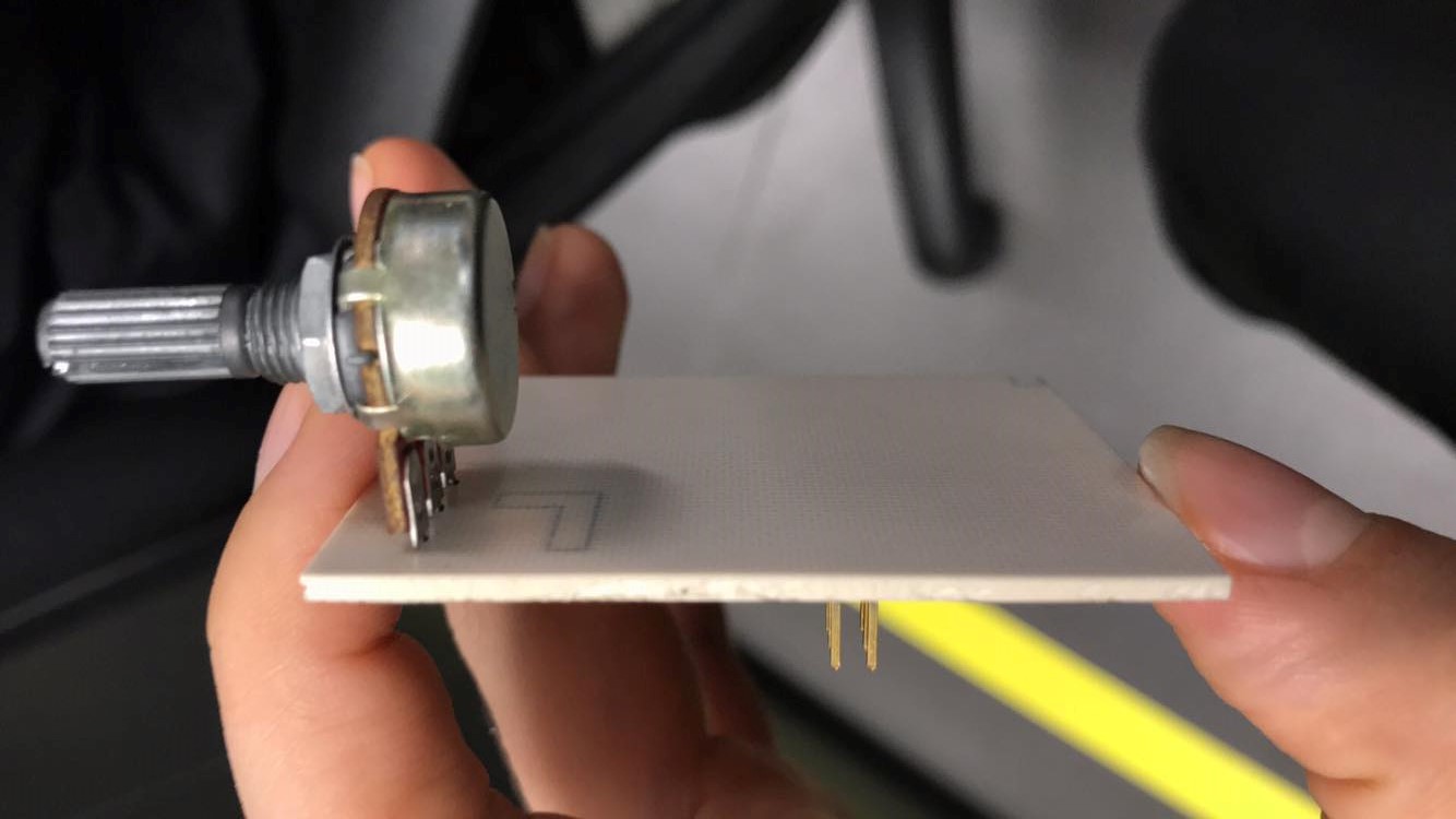
I did not find an SMD potentiometer so I used a trough hole. This time I managed to make a smaller board.
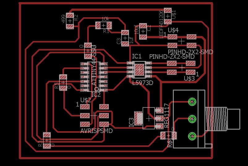
This time I worked with the board on one corner, to cut it and that others can use the rest of the copper plate

I soldered the electronic board using the heat gun, as always. Except the potentiometer, for this I used captive or electric soldering iron, and tin in roll. This is the result.
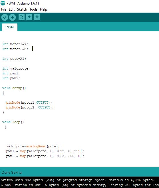
After burning bootloader using the ISP as the previous board, I programmed using the arduino IDE, first I declare the variables and pins, the output pins will go in 7 and 8 which is the arduino equivalence of the pwm pins 5 and 6 of the attiny44, in addition the potentiometer will be in the analog input 1. I create a variable for the analog reading of the potentiometer, and in pwm1 I use the map function to find the equivalence between the input range of the potentiometer (0-1023) and the output (0 -255). And in the variable pwm2 upside down (255-0), with this I will control the direction of rotation using the potentiometer and also the speed through the pulse width modulation.
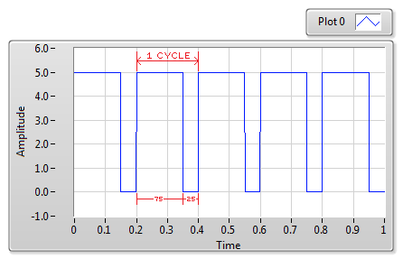
basically I play with the frequency and the duty cycle to create an analog signal from of a digital. For more information about PWM visit this link
int motor1=7;
int motor2=8;
int pote=A1;
int valorpote;
int pwm1;
int pwm2;
void setup()
{
pinMode(motor1,OUTPUT);
pinMode(motor2, OUTPUT);
}
void loop()
{
valorpote=analogRead(pote);
pwm1 = map(valorpote, 0, 1023, 0, 255);
pwm2 = map(valorpote, 0, 1023, 255, 0);
analogWrite(motor1,pwm1);
analogWrite(motor2,pwm2);
}
Here a video of the result
Group assignment
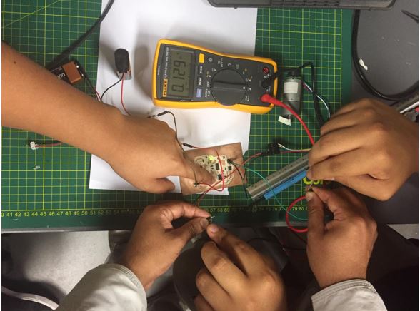
The group assignment for this week was to measure the power consumption of an output device.
My personal contribution was to measure the current consumption of DC MOTOR JGA25-371. I designed and fabricated this board. The value obtained is 0.129mA, this is due to the programing and the encoder that motor has. The motor was programmed to turn on when the input button is pressed.
To measure the consumption we needed to measure the circuit in series so what we did was connect the jumper GND of the motor to the board in its respective output, connect a loose jumper to the other output of the board, and another jumper loose in the other input of the motor, then we closed the circuit by connecting the test leads of the multitester to the jumpers, while someone pressed the button. And the value mentioned above was shown.
You can visit the CIT website to see all the documentation.
Downloads
To download the schematic design file, board design file and code file right click on the link and press "save link as..."
Schematic BoardBoard Design
PNG board
ON/OFF Code file in Arduino Schematic Boardv2
Board Designv2
PNG boardv2
PWM Code file in Arduinov
To see the complete development of the group assignment visit the following link that corresponds to the CIT page