Downloading link for my archives: Archives


Assignment 6 - week 6 - Mar 04
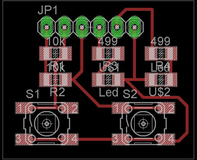
The assignment for this week is to redraw the the echo hello world board, adding at least a button and a LED to the original design, using some of the proposed software. then make it with the Modela MDX20 and soldering the components.
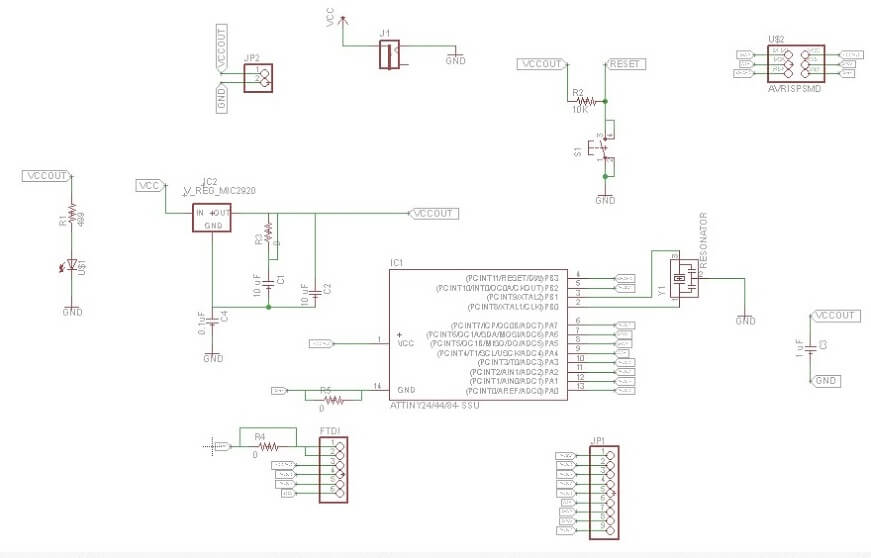
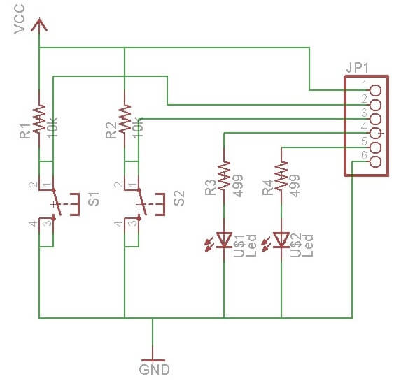
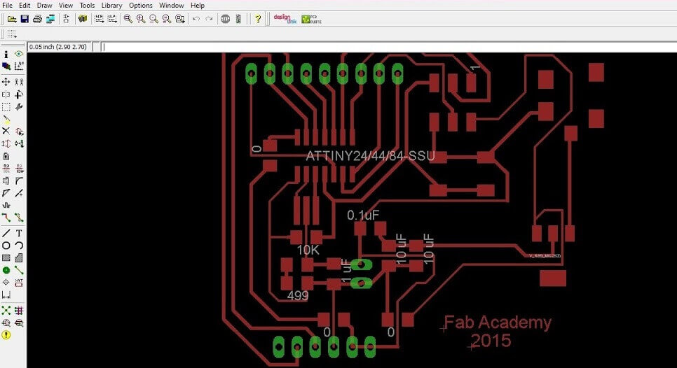
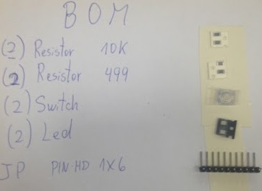
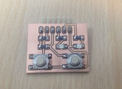
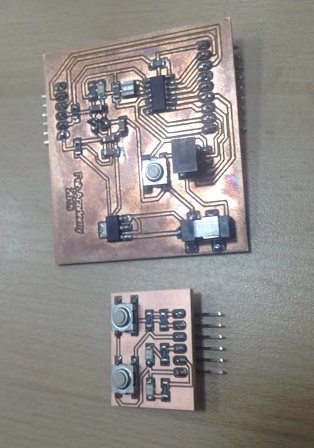
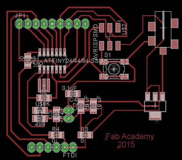 In the design of this second board, we present two LEDs and two switch with their respective resistors for proper operation.
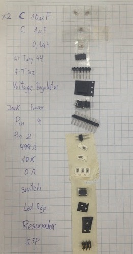
We resistances of 499 ohms Fab_Hello library, and encapsulation type 1206 to use them with the LED diodes having the same package 1206.
In the case of the switch encapsulation was 6mm and manufacturer OMRON, with their 10k ohm resistors with the encapsulation type 1206. The switch needed input voltage VCC , so is that we implement one of the pinhead 1x6 . For LEDs and switches , connect the same GND.
The 6 pinhead were distributed as follows: 1 VCC , 2 Switch1 ,3 Switch2, 4 Led1, 5 Led2 , 6 GND.The distribution on the plate was simpler than the Hello controller board .
In the design of this second board, we present two LEDs and two switch with their respective resistors for proper operation.
We resistances of 499 ohms Fab_Hello library, and encapsulation type 1206 to use them with the LED diodes having the same package 1206.
In the case of the switch encapsulation was 6mm and manufacturer OMRON, with their 10k ohm resistors with the encapsulation type 1206. The switch needed input voltage VCC , so is that we implement one of the pinhead 1x6 . For LEDs and switches , connect the same GND.
The 6 pinhead were distributed as follows: 1 VCC , 2 Switch1 ,3 Switch2, 4 Led1, 5 Led2 , 6 GND.The distribution on the plate was simpler than the Hello controller board .
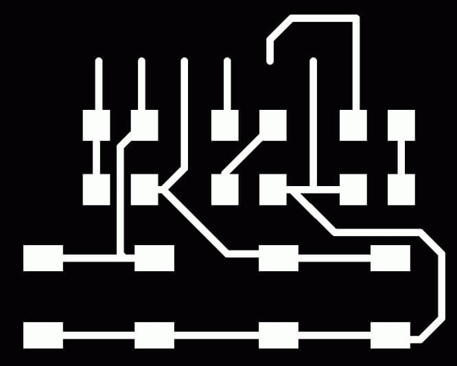
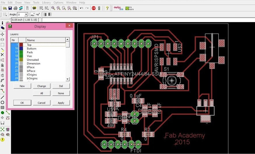
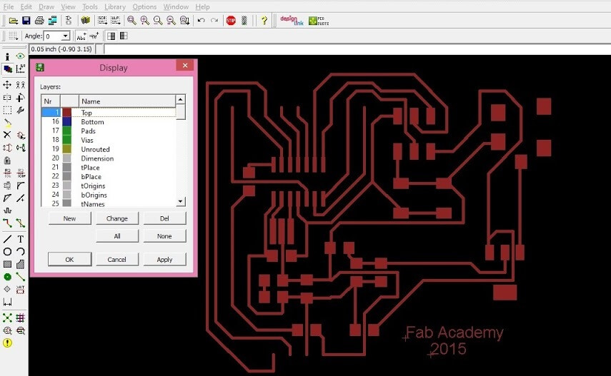
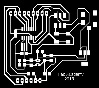
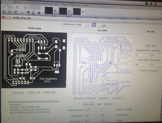
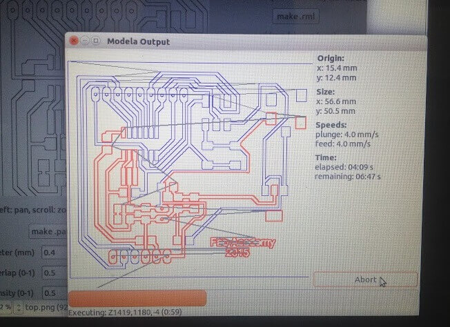
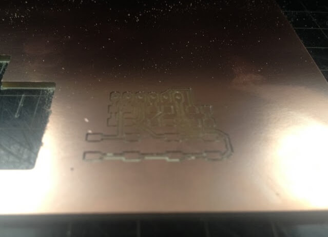
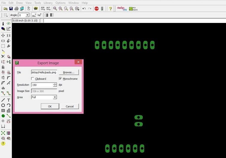 We must be clear what are the names and where the images in png for milling and for cutting.
To continue the Models must have the 2 images in PNG, the image of milling, cutting and image.
We must be clear what are the names and where the images in png for milling and for cutting.
To continue the Models must have the 2 images in PNG, the image of milling, cutting and image.
Downloading link for my archives: Archives
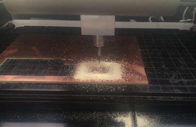 Drilling: Before using any machine or tool must check the voltage with that work. In this case the drill works with 120V and has a transformer for this.
Then in a test board drilled with a next to the size or pads milling tool, once we confirm the size or milling tool, adjust the hole and proceed to drill a pad at a time, and after performing cleaning each hole .
Drilling: Before using any machine or tool must check the voltage with that work. In this case the drill works with 120V and has a transformer for this.
Then in a test board drilled with a next to the size or pads milling tool, once we confirm the size or milling tool, adjust the hole and proceed to drill a pad at a time, and after performing cleaning each hole .
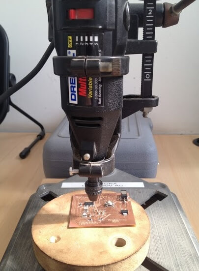
 Once finished, clean the work area and proceed to weld.
Once we have the board ready , go to the schematic of the circuit and type RUN BOM to display the list of materials, and to apply. Since the components proceed to weld.
Once finished, clean the work area and proceed to weld.
Once we have the board ready , go to the schematic of the circuit and type RUN BOM to display the list of materials, and to apply. Since the components proceed to weld.
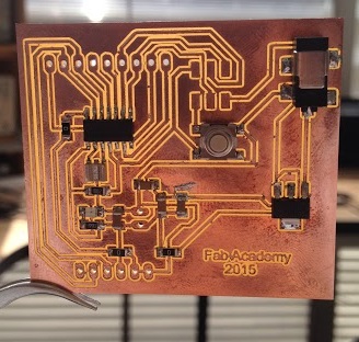
 Sodering: We must consider the polarity in the case of leds, and try not to confuse the capacitors.
The technique we use for welding is to put some tin board on one pin component so sure, then solder the other pins, and ultimately reinforce the first pin.
Communication solder pins ISP to last for comfort.
We verify the continuity constantly using the multimeter.
Sodering: We must consider the polarity in the case of leds, and try not to confuse the capacitors.
The technique we use for welding is to put some tin board on one pin component so sure, then solder the other pins, and ultimately reinforce the first pin.
Communication solder pins ISP to last for comfort.
We verify the continuity constantly using the multimeter.
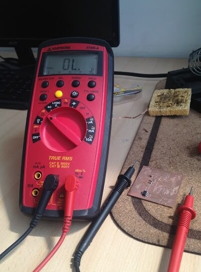 By joining the points on the screen should show a resistance value, and additionally must make a sound. If the tips are joined not worth OL shown. We perform continuity test on both boards.
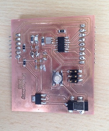
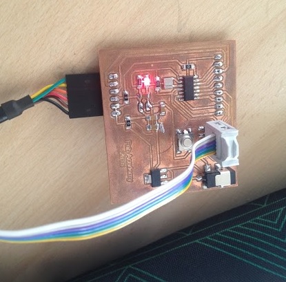
For the controller board with the help of FABISP, we charge a test program from TERMINAL in Ubuntu, which turned us successful, and as proof, the red LED is lit on the board.
Therefore the controller board ATTiny44 is ready to be programmed.
By joining the points on the screen should show a resistance value, and additionally must make a sound. If the tips are joined not worth OL shown. We perform continuity test on both boards.
For the controller board with the help of FABISP, we charge a test program from TERMINAL in Ubuntu, which turned us successful, and as proof, the red LED is lit on the board.
Therefore the controller board ATTiny44 is ready to be programmed.
I feel that in this week I just scratched the surface of the wealth of skills, techniques and tools needed for producing good electronic designs. The PCB layout alone looks really like an art that will take lots of practice to be mastered. For which the many options available really require more dedicated time to be full understood.