
Claudia Aguilar
FAB ACADEMY 2015

REDRAWING AN EXISTING BOARD
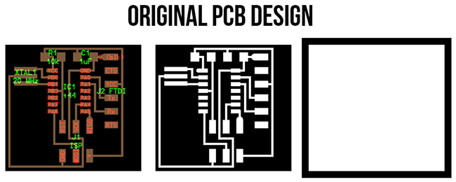
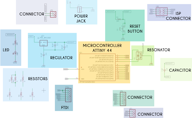
For this weeks assignment we are redrawing the Echo Hello World Board which is a programmable board. What it does is a simple example of communication, it has just a few parts: micro controller( the computer chip), resonator to tell time, a resistor (reset) that tells it when to turn on, a capacitor that filters power a connector to communicate and a connector to programming (ISP header). With this design the computer can talk to the processor and the processor to the computer so we can program it to do what we want. In the original board there's a number of pins free so we can use them to read an input and make an output.
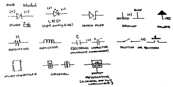
To start, I went back to basics, as I know less than nothing about electronics I started reading "Electronics for dummies" which helped me understanding the basic concepts and getting into my mind some of the most used terms. Next you can see some of my annotations.
Now that I know some of the basics I took the time to analize what we have to do and how to do it.
Being this my first time working with electronics in general, I took my time to at least try to understand what is everything about, for this I analyze all the components in available and also search or ask for mentoring to know what else I can do with everything I have.
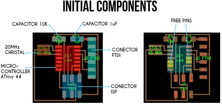
The sugested components to add to this board are LED (Light-emitting Diode) and a button
For this assignment one of the most important things is to know and understand how the microcontroller ATtiny44 is being used. Thinking of this I analyze the microcontroller and graph it on the next scheme.
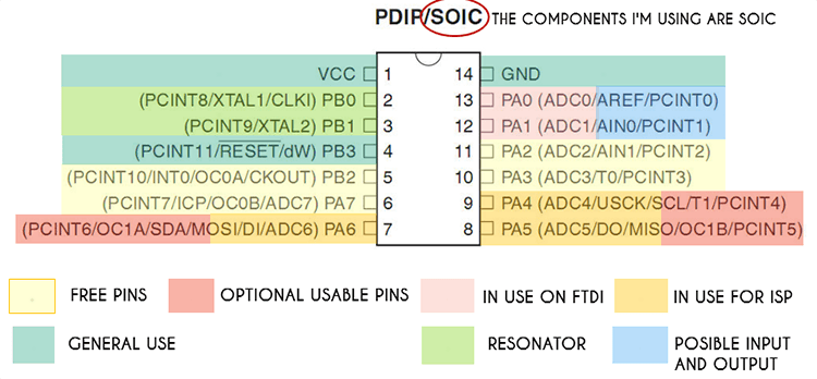
Once having this done I also found this scheme that shows all the characteristics of each of the pins of the Microcontroller..
With this understanding and thanks to the members of my laboratory support, I got to realize that I can not only use the free PINS in the micro controller but I can also use some of the pins that are being used in the ISP as this will be used only for the moment of programing and then they are available for other uses after programming.
This all generates the idea of creating not only a board with a LED and a button but better a "MULTI PURPOSE BOARD" that can have a general use being programmed and having other small boards connected to it as Inputs or Outputs.
As I mention in week’s 4 assignment, we can use EAGLE to design the PCB so this is the software I decided to learn and use.
I found this video tutorial pretty clear and easy to learn, it helped me to understand the program and see how to use it.
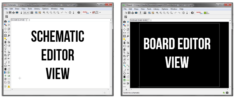
To start I got clear that working with EAGLE and designing PCBs was about two things: electronic scheme and a board with clear routes and components together. Relating this to my architectural career helped me a little as in softwares like AutoCAD you also use two views the model view which is like the schematic editor and the Layout which is like the Boards Editor view. As an architect it was also useful to analyze the components and the routes as objects with special characteristics that also have spatial requirements just like designing a house: analyzing the rooms and studying the people's distribution paths to go from one to an other.
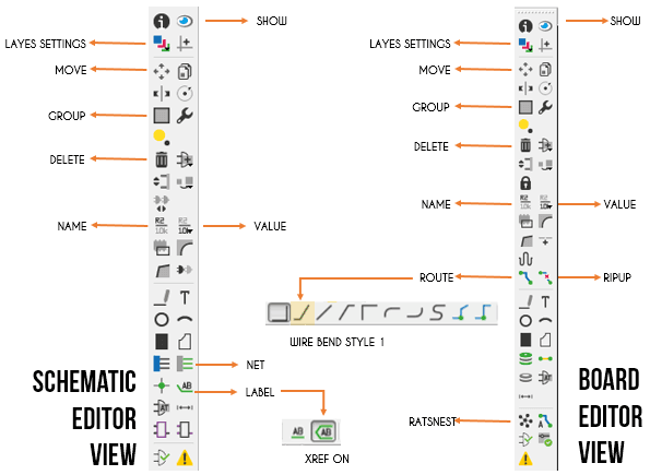
With my little knowledge of EAGLE this are the tools I use the most to make my design in schematic and Board view.
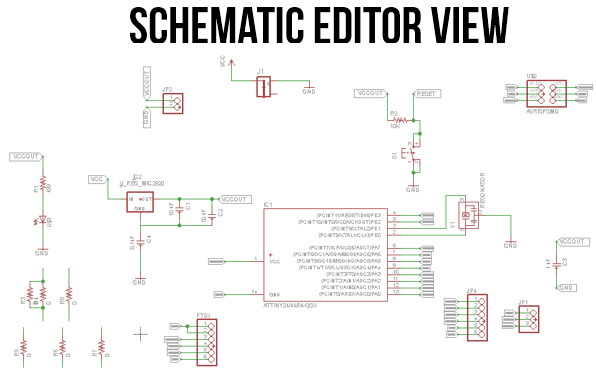
Here is a graphic description of the design in schematic view.
To generate this schematic I studied the basic symbols I was using starting from the standard components the Hello.Board already had. Next you can see my annotations.
The Schematic Editor is used to edit a schematic (*.sch). In this case and taking into account the previous microcontroller schematic I added more connectors to make this a MULTI PURPOSE BOARD so I just have to design new boards with inputs and outputs like lights, motors and sensors between others. I also added a light to show it's functioning and a reset button.
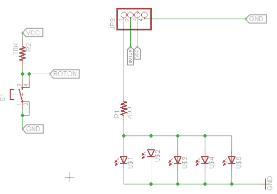
LED Board design.
To make a probe of its functioning I also made this small board that contains a state button, a pull up resistor, four LEDs in parallel connection and a current limiting resistor for them.
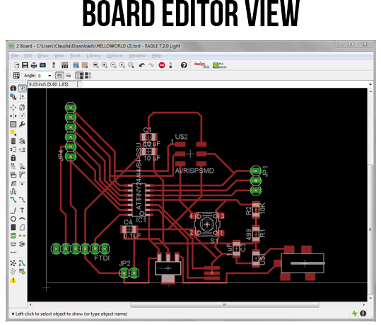
The Board Editor is used to edit a board (*.brd).
One of the most difficult things for me was to understand the connections and spatial distribution of the components. I realize this couldn't be done right just by watching the schematic or the board design so I also saw the real components and understand how they work and see its shape to make some important decisions at the moment of making the PSB design. For this I found useful a previous scheme I made in week 4. Watch it here.
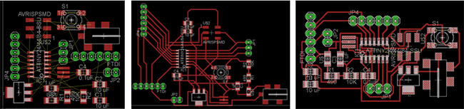
I had to make almost 10 different boards, first of all to understand how to use the program and then to improve the board design itself.
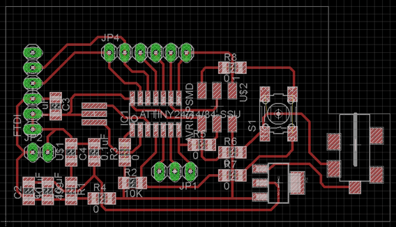
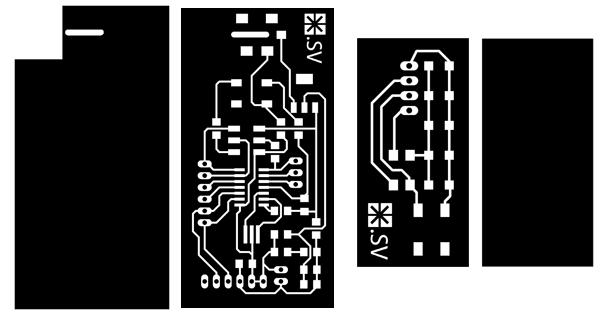
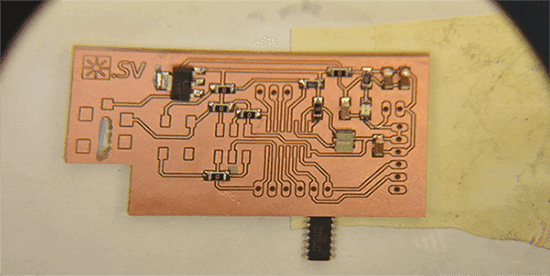
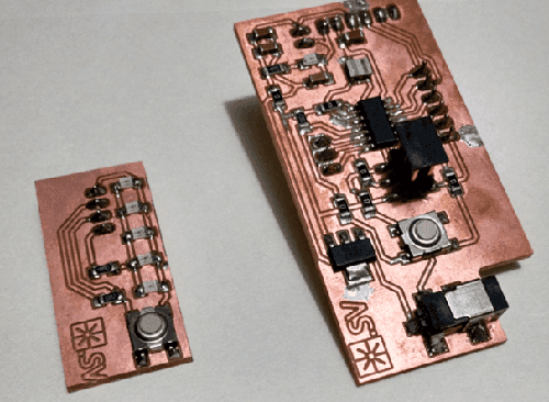
FINAL PCB
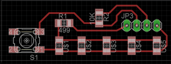
FINAL LED BOARD
Even if I did this in the week’s 4 assignment, in this occasion I had troubles to personalize my PCB and I wanted to share it.
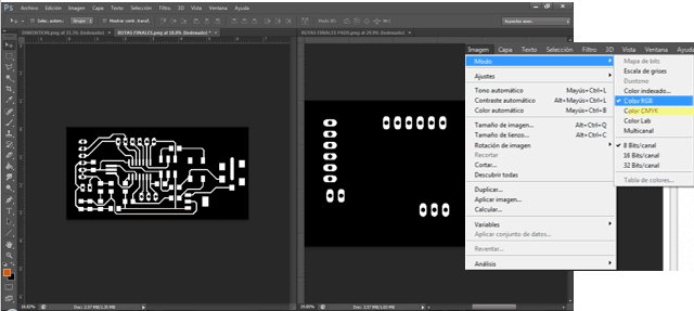
I try to edit the PNG image exported from EAGLE in Photoshop and I had to calculate right the exact place to put the connector paths, I needed to edit the view for this and I couldn't because I couldn't create layers. Then I saw it was because the image was indexed, so it didn't allow me to do it. I searched for the solution and it was easy as going to the image menu and changing the Image mode to Color RGB or CMYK. After doing this I could edit it fine and then checked the image size and resolution and save it as .PNG
This is how the PCB ended up:
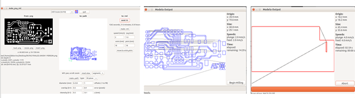
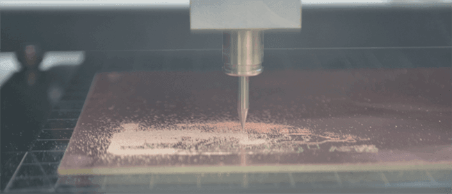
The first time I mill the board there was a mistake in the upper right corner because the board was down in that place. So without changing the parameter I calibrate again the mill in this point I send again the path and .rml and it milled find the place it hasn't mill before and mill for the second time the routes it had already milled.
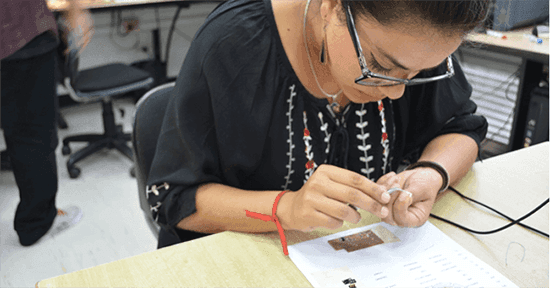
First of all was selecting all the components to solder and placing them orderly not to be confused in the process.
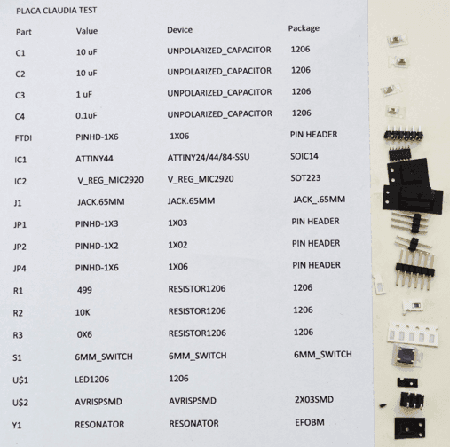
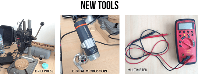
For this design I got to use new tols to make the header holes (drill press), to see better the solded components and paths (Digital Microscope) and also to make a continuity test in the board (Multimeter).
This is the first PCB which I had to make again because there was a continuity error that I couldn't fix.
This are the first boards I mill.
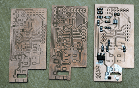
This are the last boards and they worked fine.
You can download all of this the Eagle and PNG files in here.
See more pictures in here:
A video of my process in here:
A video showing my boards soldering with a digital microscope:
Click here to see this class content
Click here to see this class recorded video