
Claudia Aguilar
FAB ACADEMY 2015

ASSIGNMENT: Make the FabISP
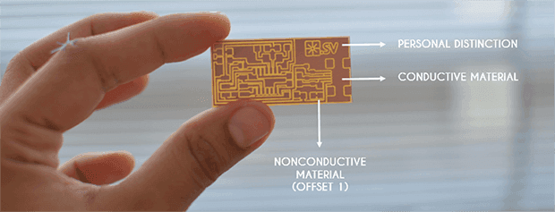
This week's assignments is to make the FabISP an In-System Programmer so I decided to use the design of David A. Mellis and personalise it so I can distinguish it from the other ones. Being a new topic for me I tried to document everything as detailed as possible to understand and refer to future questions.
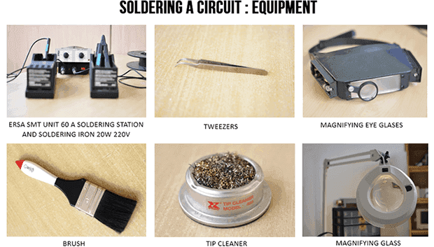
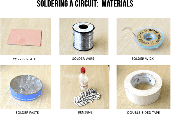
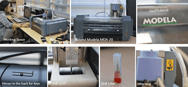
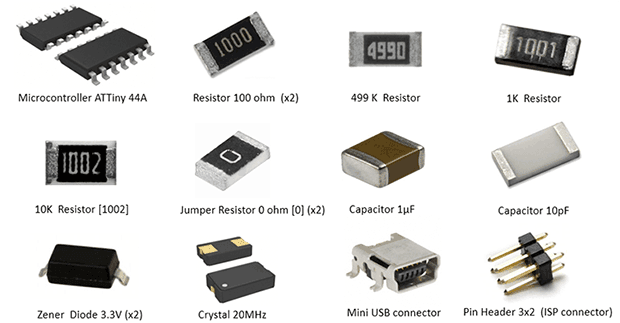
For this assignment I'll be using the next equipment and materials:
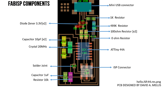
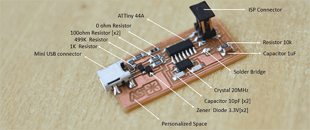
A FabISP is an in-system programmer for AVR microcotrollers, designed for production within a FabLab. That is, it allows you to program the microcontrollers on other boards you make, using nothing but a USB cable and 6-pin IDC to 6-pin IDC cable. It's based on the USBtiny and V-USBfirmwares, which allow the ATtiny44 to perform USB communication in software. Programming can be done through avrdude. The schematic (PDF) is super simple: USB connector, ATtiny44, and 6-pin ISP header, with assorted passive components (sourse).
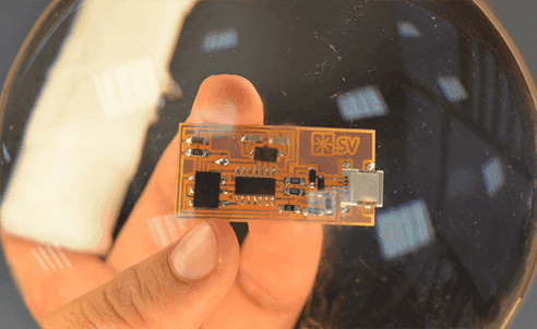
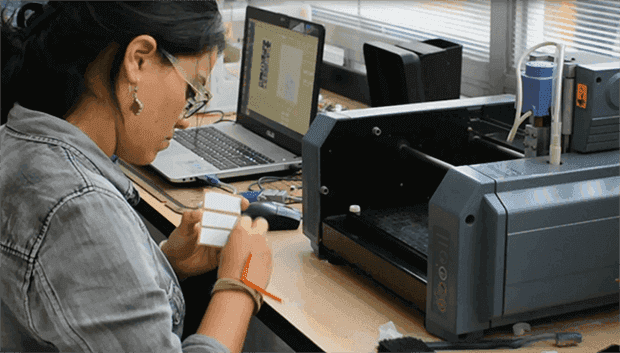
For this I’m making a PCB “Printed Circuit Board” with the Roland Modela over a Cooper Plate that will basicly generate a surface of conduct and non conduct material providing an electrical connection between the different electronic components and also a firm base to contain them. This is a device that will allow me to program other devices.
For this assignment we have the opcion to download PCB design but you can use EAGLE to design your own PCB.
This are the steps I'm taking to create my FabISP:
1. Download and customize the PCB design.
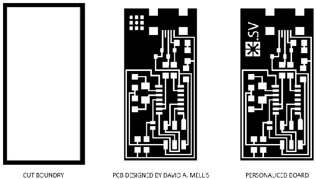
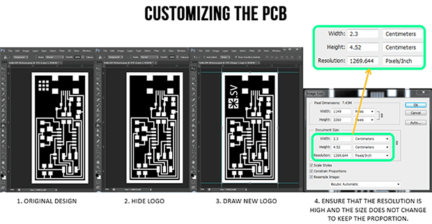
For the customization of the PCB one of the most important things is that you have to be sure not to change the size of the board at the moment of saving it besides you have to check the Resolution of the image because the Modela prints better at high resolutions. In this case I'm keeping the original resolution of the image 1269.644 Pixels per inch and The process I took to personalise it was just taking of the top left corner logo and putting instead mine using Photoshop.
I tried the customizing at first without thinking about the thickness of the lines, and then when I went to the Modela and Try to print it the image of the logo wasn't showing because it was to small but I didn't notice it until I send it to make "rml", I had to try at least three times until I finally got the right size and the logo was finally shown fine. The principal problem was with the diagonal lines as I took the same size of the orthogonal ones but it wasn't the same at the time to make the RML.
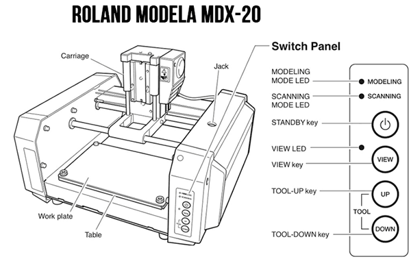
2. Clean and attach the Copper Plate with double-sided tape in Rolands Machine base.
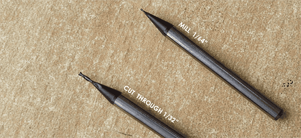
3. Check the drill in the Modela and change if necessary. For tracing we use the 1/64
4. Reset the coordinates and move the drill over a Copper plate’s corner using Modules, once there lower the drill until the tip is just touching the surface.
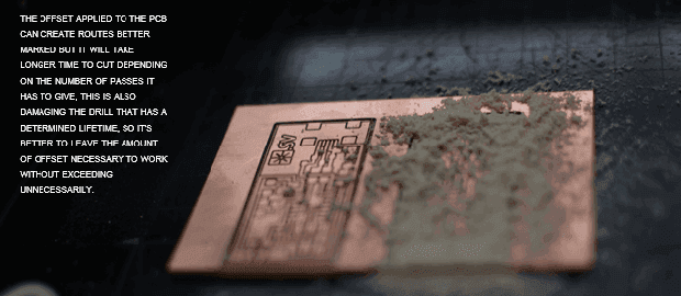
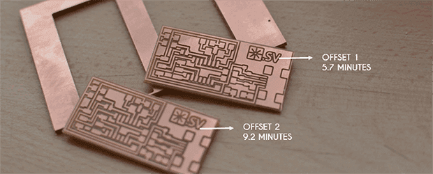
5. Once in the right coordinates charge the PCB PNG design in the Fab Modules testing the offset 1, generate the path and check the milling time.
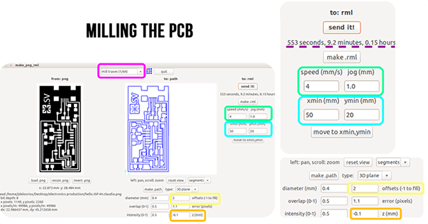
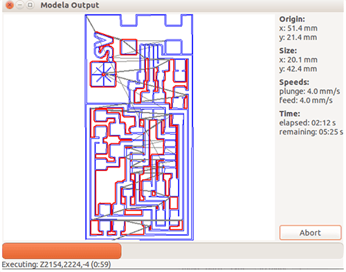
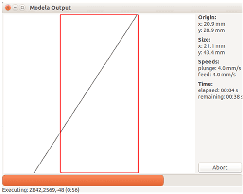
6. Send it to mill the trace.
7. Clean the surface and see results.
8. Repeat steps 4 and 5 to mill this time with offset 2, check the time.
9. Clean the surface.
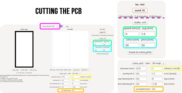
10. Change the drill to a 1/32 and cut repeating steps 4 and 5 but this time it isn’t necessary to change the offset.
11. Extract cutted boards.
12. Clean work space.
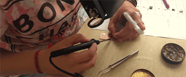
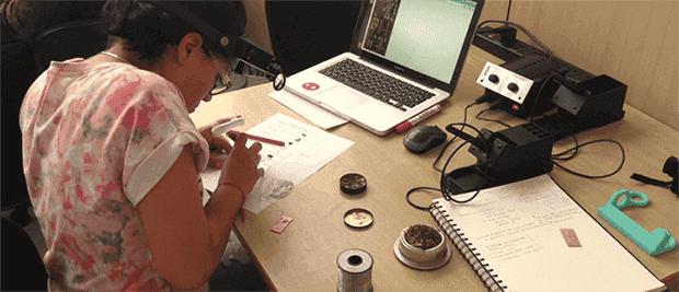
13. Move to the soldering station workplace and solder the components following the example. This happened to me actually, I took the amplifying lens to check if everything was allright and I noticed that the crystal wasn’t well attached to the board, I fix it and then it worked.
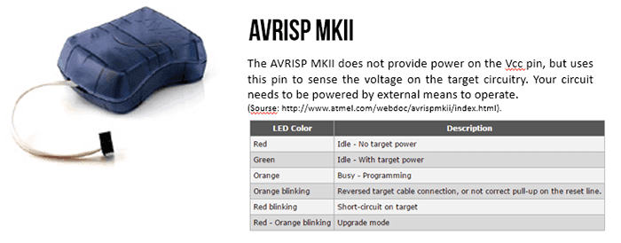
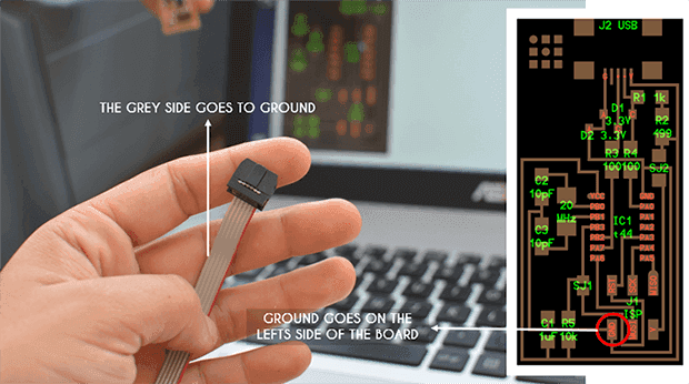
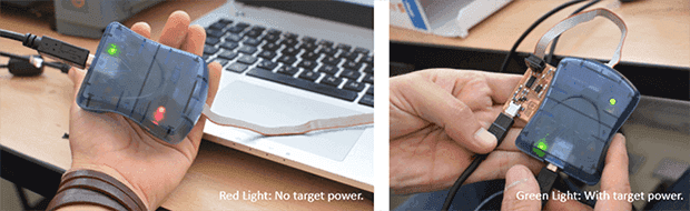
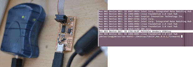
14. Connect to the AVR and see if it is recognised, check for soldering joints if not so. For more information about the AVRISP mkII click here.
15. Program de FabISP. You can see here the programation file running Make clean/Make hex/Make fuse.
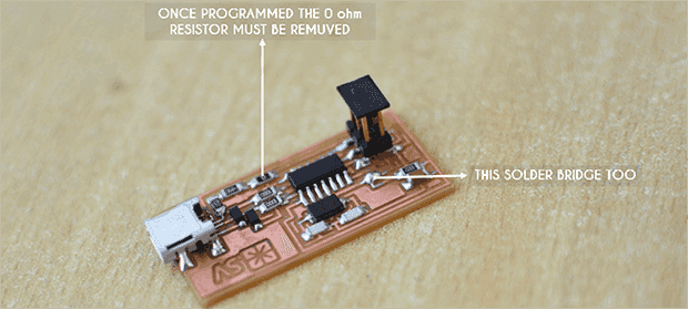
16. Once programed the board remove the 0 ohm resistor and the solder bridge.
After this whole process I've learned things I've never heard before like ISP - In System Programer; PCB - Printed Circuit Board and EAGLE - Easily Applicable Graphical Layout Editor, in the progress of the course I'll be learning and applying more of it.
Next you can see more pictures of the process:
Here is a video resume of my process:
I took a video of our instructor José de los Ríos explaining us how to use the equipment, it's in spanish so I shared it with the Latinamerican FabLabs.
Click here to see this class content
Click here to see this class recorded video