Week 6 : Electronics design
Design
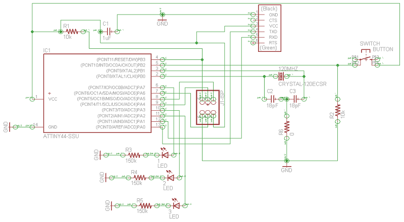
This week I had to design myself the echo hello-word board so it was a first for me as I had never designed
electronic circuit. We also had to put at least one LED and one button. I decided to use eagle so
I began by watching this
tutorial
and this pdf
was very helpful also.
After that I started to add components in my schematic on eagle.
To choose the resistor for the LED I used a website called "ledcalc" which calculates the value when
we enter the parameters of the circuit. Concerning the button, I chose a resistor and then verified
that it was appropriate. R6 is just a bridge that I needed to draw the board.
Some of those components were already in a library of eagle :
- R1 and R2 (resistor 10k) with package R1206
- R3, R4 and R5 (between 150 and 180 ohms) with package R0805
- R6 (resistor 0 ohm) with package R1206
- C1 (capacitor 100nF) with package C1206
- C2 and C3 (resistor 18pF) with package C1206
I found some of the others in the
fab.lbr :
- Microcontroller which is called ATTINY44-SSU
- J1-ISP which is called PINHD-2x3-SMD
- J2-FTDI which is called FTDI-SMD-HEADER
And for the last three, I had to draw the package myself because I didn't find them :
- Crystal 12ECSR SMD (12MHz)
- Button with 4 pins (I flattened the pins)
- 3 Yellow LED with two pins (I folded the pins)
************************************************************

It can happen that you want to use a component that you don't find the package in any library, so I have
detailed below how to create a device that suits your component :
- Library -> Open... -> Choose the good one in your browser
- Click on Package -> In the window "New:" type the name of your
new package -> OK
- Draw the pads after measuring your component
- Write the important informations about the pins and what you want
- Be careful about the colors, they are important !!!
- Save
- Do the same for the symbol or just find one that fits in the library
- Click on Device -> In the window "New:" type the name of your
new device -> OK
- Your device is empty
- Add -> Choose the good symbol in the list -> OK
- Put your component in the middle
- On the right there is a button "New", click on it
- Choose the package you designed -> OK
- On the right there is a button "Connect", click on it
- Connect the pins of your symbol with the pins of your package -> OK
- Save -> It's done, you create your new device !
************************************************************
I opened the associated board, I placed my components in the frame and then ... I had lots of wire in all directions that crossed. It looked like nothing, it seemed impossible. The only advice I can give is ... to stay calm and patient and take time to connect each component one by one with the routes. And in case of impossibility, or if you are tired : use bridges x) . I finally succeed after a very long perseverance (see above :).
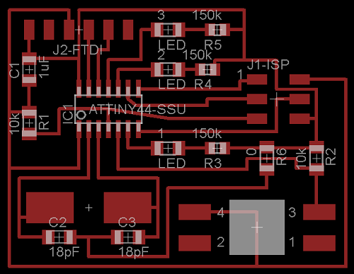
So I checked my circuit by clicking "ERC" (Electrical Rules Check) and "DRC" (Design Rules Check). In the
Clearance tab of the DRC window, I changed the minimum distance between all entities in order to put
a bit more than the size of the tool (18inch) that I would use to mill the pcb. I clicked on "Errors" to see
what was wrong and I corrected the errors detected.
I extracted the board into a png image and I drew the outline on inkscape
(paying attention to the tool used for milling after).
Milling... or not (:
I had properly prepared my G-code on the Fabmodules as I did during the week 4 and I was ready to
mill my pcb when the LabManager suggested I try something I had not done yet. He offered me to
draw copper tracks by chemical reaction (etching).
This required a special pcb covered with a protective lacquer photosensitive (sensitive to UV radiation).
And for that, no need to FabModules, just a
pdf of the board.
The various steps are described below and the eagle file is here.
Step 1 : We printed the pdf on a transparent sheet (in mirror mode), this is the typon.
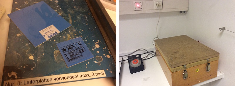
Step 2 : We cut the pcb with a "cutting pcb" at the circuit size.
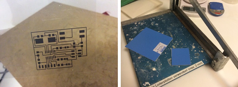
Step 3 : We removed the protection of the pcb (light off)
Step 4 : We put the printed sheet on the pcb and put the two inside the box where they were violently
illuminated by UV lamps, this step is called insolation (duration : 2min20). The parts of the
typon corresponding to the circuit tracks prevent ultraviolet reaching the sensitive surface.
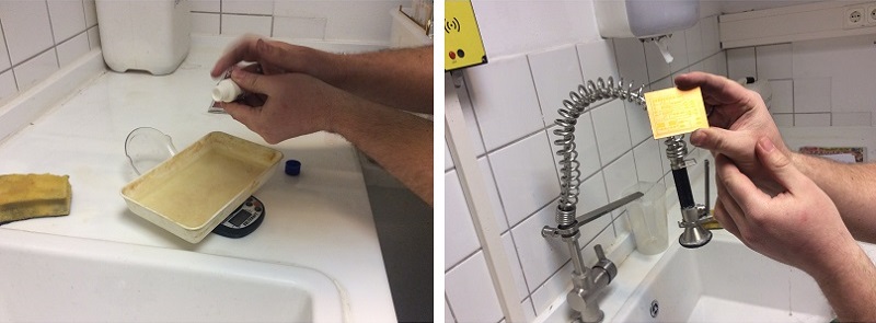
Step 5 : The plate is immersed for several seconds in a hot water bath (150mL) in which was
dissolved 2g of "revealing" which has the properties to make the lacquer soluble at the locations
affected by the ultraviolet.This step is called development.
Step 6 : The plate is rinsed under water without scrubbing (the lacquer is fragile) to remove
the rest of revealing.
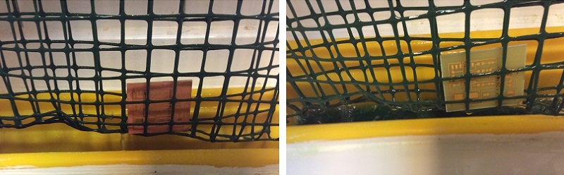
Step 7 : The plate is placed in a odium persulfate bath that will dissolve the copper surfaces
not protected by the photoresist. So we eliminated areas not corresponding to the tracks of
the circuit. This step is called etching. I let it inside during 25 minutes.
Step 8 : Abundant rinsing to stopers the action of sodium persulfate.
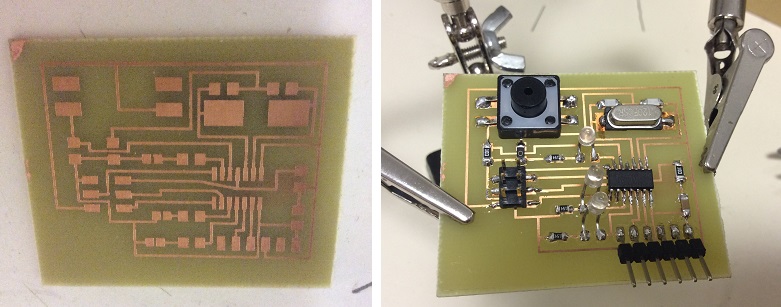
Step 9 : We re put the pcb under the UV lamps and in the revealing to remove the remaining
photoresist film on the tracks. Not too long to not remove the copper, but long enough
for the tracks are easyli solderable (10s).
Step 10 : I then had to solder my tiny components and for this I had no problem this time. May be
just one or two pads that were resistant to welding. But leaving the soldering iron on the pads
a few seconds, the remaining photosensitive layer was destroyed and I was finally able to solder
the components on it.
Software and website used