Modifing the Board
For this part I used the Eagle (Easily Applicable Graphical Layout Editor) program and the following libraries:
You can download this from this link. To load this libraries in Eagle you can type in command line use.
Creating the Circuit Schematic
Step 01.- Place all the components that you will use in the schematic window (add command). You have to edit the name (name command) and the label (label command) of all the components to avoid mistakes.
Step 02.- Connect all components following the Hello Board design (net command). You can use name commandon wires to reduce the quantity of paths, creating virtual connections between the wires with the same name.
Step 03.- Add a Button. For the button I didn't use a pull-up resistor, I connect directly to the microchip 6th leg (PA7 port), I pretend to use the internal pull-up resistor of the ATtiny44A.
Step 04.- Add a LED. I connect to the 5th leg (PB2 port) and with a limit current resistor in serie. To calculate the resistor I used the LED data sheet and the following formule (for only one LED):
| Rmin = (Vs-Vf)/I FC | Where:
|
The result is 75-Ohm to 90-Ohm resistor. I use a 100-Ohm resistor to limit the curret.
 Schematic at the end of editing (Download .sch)
 |
Creating the Board Image
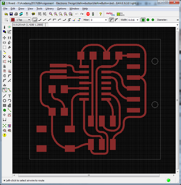
Step 01.-Go to board window (board command). Start to routing all the paths (route command), you will need some practice to do it fastly, be sure you are routing in the top layer (red). To erase path use rip command. Tip: You can use de left click to change the path type.
 Board at the end of routing (download .brd)
|
Step 02.-Edit the layers that you want to export like image (disp command). Select the top layer and the dimentions layer.
Board with Top and Dimentions Layer activated |

Step 03.-Export the board(exp command) and click
. In the window that appear, select the place to save the image or choose Clipboard, set the resolution (300-600dpi is good interval), select Full Area, and then
. After this you can edit in other program the image.
Milling and Welding
For this part I use the concepts and procedure of the Electronic Production Assignment.
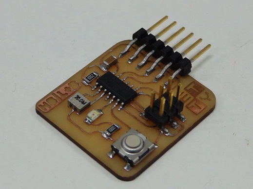
The hello Board (Led+Button) |