6. Electronics design
Group Assignment
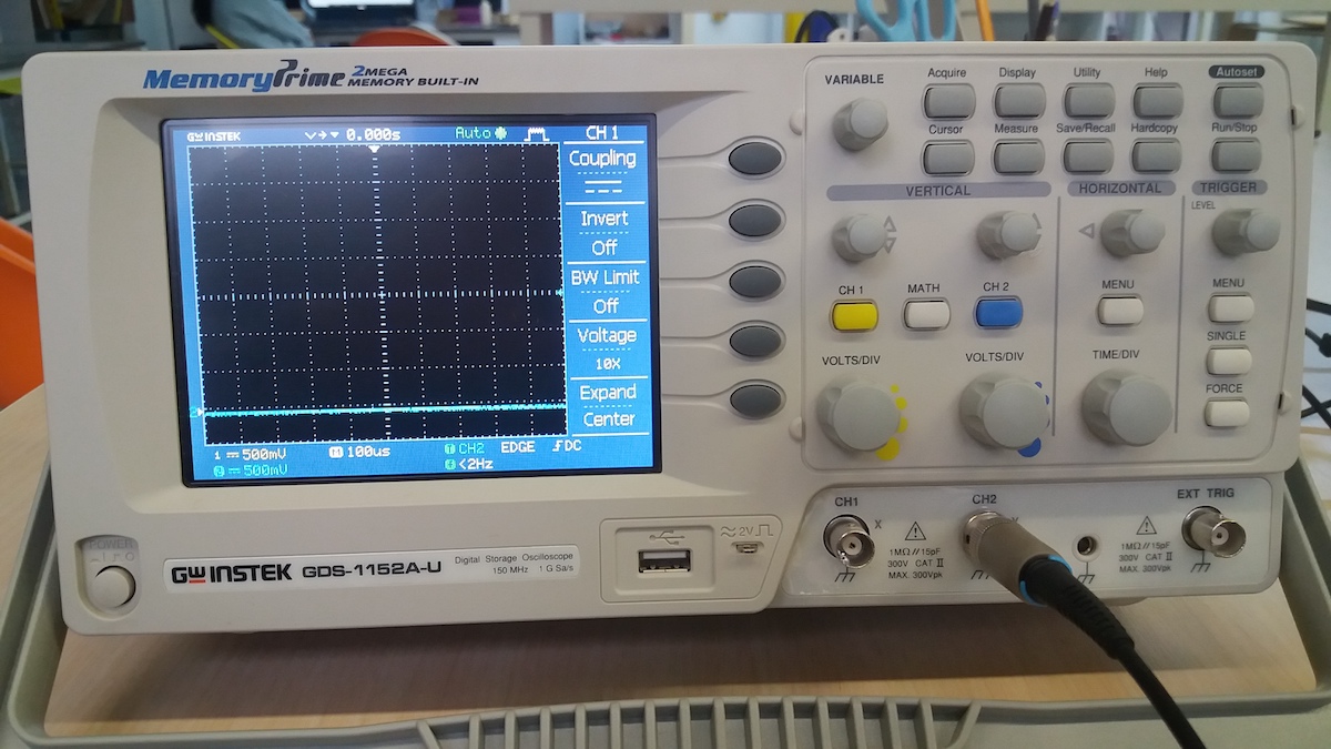
As part of a group assignment, together with our support instructor Onik Babajanyan we examined the Oscilloscope. With this instrument we can observe and measure electrical signals. Measure the frequency, noise, amplitude and duty cycles. We also learned that the magic key Autoset does most of the adjustments for us. In the past this was not the case.
The details of our group assignment can be found here.
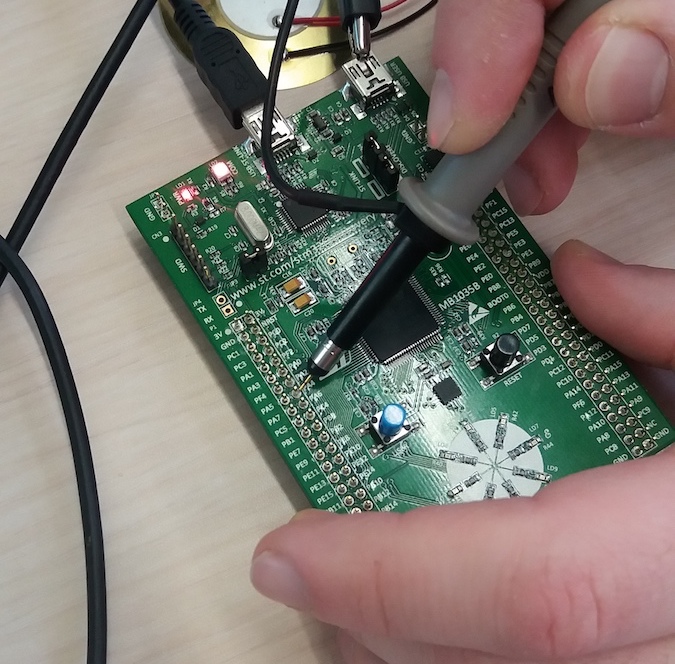
To generate signals, we choose the STM32F3-Discovery board, and programmed it in the STM32Cube IDE. The measurement was implemented by connecting one probe to the USB port’s GND and the other to the PA4 pin:
I learned about what is the difference between analog and digital signals what is a voltage ramp etc. This is a good source that explains it more.
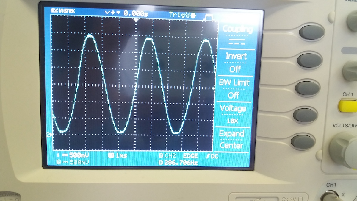
We generated an analog sinusoid signal:
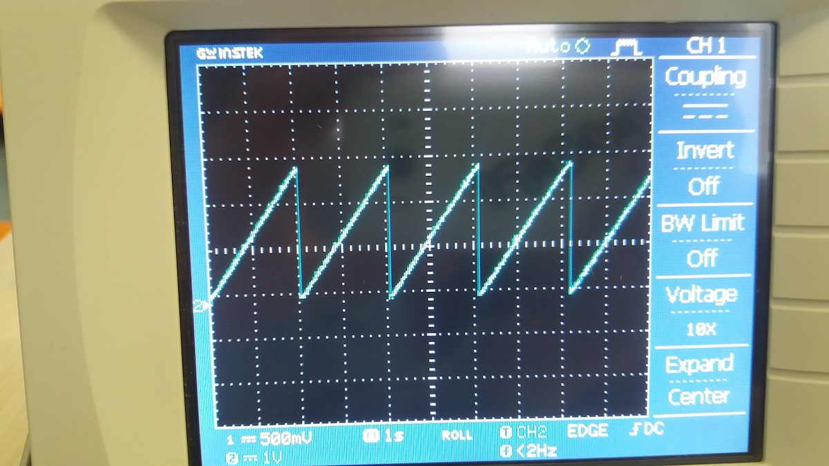
Then we generated a analog ramp signal:
Individual assignment
Within the framework of this week, a former Fab Academy student and current instructor helped me a lot to understand the structure of board design Fab Lab Armenia Dilijan Onik Babajanyan.
Install KiCad
I started working on the board design by installing KiCad, a free and open source EDA cross-platform software package designed for designing electrical circuits and printed circuit boards.
Installing the Component Library
Let’s install a component library in KiCad for components used in the Fab community. To do this, go to GitLab at the following link. There are detailed instructions on how to do this.
Schematic board design
Next, I will share with you my algorithm for designing boards, that is, where to start, what questions to answer during the design process, what the components we use need.
Let’s open KiCad and create a new project. I named my project Development-Board_SAMD11D. The program has 2 editors: Schematic Editor and PCB Editor. The rest of the tabs are for other occasions.
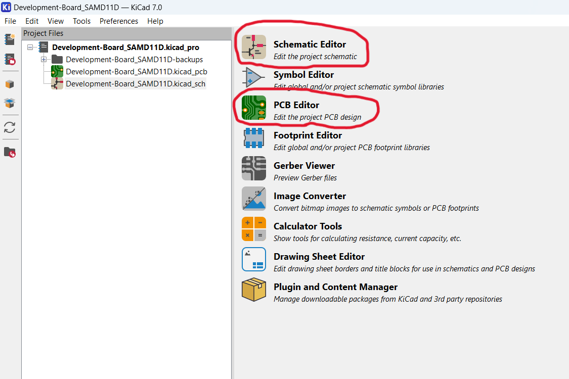
There is a very detailed documentation here, but in a nutshell, Schematic Editor helps we need to create a schematic drawing of our board, which later helps in PCB Editor to create a real board.
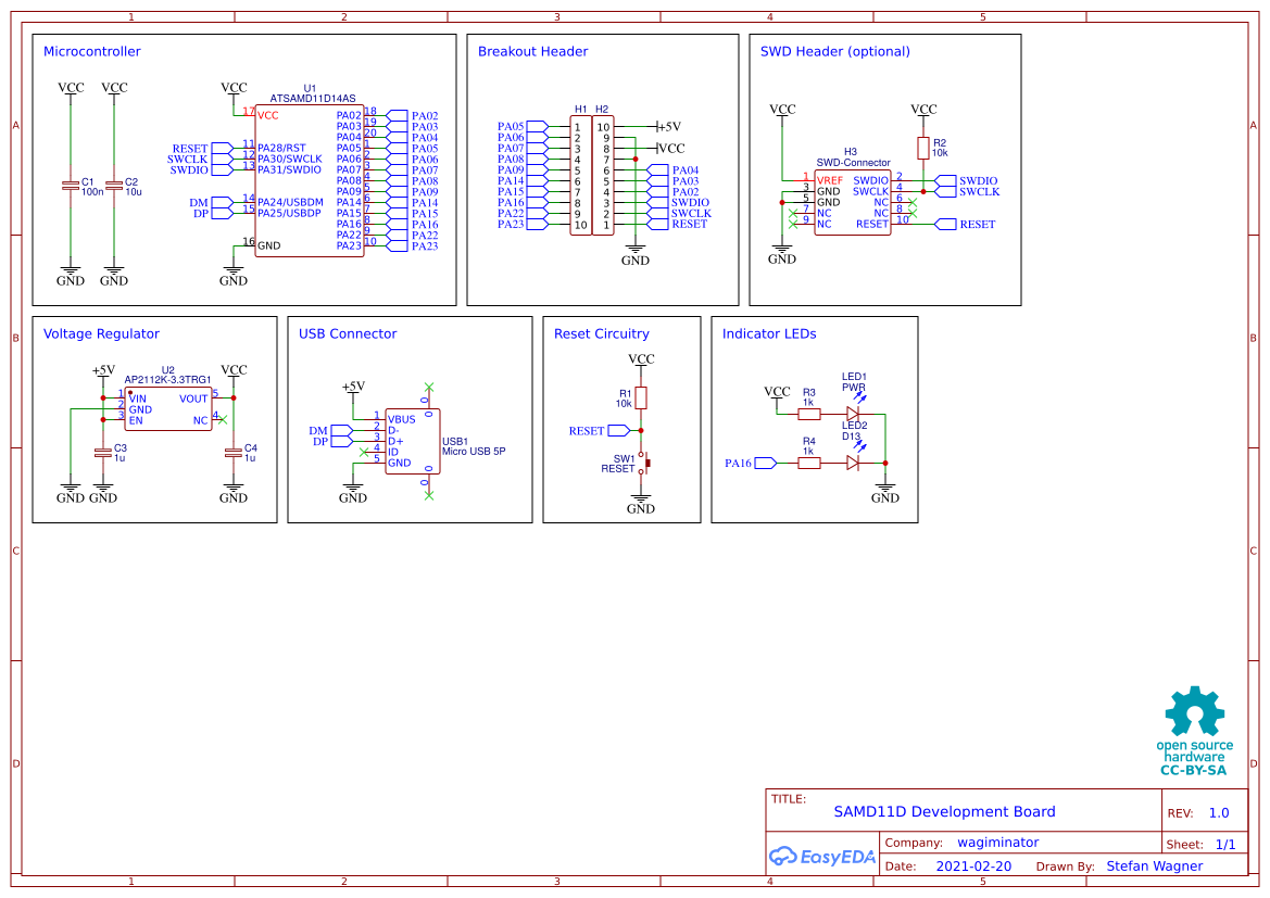
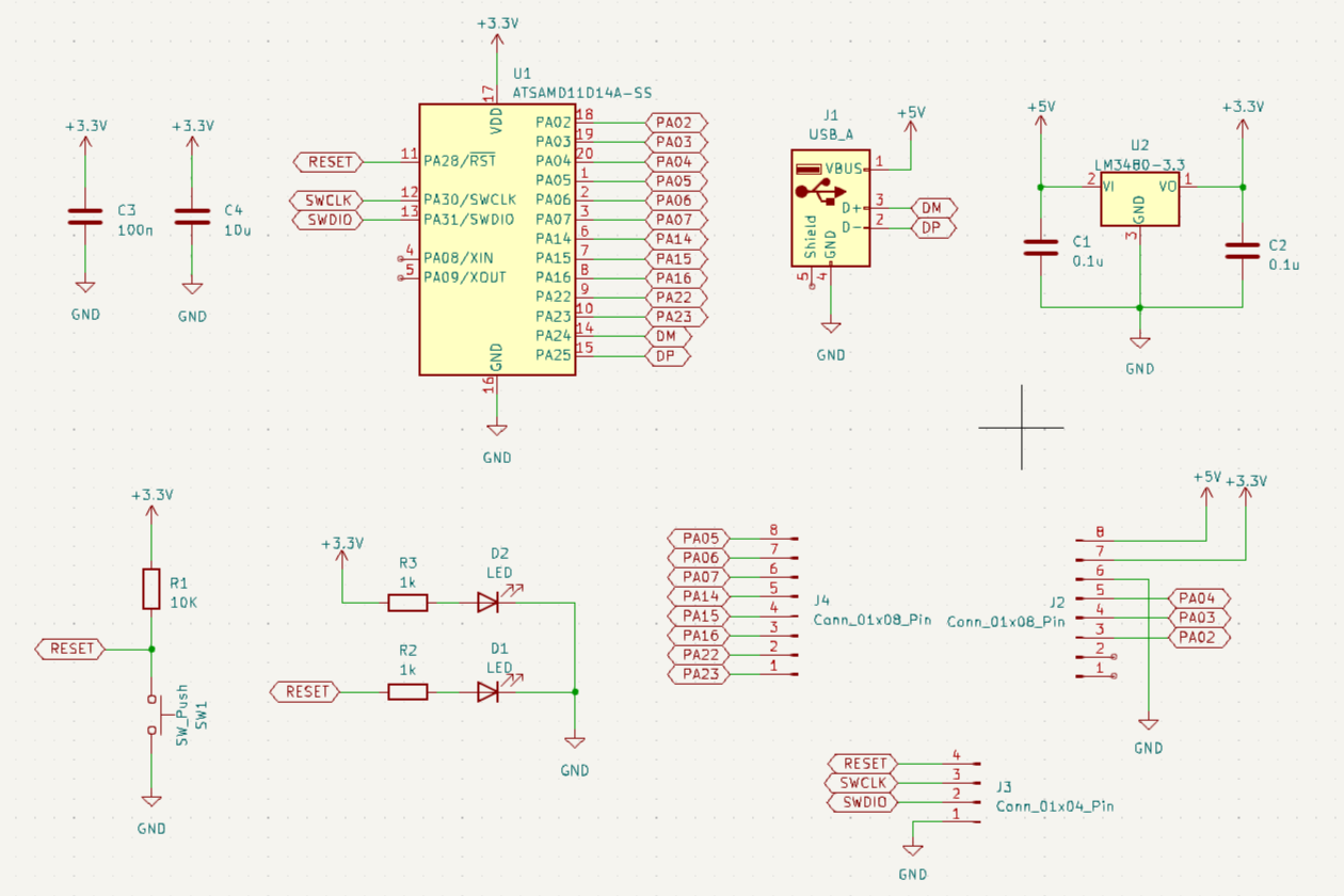
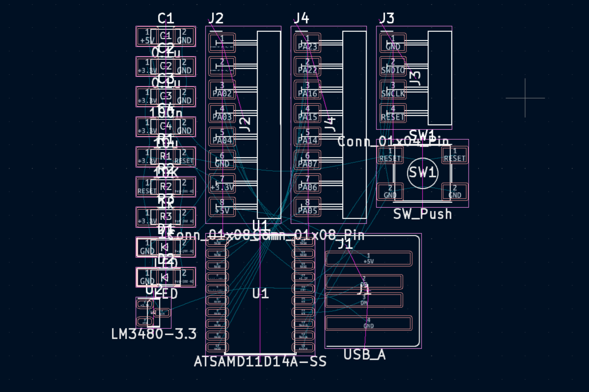
Let’s go to Schematic Editor. To design the board, I decided to use the ATSAMD11D14A-SS microcontroller, which we have in the lab.
To create a circuit board that will work on this microcontroller, there is a ready-made scheme created by Stefan Wagner. I will create my own scheme based on it.
To add its scheme, you must click on the Add a symbol button in the right menu, or simply press the A key. As a result, a list will open from which we can select the component we need.
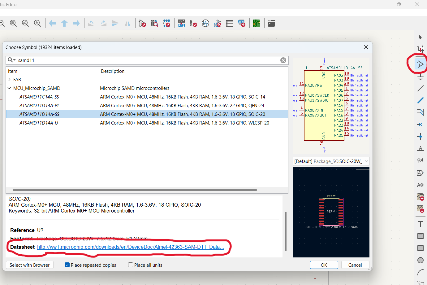
Also in this window there is a link to Datasheet of each component from the list.
When we select it and press OK, we can place it on the sheet in the place we need.
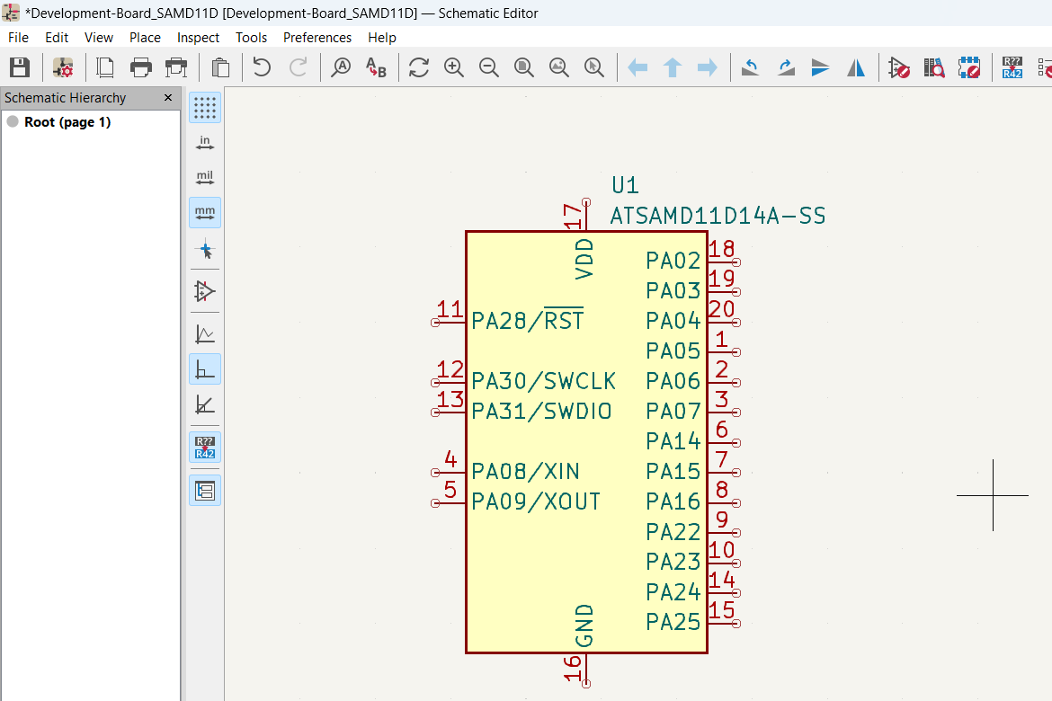
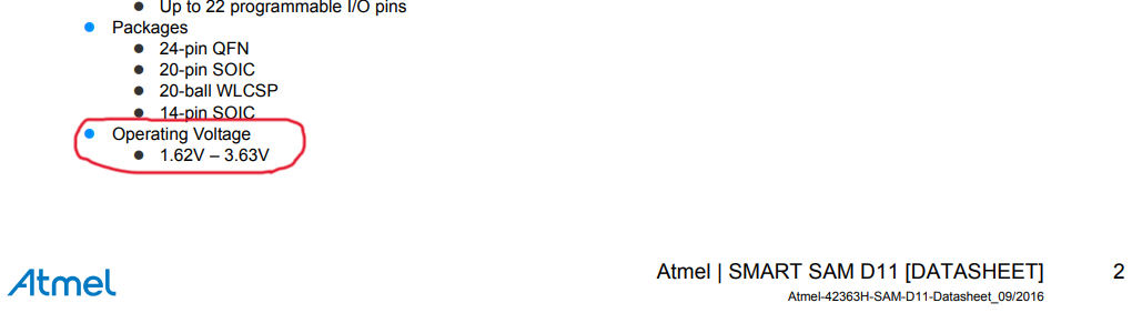
To ensure the operation of the microcontroller, the Operating Voltage *** 1.62V - 3.63V *** is required, as stated in the documentation.
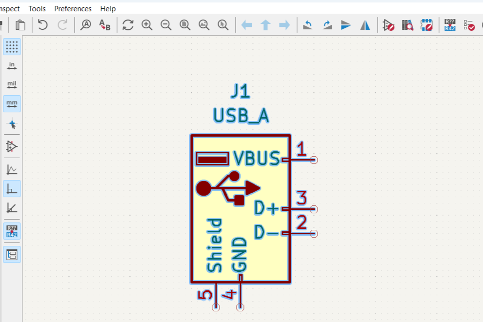
The current source for the board can be Micro USB, which provides us with a current of 5V. Let’s add it
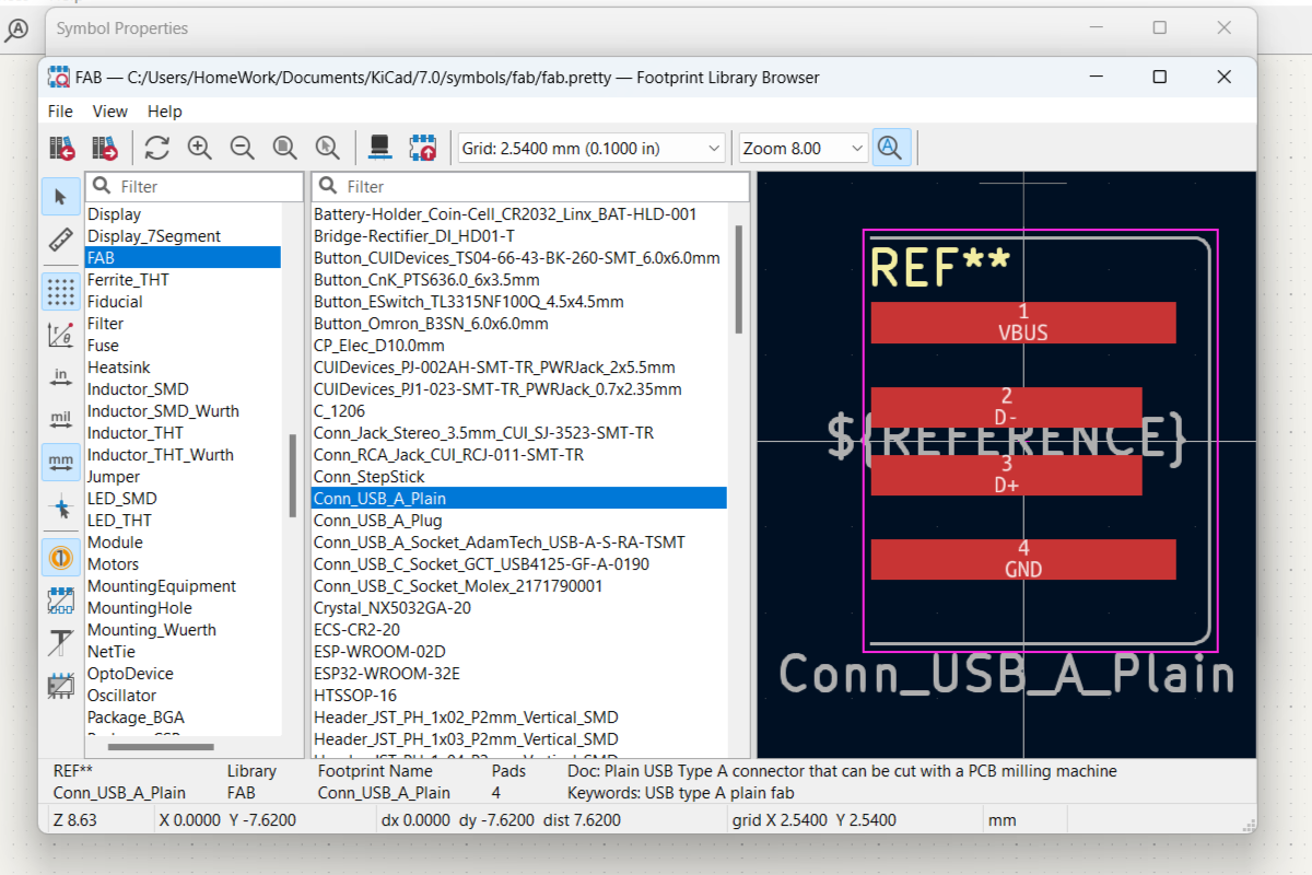
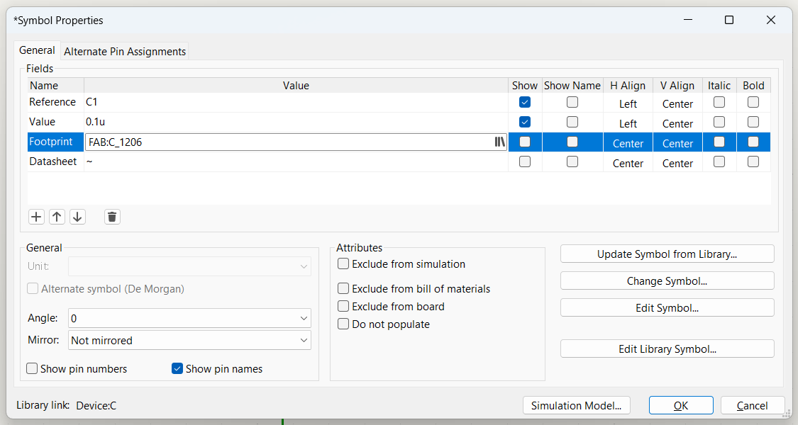
For this component, you need to specify its footprint, that is, what will be its real size directly in the chip itself. This can be done as follows: you need to select a component, right-click and select Properties, or move the button on the component and press the E key. Then click in the line Footprint in the column Value select from the list
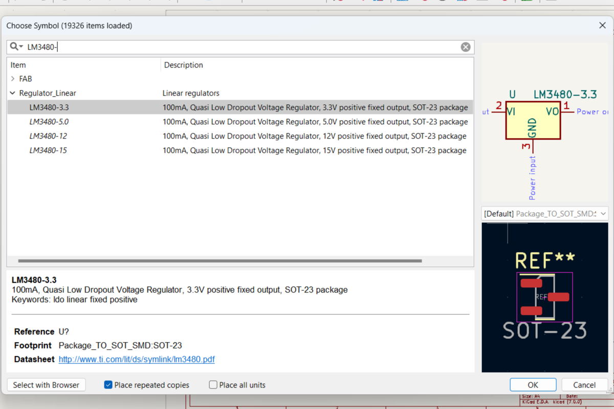
But as indicated in the documentation of the microcontroller, to ensure its operation, an operating voltage *** 1.62V - 3.63V *** is required. In order to ensure this, it is necessary to add a Voltage regulator. In my case it is LM3480-3.3.
If you look in the documentation of Voltage regulator, you can see what its circuit should be, and that for its operation it is also necessary to add two Decoupling (Bypass) capacitors.
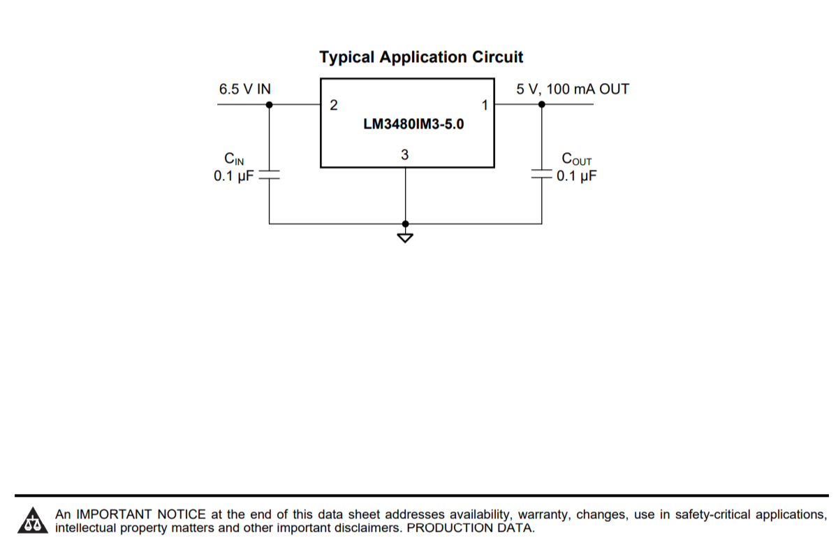
Let’s do it.
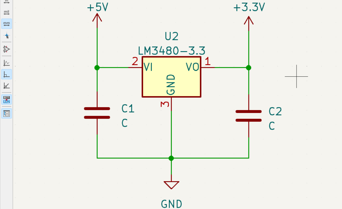
It is also necessary to write down the capacitances of the capacitors and their Footprint.
In addition to the method of connecting contacts to each other using the wire tool, there is another way that is done using the global label.
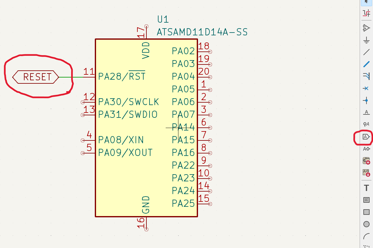
This method is good because the circuit is not confusing, we can draw some blocks of the circuit separately, and if we assign the same global label to two contacts of different components, then the program will understand that these contacts must be interconnected. To do this, let’s draw a block diagram in which there will be a RESET button.
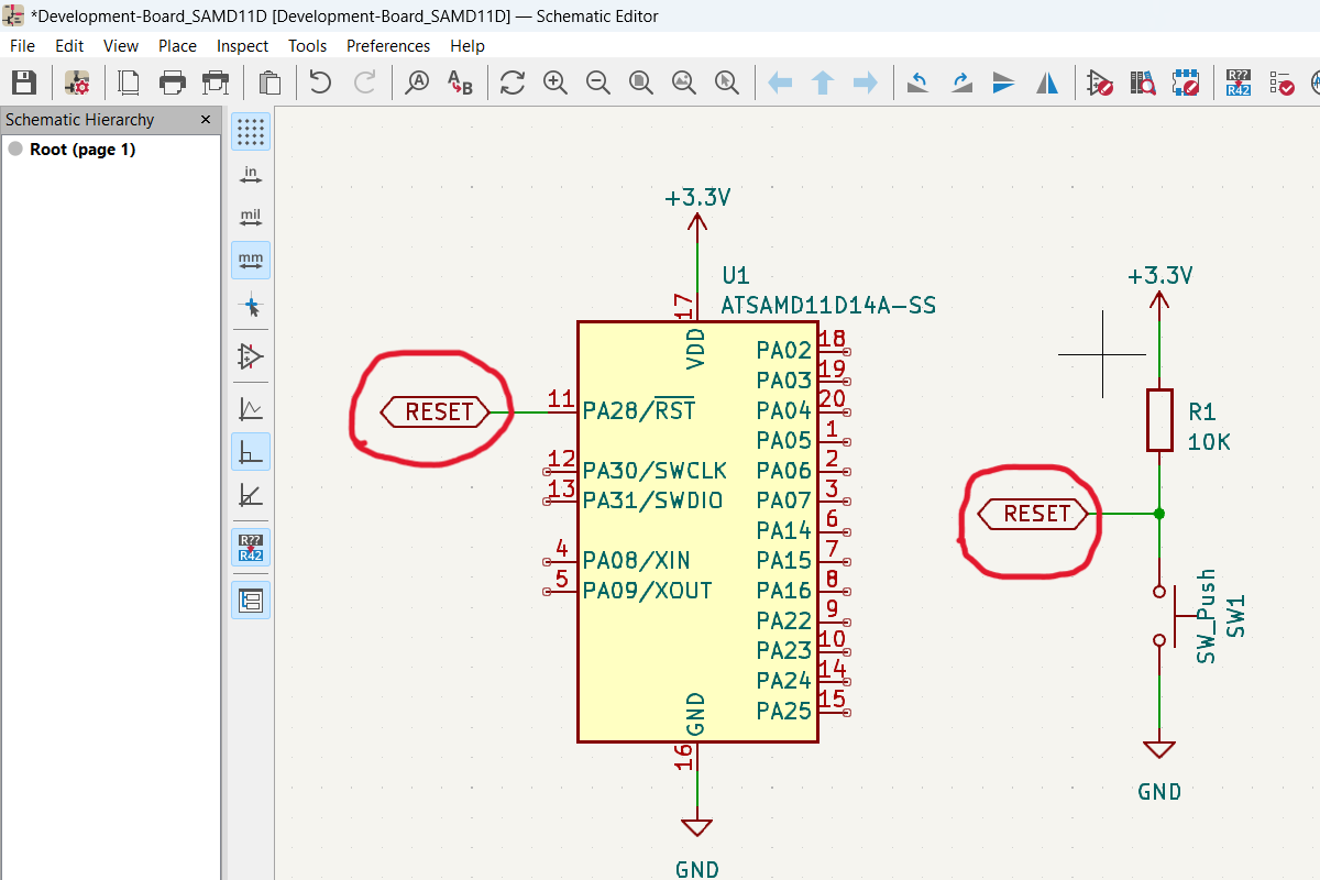
In this case, the program will understand that they are connected to each other
Also, let’s create a block diagram where when the board is connected to the power supply, the LED will light up in it, and also, so that when you press the *** RESET *** button, another LED will light up.The LEDs will be powered by a voltage of 3.3V. But if you look in the documentation of SMD1206 LEDs, you can see that the recommended voltage for the LED to work is 2V.
Based on the fact that the supplied voltage is 3.3V, and the desired voltage for the LED is 2V, then it becomes necessary to connect a series-connected current-limiting resistor. In this scenario, the scheme will be as follows:
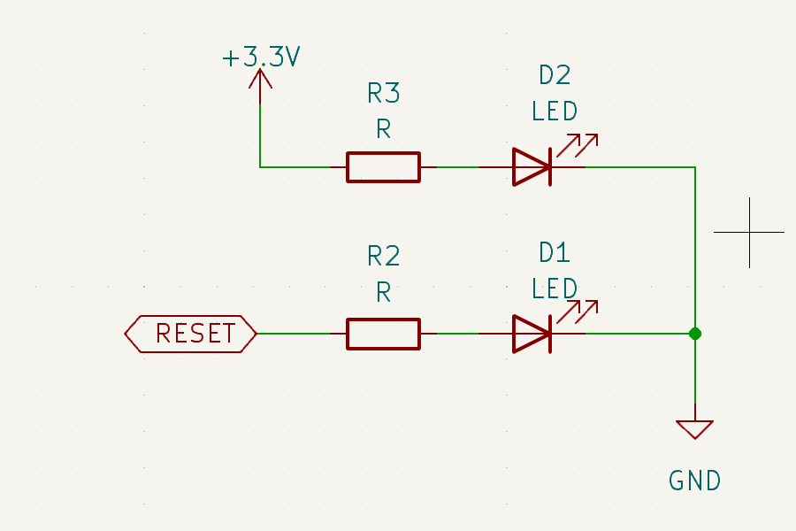
If you look at the Stefan Wagner schematic you can see that the current limiting resistors supplied are 1 kOhm . Let’s put it in the program:
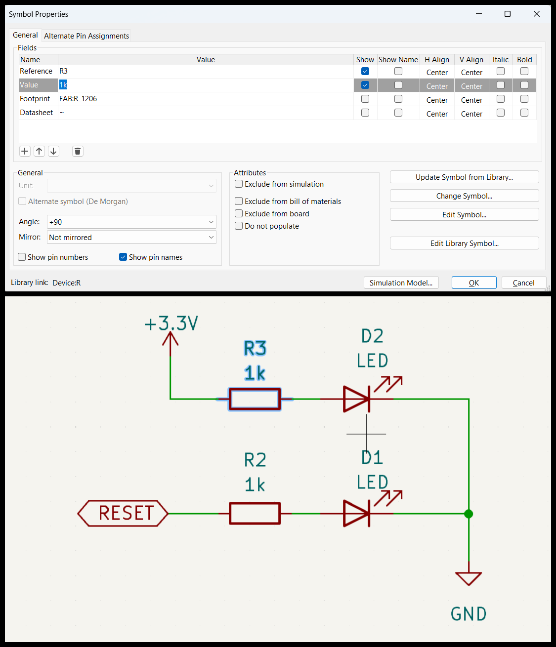
Let’s see how the resistance of a resistor is calculated. The applied voltage is 3.3V, and we learned from the LED documentation that the desired voltage drop for it to work is 2V. Since the current-limiting resistor is connected in series, it follows from the law of series connection of circuits that when connected in series, the total voltage in the circuit is equal to the sum of the voltages on the individual elements. The voltage drop across the current limiting resistor will be:
U = 3.3V - 2V = 1.3V.
The LED documentation indicates the desired current strength of 20 mA. Since the current in series connection is the same in any part of the circuit, the current through the resistor will also be:
I = 20 mA = 0.02 A.
U = RI
Let’s calculate the required resistance of the resistor based on Ohm’s law:
R = U / I = 1.3 / 0.02 = 65 Ohm
So, to achieve the desired current of 0.02A (20mA) with a voltage of 3.3V, you need to connect a current-limiting resistor with a value of 65 Ohms in series with the LED.
But close to the value of 65 Ohms in our laboratory is a 100 Ohms resistor. Using a larger current-limiting resistor may cause the LED to dim.
I won’t change the value in the scheme for now, as I don’t need the LED to be too bright. After cutting the board and soldering all the components, if the LED is too dim, then I will change it.
Let’s also draw some connectors. As you can see the use of labels makes it easy to follow the schematics and helps to avoid wires going all around and creating a mess.
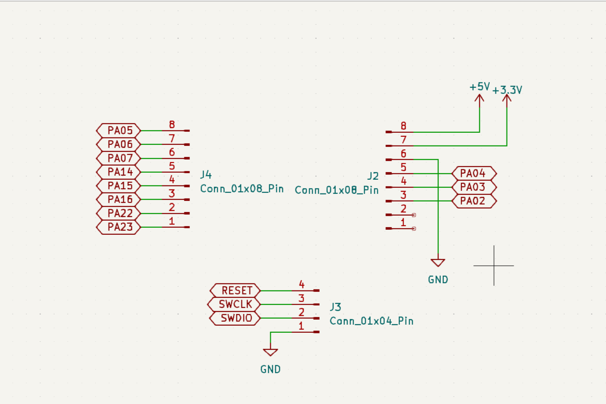
The final diagram will look like this: Another point that I learned and want to highlight is that it’s better to keep all power inputs on the top of the schematics and ground connections or GND at the bottom. This also helps to better organize the schematics.
But before moving on to the PCB Editor, we need to make sure that all components have their Footprint set. This can be done by going to Tools -> Assingn Footprints. The footfrint library has many different packages of the same component. The package we use at fablabs is 1206 for capacitors, resistors, LEDs etc.
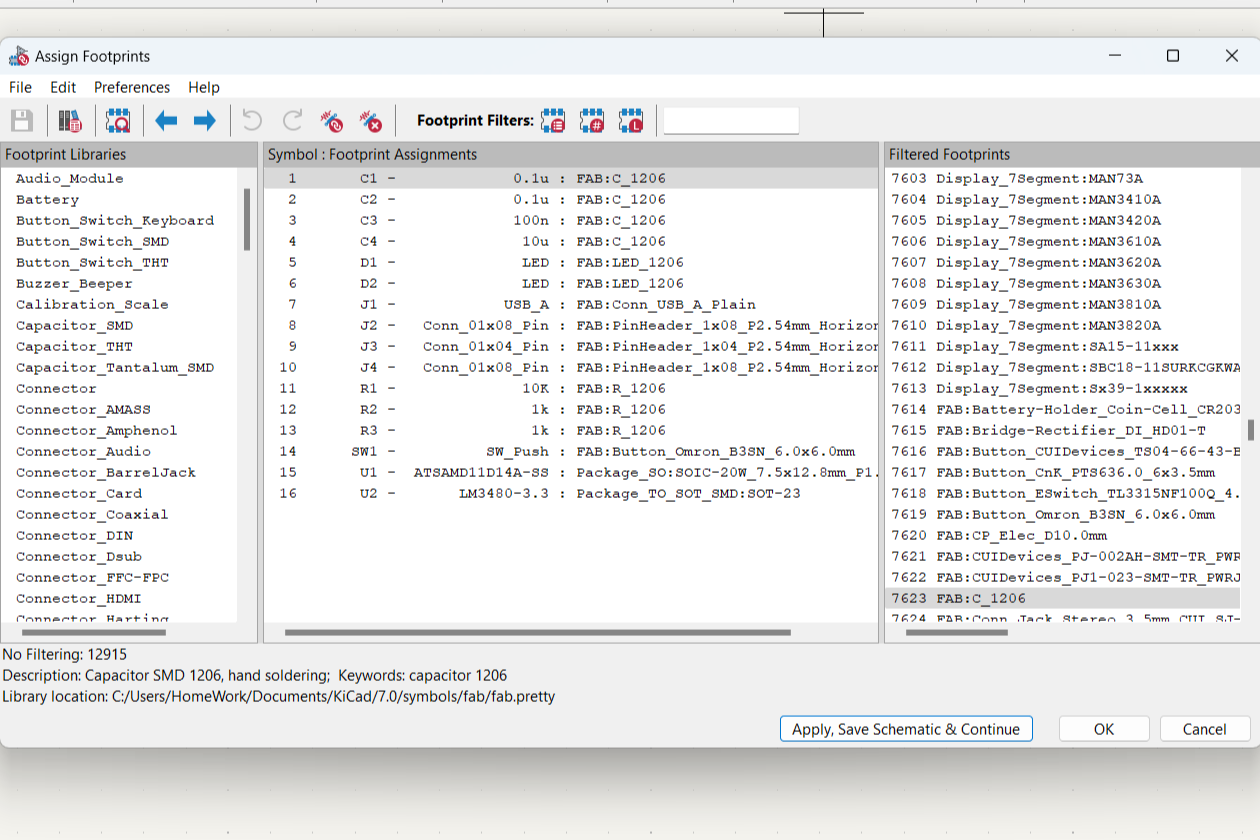
If all footprints are set, then you can already go to the next step.
PCB design
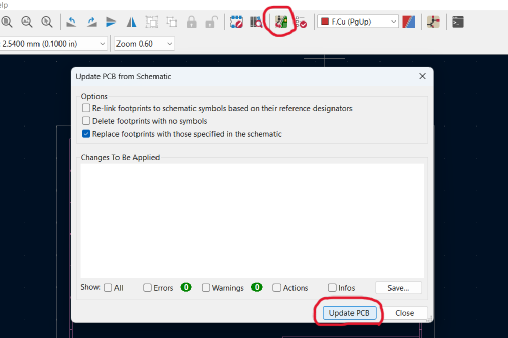
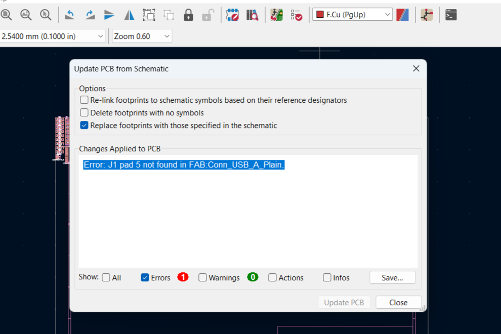
You need to go to PCB Editor and click on Update PCB with changes made to schematic (F8). Then check Replace footprints with those specified in the schematic and click on the Update PCB button.
In my case, one error is generated, which can be ignored, we do not need it.
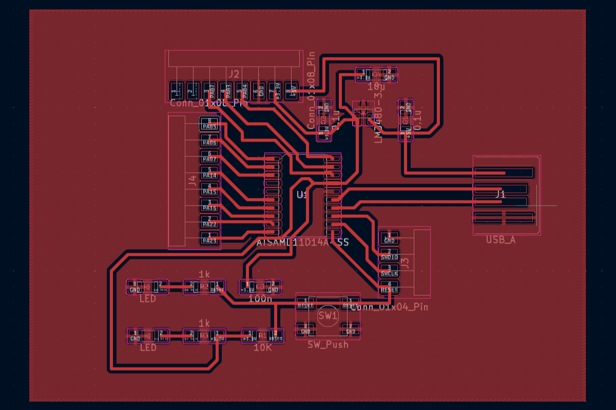
As a result, the actual sizes of our components were generated, which are connected by green lines depending on our schema.
These green lines are auxiliary lines. Oriented by them, we must connect our components with paths.
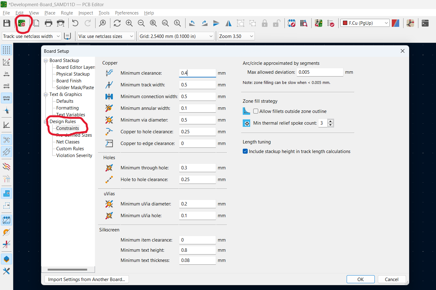
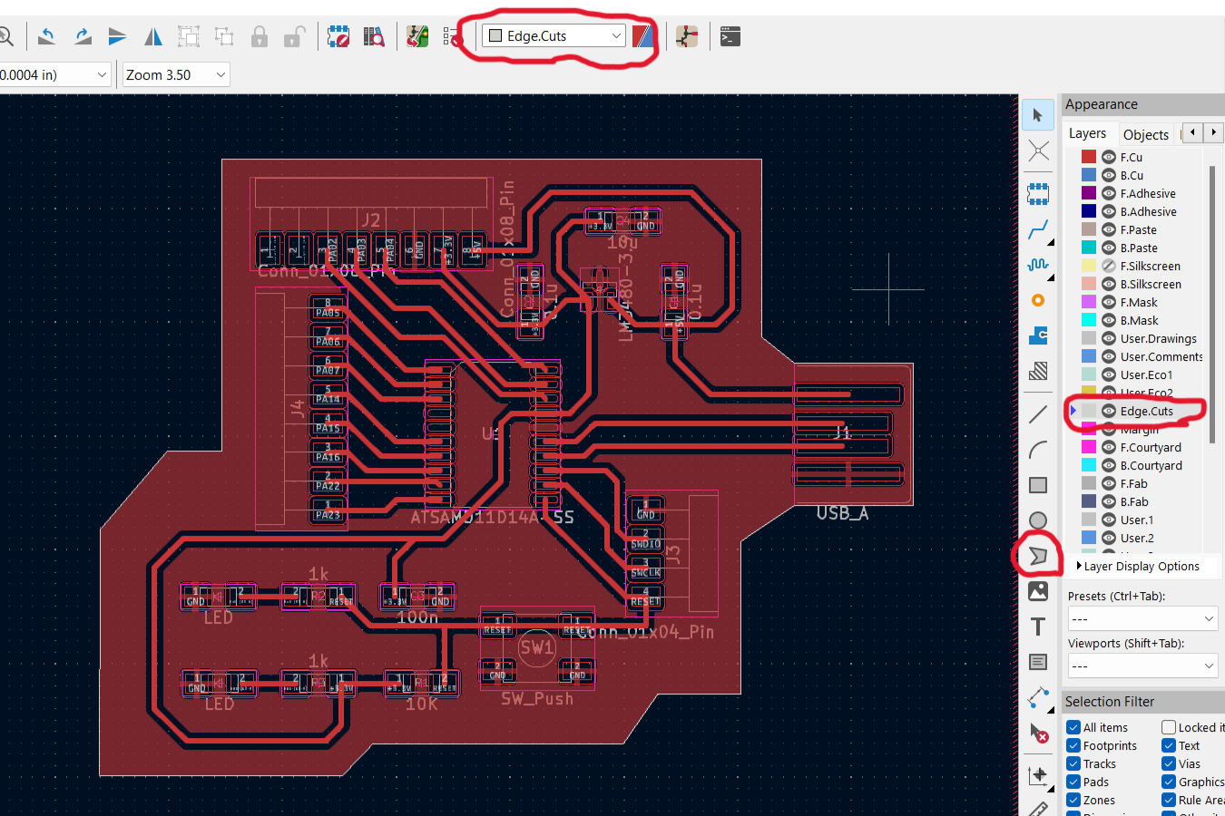
In order not to change anything in the future, you can first set some configurations: minimum clearance (minimum clearance), minimum track width (minimum track width), minimum connection width (minimum connection width), etc. These dimensions are also related to the fact that the minimum diameter of the cutter that we will use is 1/64 inc = 0.396748 mm. To enter these settings, you need to go to Edit board setting including layers, design rules and various defaults –> Design Rules –> Constraints
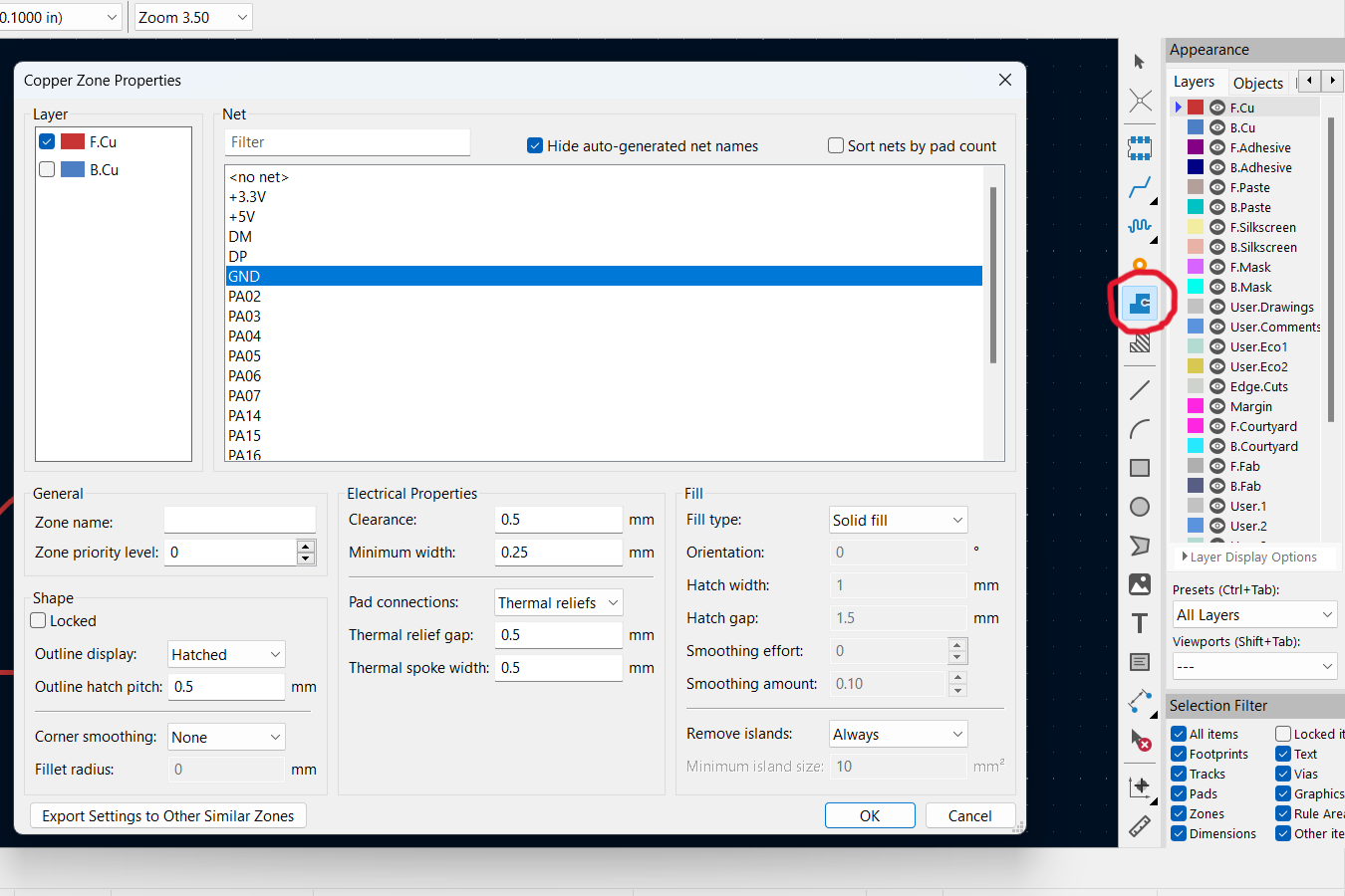
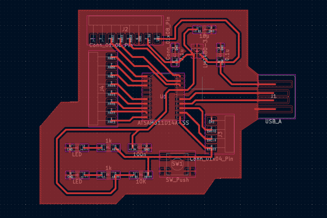
All components are in scattered order. Let’s place them more conveniently so that we can connect the corresponding component legs to each other. Those places where the cutter should not engrave can be used as GDN. To set this, you need to use the Add a filled zone tool. You must select GND and set the contour.
The process of placing the components took me a lot of time, but in the end I managed to set all the necessary connections.
I drew a GND area of such a size that it contained all the components, this area can later be replaced by another area.
In theory, the outline of the board can be drawn in another program and exported to KiCad. In my case, it is important to observe the width and length of the USB, which are respectively 10.5mm and 12.5mm.
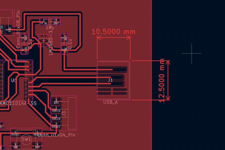
While I don’t make a special design for the board, I will follow its necessary contour and see what happens. To build the contour, I used the Draw a graphic polygon tool and made the construction on the Edge.Cuts layer. And here’s what happened:
If left in this way, then at the moment when the board enters the USB port, a short circuit will occur, since all contacts will touch the GDN.
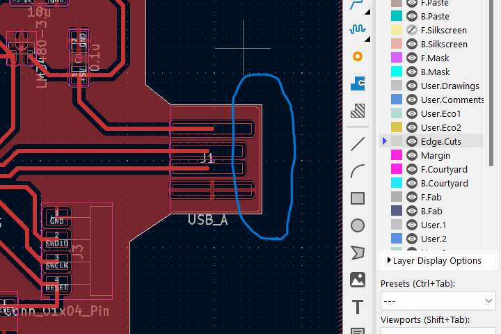
For this reason, I will delete the GND layer and draw a new GND layer along the board outline so that it does not touch the USB part and this will be my final result.
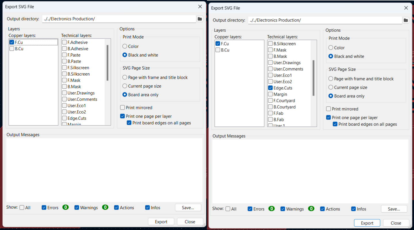
Export SVG files ready for production
In order to generate G-code we need to export our layout in SVG format. To cut the board, we need to export two files: one for milling tracks and the other for milling a contour.
Conclusion
This week has been very interesting for me. While working at FabLab Armenia Dilijan, I had seen various boards and components, but the whole picture did not add up for me. This week has helped me to understand how the design of the board is done and what are the common variables in the process like thickness of tracks, footprint sizes, component packages, number of layers etc, and in particular one thought helped me a lot: the microcontroller plays a leading role on the board and other components are added based on what is necessary to ensure microcontroller’s operation for example we add a 100nf or 0.1uf capacitor to the power pin to filter out noises coming from power supply.