Week 04
Electronics Productions
Group assignment Characterize the design rules for your PCB production process: document feeds, speeds, plunge rate, depth of cut (traces and outline) and tooling. document your work (in a group or individually) Individual assignment Make an in-circuit programmer by milling and stuffing the PCB, test it, then optionally try other PCB fabrication process.
Group assignment
 - Characterize the design rules for your PCB production process: document feeds, speeds, plunge rate, depth of cut (traces and outline) and tooling.document your work (in a group or individually)
 - Practice and merge info into a way of using the milling machine
 - look at fabstudents before us
 - understand the milling procedure
We decided to have a set up with one person (me) behind the computer in the Waag that controls the milling machine and another one (paula) at the same time running mods on her own laptop to be able to have more screen space (and screensaves) and feed of each others input.
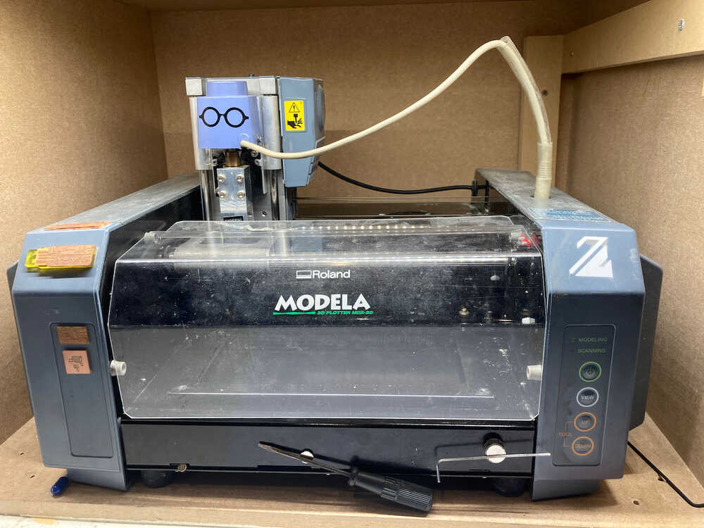
Machine@deWaag is a Roland Modela MDX mill on, the machine has an accuracy of 0.002mm in theory, the machnical parts (end mill) will made this number rise a bit but the theory sounds great.
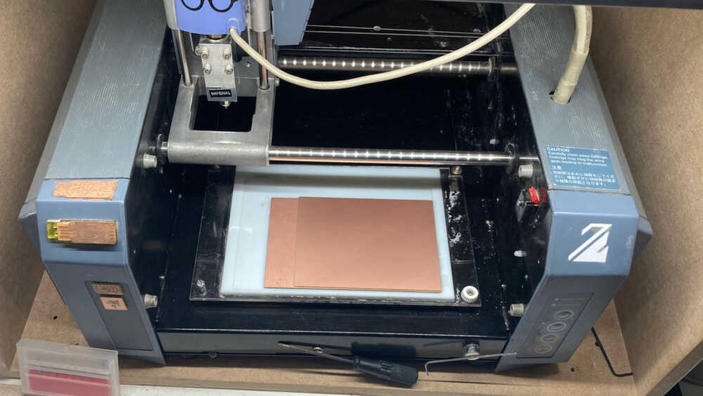
Start with setting up the plate, which Henk did for us this time. the most importing thing to keep in mind that it should be as clean and flat as possible, so make sure you take off all the old tape and put the new one on the whole plate nice and flat, don’t forget to press it on.
There are 3 plates:
- bottom/base plate which is attached with screw to the machine
- the actual plate that we are gonna cut from
- in between those the sacrificial layer, that can be damaged but since its copper it will not wear the mill out.
In terminal we typing in mods to connect the computer to the machine.
mods

Milling:
-
Open
MODSin the browser, right click, program, Roland MDX mill, PCD -
Go to
WebSocketSerialclose both port/socket and open them again, just to work around a little bug at the Waag.
-
upload traces file, which we found here
read PNG
-
Check DPI - minimum 1000 to avoid inaccurate traces
-
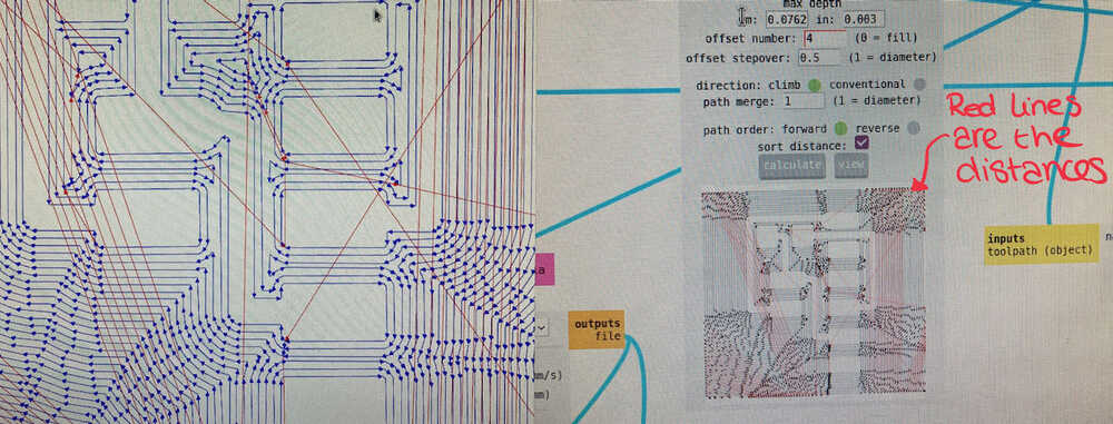
Go to PCB window press
mill tracesthis feeds the Mill Raster 2D window -
in Mill Raster 2D fill in the tool
diameter:0.4mmand the cut depth:0.003inchesCare full with the inches/mm and change themax cut depth:0.003inchessame as the depth since we are making traces. -
press
calculate(translated to Roland his Gcode which is RML) andviewthis opens another tab with a 2D view -
check
offset: 4(offset means the amount of lines he tried to put in there, if it doesn’t fit he goes 3, 2, or even just one time), but if youoffset:0it will take away all the excess copper and just leave the traces.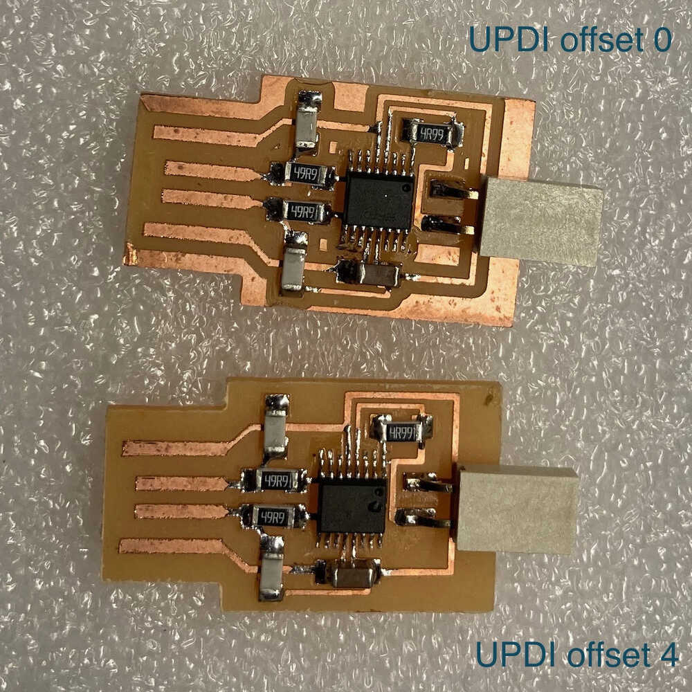
-
offset step over: 0.5this means it will start the next line only half the diameter further, this is to avoid bumps in the traces. -
then there is also
path orderwhich seems arbitrary, probably useful for real PCB creators andDirectionwhich has everything to do with how the flute (wings) of the mill chop copper off, either down or up towards the travel path. Henk tried to explain but honestly its hard to put in words.. some explanation i found online helped me to understand and i made this drawing to visualize it.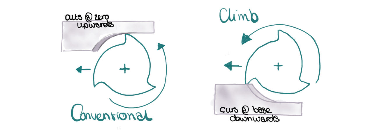 The copied text from Harvey Tool:
Climb milling is generally the best way to machine parts today since it reduces the load from the cutting edge, leaves a better surface finish, and improves tool life. During conventional milling, the cutter tends to dig into the workpiece and may cause the part to be cut out of tolerance.
The copied text from Harvey Tool:
Climb milling is generally the best way to machine parts today since it reduces the load from the cutting edge, leaves a better surface finish, and improves tool life. During conventional milling, the cutter tends to dig into the workpiece and may cause the part to be cut out of tolerance. -
in 3D tollpath viewer click
viewto open a new tab with the 3D traces, check if the design makes sense.
-
go to the Roland MDX/iModela window
cutspeed:1otherwise you will break the tiny 0.04mill -
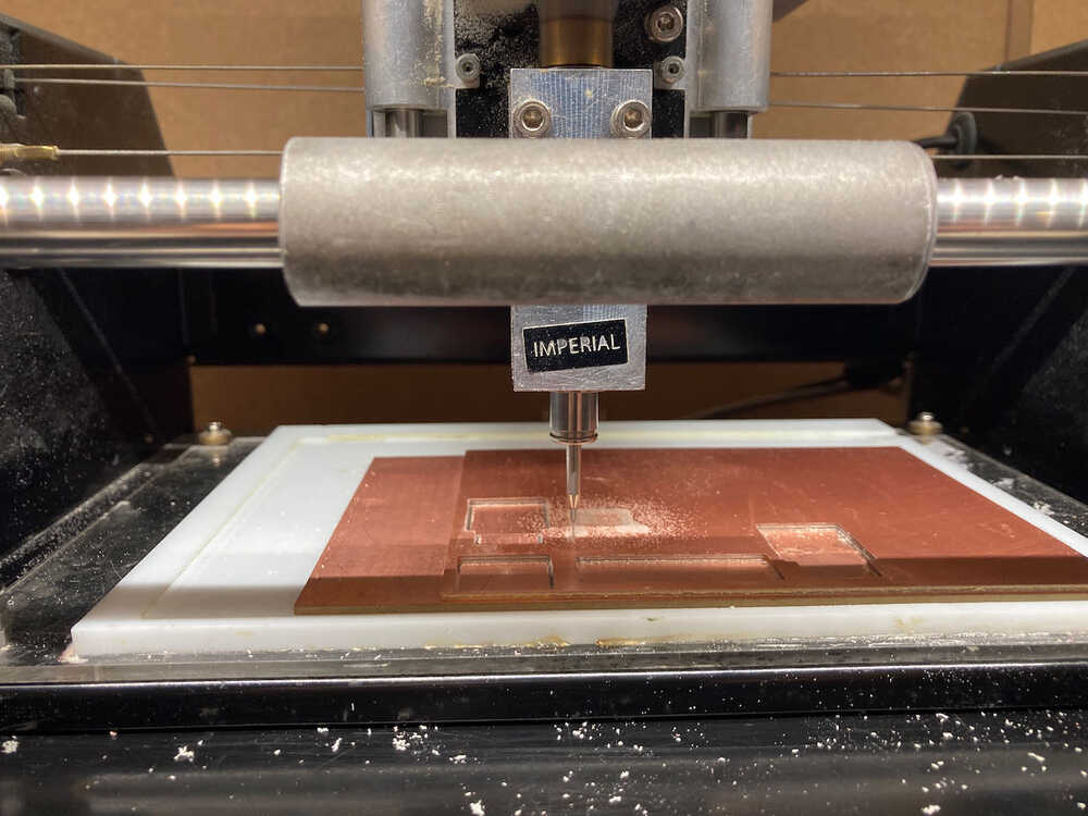
now its time to put the mill in a controlled and zen way
On the Roland press view twice to move the plate and mill to a workable position, lower the mill a bit with DOWN not to low you still have to be able to take the mill out. With the allan key open the lock (marked blue) while holding the drill so it doesn’t drop and breaks. Place it in the little box (on the left where the good ones are) and get the 0.8 mill from the magnet on the front, place it in as deep as possible for stability. Tight the screw gently, not to strong.
make sure the mill is high enough (above the plate) to continue with the software
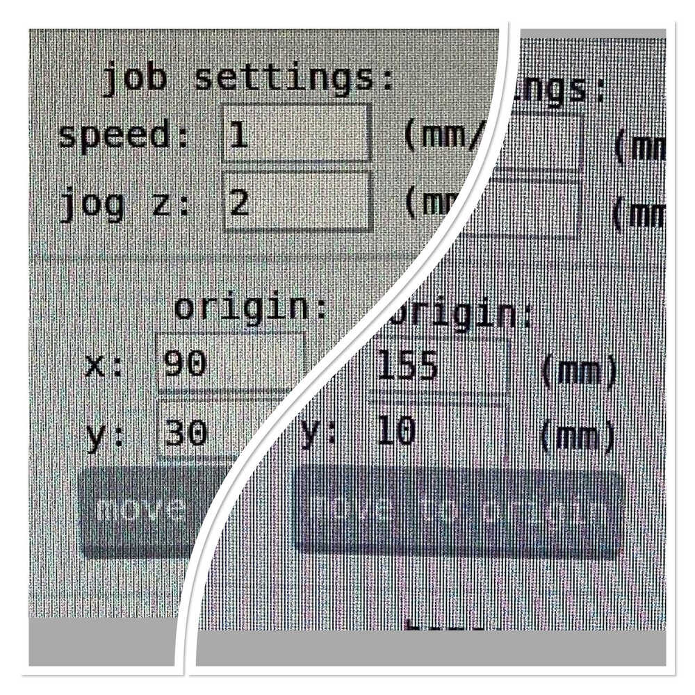
- in the Roland MDX/iModela window move the origin to the desired place (check the origin base lower with the dots) in our case
origin x:70 y:6Tip from Henk: take a picture just in case - press
move to origin
Unscrew the mill while holding it to lower the mill on to the plate, tap it gently to make sure it is on the plate and lighty tightly again the screw.
- just to be sure we would
calculateit again - press
send file
when its finished we took the vacuum cleaner to remove the dust, making sure we don’t move the plate (which should be impossible anyways) and continue to cut the outline
The process is very similar to the traces one only less to alternate in the inputs.
-
start with the upload of the interiour file, which we found here
read PNG -
check DPI - minimum 1000 to avoid inaccuracy
-
go to PCB window press
mill outlinethis feeds the Mill Raster 2D window -
in Mill Raster 2D fill in the tool
diameter:0.8mmand the cut depth automatically changes to :0.6096 mm -
change the
max cut depth:1.6mmto make sure it cuts through but not in the sacrificial layer -
press
calculateandviewthis opens another tab with a 2D view -
set
offset: 1and `offset step over: 0.5' -
in 3D toll path viewer click
viewto open a new tab with the 3D traces, check if the offset is right. -
go to the Roland MDX/iModela window
cut speed:4since we are gonna change to the 0.8mill -
now its time to put the mill in a controlled and zen away
make sure the mill is high enough to continue with the software
- in the Roland MDX/iModela window check the
origin x:70 y:6should be still there from the traces - press
move to origin - just to be sure we would
calculateit again - press
send file
Our cut out didn’t need much sanding with paper, already very smooth but washing with hand soap was our last group effort before we all went our own way
picture of the group
Soldering
First rule is stay zen and organized
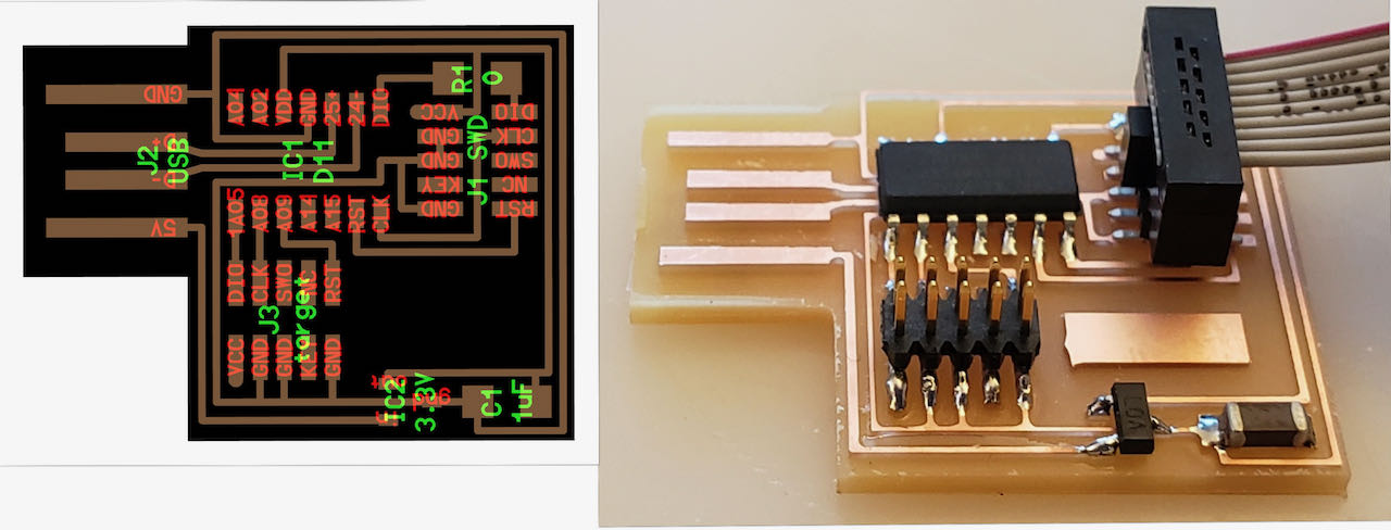
When you look at the drawing and picture of the board you can see what you need to collect.
One box at the time to avoid a mess and misplaced parts.
Here you see Henk soldering a UDPI, rules of soldering seems simple in theory.
- heat up the place with the 340º solderiron
- add solder
- take away the solder
- move iron away
If you need to there is always the sucker, which can be use with mistakes but also on purpose when you have put solder on all the legs of a ATtiny and you need to take away the excess to avoid shortcircuit.
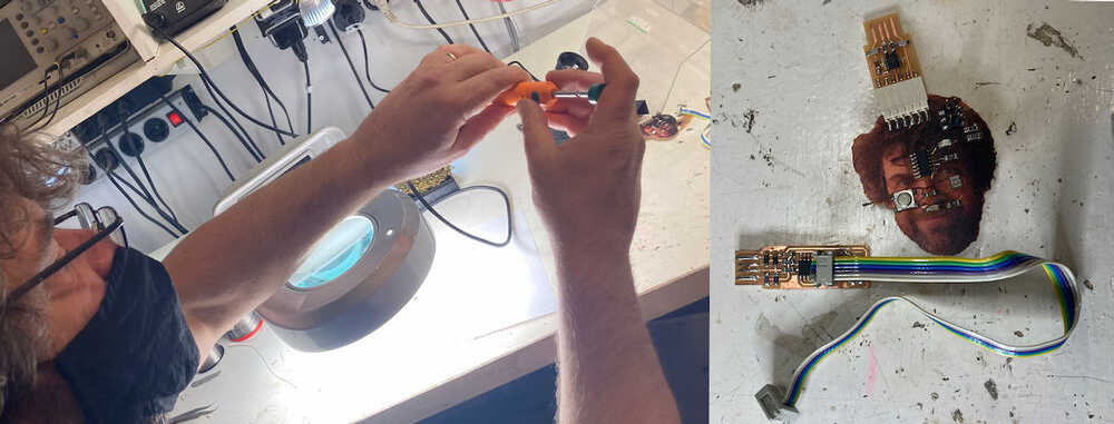
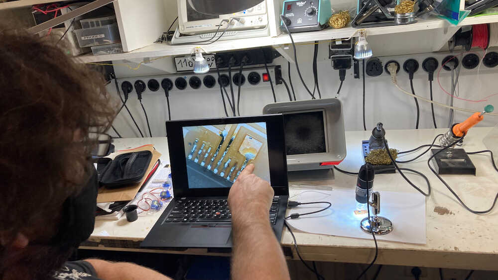
At the Waag there is a small camera where you can check the pcd close up with.
individual assignment
- Make an in-circuit programmer by milling and stuffing the PCB, test it, then optionally try other PCB fabrication process.
- stay calm and zen and learn proper soldering instead of the baking that i normally do
- look at a few tutorials before holding a solder iron
- finish the JTag and make a UDPI (hopefully also understand the difference)
Making our own pcd:
Since we were running out of time, Lucia and myself decided to join forces to make have it finished by the end of the day. Both doing our own milling but instead of changing the plate in between, milling 2 traces first then change the mill to cut the outlines. We wanted to try another pcb then the ones before us so we choose from the option that Henk provided a Hello JTag board, which appears to have to be programmed after we make it, challenge coming up.

Here is the mods settings we went through, of course basicly the same except for the file names and origin.
So we both had our own origin si we could both do the traces and only then change the mill, but while changing to mine without tapping the mill again we realized that was a very bad idea, apparently the plate was a bit round because of all the cut outs already so it was cutting half the traces.
always tap on origin again
We had 2 choices wait till it was finished or cancel, we choose the last option with help from Henk. First of all you hit the cancel in Mods and then on the machine if i remember correctly it was:
- up/down together till the view started blinking after about 10sec
then it was a matter of tapping it on the origin and start again with the traces, thanks Henk for staying a bit longer so we could finish also the outlines which are called interior for some mysterious reason.
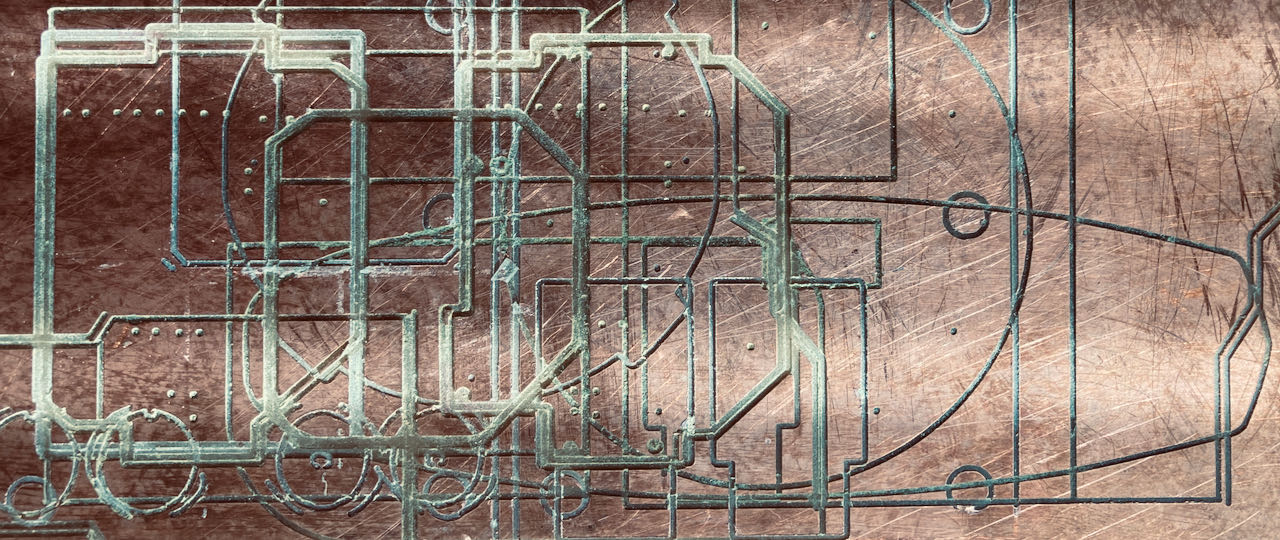
These are some of the air travel lines which i think looked so good.
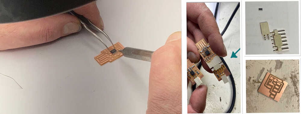
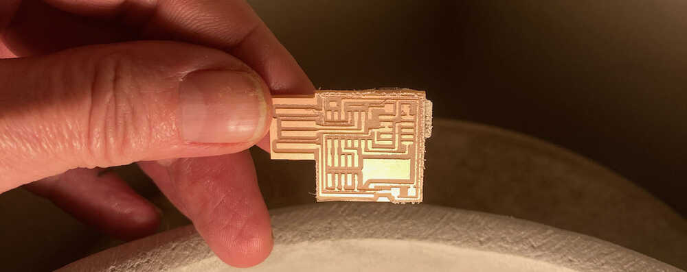
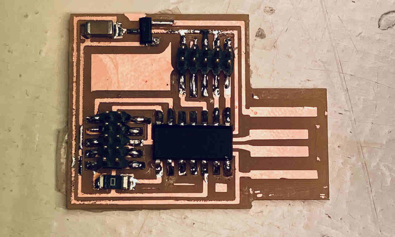
My JTag fresh out of the machine, no i need to figure out if i should take away the excess copper.
Soldering my own JTag
And yes i had to clean the excess copper of my board to avoid short circuit, with a stanley mes it only took me 5 minutes to do this. After that i gave it a nice clean up so i was ready to solder.
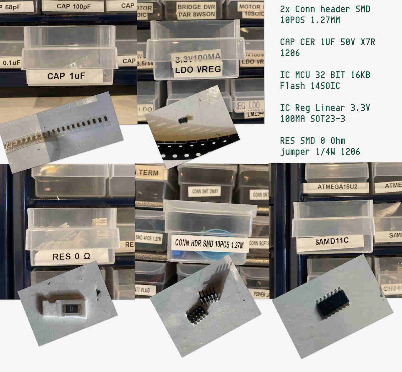
Then components time, it was a bit of a search for me to match the names that are on the board drawing to the components in the Waag but with the help from a list that i found in Daniel Meyer documentation i was able to connect the dots. Made this little drawing on top of the PNG from the fabsite for myself to understand a bit better.
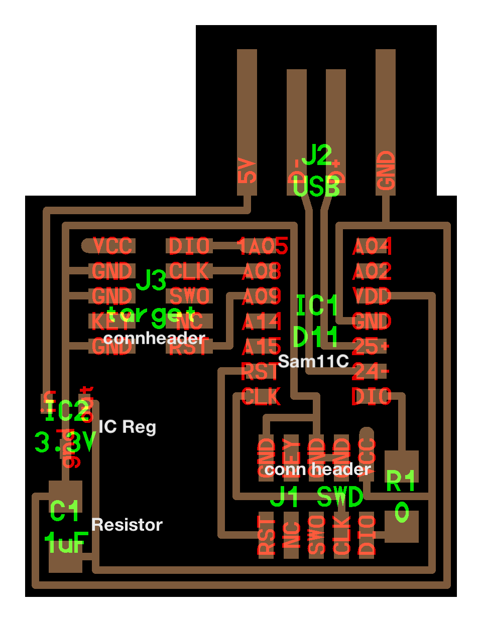
Still managed to make some mistakes, first took a SamD11D which has more pins so that was easy to find out, and the fact that the number in front of the name stand for the amount i could figure out since daniel wrote 2x
The soldering itself was not so difficult due to the fact that the component were all nice and big. Although soldering is always difficult and i did make the mistake to follow Daniel his video in which he actually started with the highest component which is not a good idea, but it worked and i did manage to put the Res0 in so no ugly wires going over my board.
But then the real challenge began.. programming the board.. which you need to do with another JTag something with a chicken and an egg.. After a few bugs with USB 3.1 going to USB 2.0, which were solved with patience, refresh and a bit of wiggling. Couldn’t find much in the Fab documentation about new MacPro combined with JTag programming so i had to turn to Henk for help.
We started with watching Neils video and after a lot of trial and errors we found out that my board is actually not working after a lot of resoldering and debugging it was still not showing up so back to the drawing board.

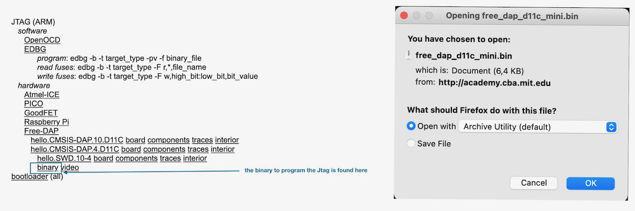
Here is where you can find the binary, which i have no clue yet on how to use it but who knows maybe i need it in 2 weeks.
Thankfully i was able to spend another couple of hours to make a UPDI and debug my JTag. The JTag is still not functioning as we speak, so far the REG and the SAM11C has been replaced just in case the REG was wrong (3.3V instead of 5V), visually hard to distinguish these two, but it seemed to have been the right one .. so far no success, i guess it becomes an ongoing project, or if i am lucky Henk can maybe help out to debug this.
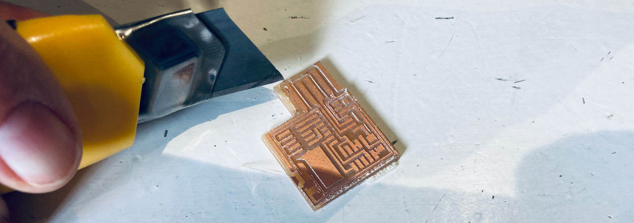
Soldering the UPDI was fun, although the FTDI (confused me a lot that there is a FPDI on the UPDI) in the middle is very hard to solder, since the legs are so tiny and close together. In my first try i started with heating the legs and putting lots of solder on it which i sucked with the sucker that is combined with a heater. This way of working frustrated me very much, the point of the heater is so blunt that you can’t really reach the right spot. By trying to do this i fucked up my board with all burning marks and ruined traces. I decided to mill a new board to start fresh and try another technical approach, this time i tried to solder all the legs separately and using a plier point heated up with the solderiron to remove the solder thats in between the pins.

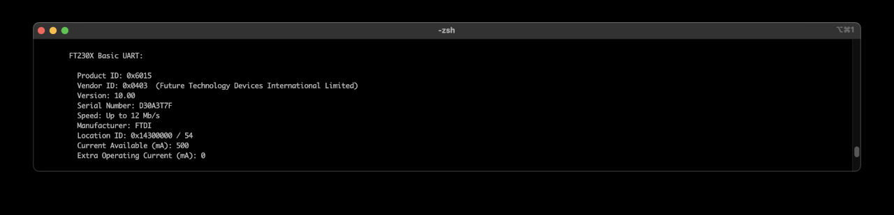
My computer read the UPDI :) this is accessible through: About this MAC/System report.
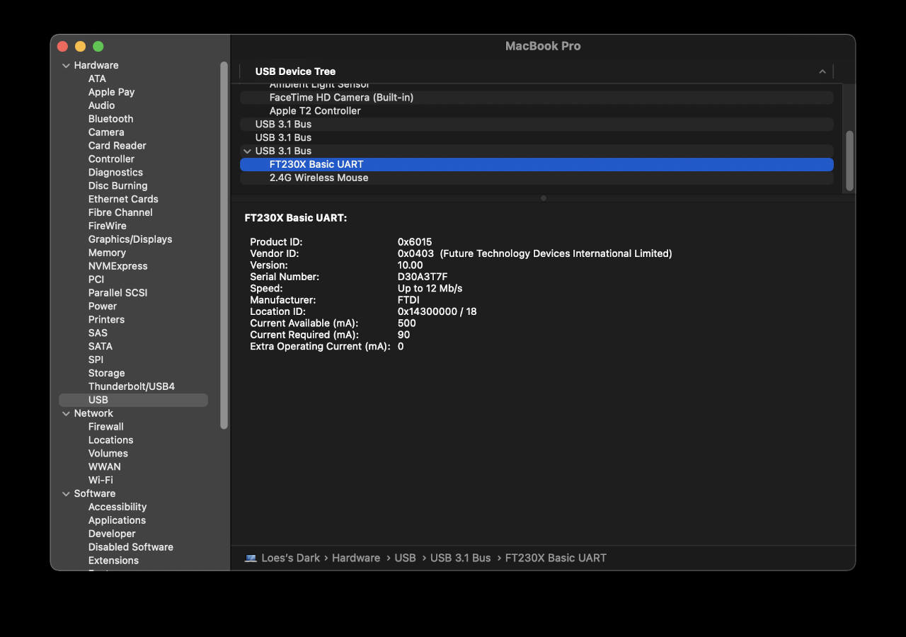 Or via terminal when you type:
~ % system_profiler SPUSBDataType
Git
when i tried to push my commit to Gitlab, it failed and gave me this message:
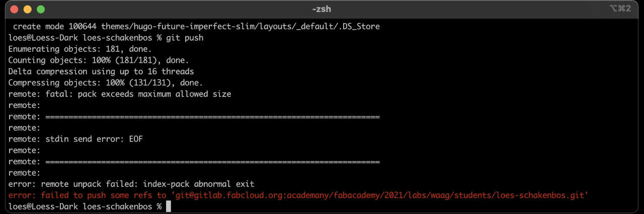
i first assumed that i did something wrong so i tried it again and again and again.. not smart in retrospective, now that i understand that the moment you enter the git commit - m 'whatever' it actually is already lined up to go and doesn’t leave. So i ended up putting commit onto commit etc.
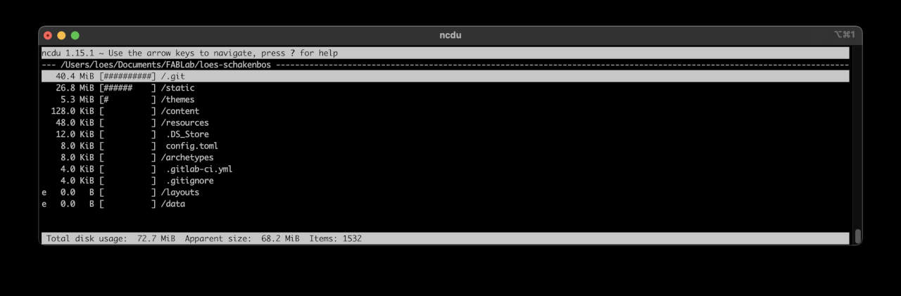
When i asked my group if they had experience with it, i got some great tips. So i started ready Paulas documentation on how she solved it which brought me to Hyejin Ahn her Fabsite and finally i was at the source on Gitlab. I installed NDCU which is a disk usage tool
brew install ncdu
then I went to my repository folder typed ncdu and you get something like this (this is after it was fixed)
Went through all the steps as described by Hyejin Ahn
- from 1 layer higher then you repository
cp -r loes-schakenbos loes-schakenbos.bak
check if it really exist - i use finder out of habit move one layer down to your repository
rm -rf .git
removes your Git repository
git init
To starts a new Git repository
cp ../loes-schakenbos.bak/.git/config ./.git/config
copies the original Git config from the backup directory to the current directory
already here i didn’t get a responds from Terminal which makes me wonder.
git add .
git commit -m "please work"
git push origin master -f # force push to the master
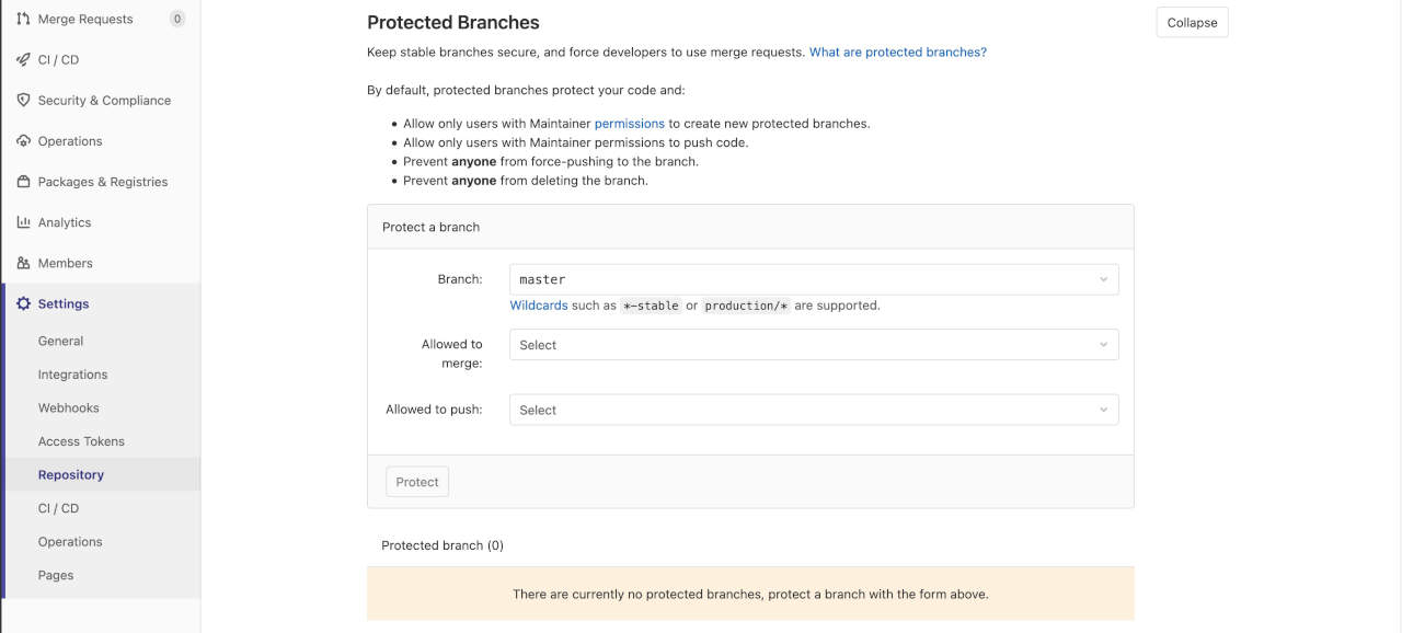
here i got the same error as before which i read in Hyejin Ahn that it could be a setting in the setting/repository/protected branches, which i did, press uprotect but unfortunately this did not fix the issue with me yet.. probably did something in between wrong, next time i should take it slower, saturday evening is not my favorite evening to be stuck behind a screen for a few hours even during corona times.
At one point i figured it would be smart to start all over again like in week 01 which shows i didn’t fully understood the issue otherwise i would have known it would be useless, the commits are still patiently waiting in line what ever you do.
So i decided after making another copy of my repository to go for the big steps and delete my commits. Some googling brought me to stackoverflow where it was clearly described on how to do it. By this time i figured that all is allowed in war and sleep deprivation so i gave it a try.
First typed im git log to see my commits, as you can see and if you can read dutch understand i was not so zen anymore.
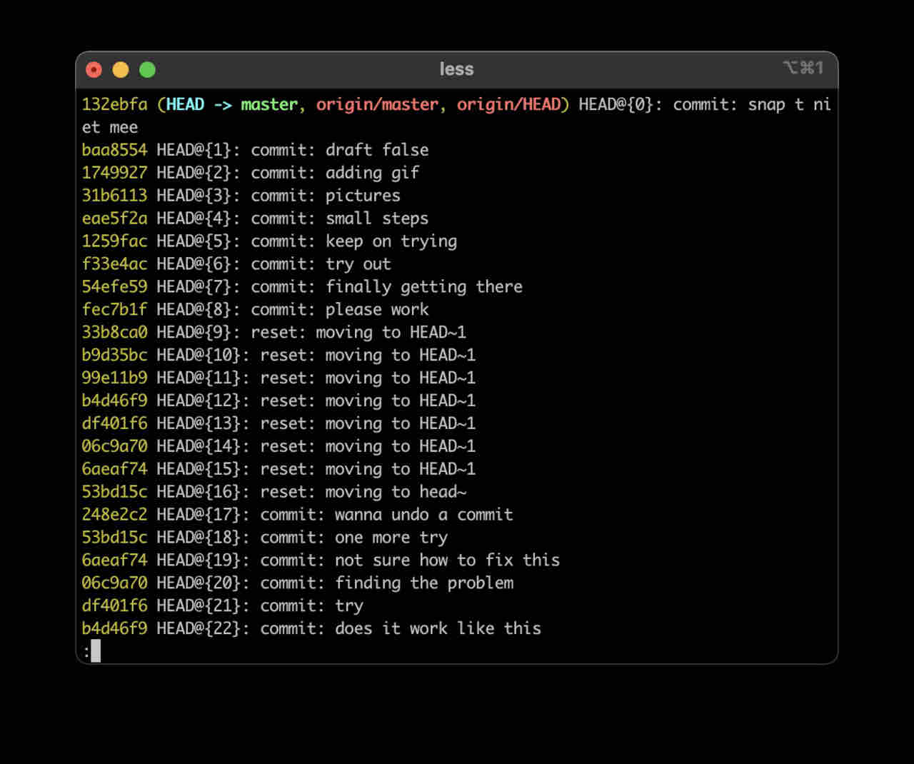
then i went for the brutal git reset --hard HEAD~1 and kept on doing this until i arrived at the safe spot before i wanted to commit my video which by the way was only 5Mb but combined with the pictures it was all to big.

Don’t think this is the legal way to go, but honestly i am just happy it worked.
For future reference repository cleanup
Basics
Some basics since i just came out of the egg when it comes to this subject:
-
ISP(AVR) 6- and 10-pin ISP header diagrams - The in-system programming (ISP) programming method
-
ATtiny hardware for ISP (also known as TinyAVR) are a subfamily of the popular 8-bit AVR microcontrollers, which typically has fewer features, fewer I/O pins, and less memory than other AVR series chips.
-
UPDI The Unified Program and Debug Interface (UPDI) is a one-wire interface for external programming and on-chip debugging of newer ATtiny and ATmega devices. (USB connection).
-
JTAG JTAG is a common hardware interface that provides your computer with a way to communicate directly with the chips on a board. It was originally developed by a consortium, the Joint (European) Test Access Group, in the mid-80s to address the increasing difficulty of testing printed circuit boards (PCBs). JTAG has been in widespread use ever since it was included in the Intel 80486 processor in 1990 and codified as IEEE 1491 that same year. Today JTAG is used for debugging, programming and testing on virtually ALL embedded devices.
-
ICE In-circuit emulation (ICE) is the use of a hardware device or in-circuit emulator used to debug the software of an embedded system.
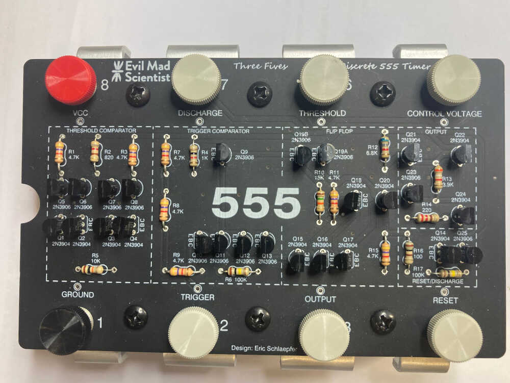
Below picture if of a 555, one of the first integrated circuits made. This model shows that inside an IC are actual electronic circuits and components extremely enlarged so thats its understandable for me :) Henk gave me a link to look into it a bit more. Appearently the 555 is a classic among the integrated chips.
| system | hardware |
|---|---|
| IS | ATtiny |
| UPDI | hello.serial-UPDI |
| JTAG | helloCMSIS |
- think i achieved my goal this week, have a clearer view of what i want but am not sure on how to do it yet.
 - more still to do this time, debug my Jtag further (or make a new one if all fails)
- now in Week09 we found out that edbg is now working on mac.
Files
No files to share this week
Links
link related to Jtag programming