
8 - ELECTRONICS DESIGN
Group assignment:Use the test equipment in your lab to observe the operation of a microcontroller circuit board send a PCB out to a board house Individual assignment:Use an EDA tool to design a development board to interact and communicate with an embedded microcontroller, produce it, and test it Extra credit: try another design workflow Extra credit: design a case for it Extra credit: simulate its operation
SDS7202 OSCILLOSCOPE
The SDS7202 oscilloscope is a key player in the world of electronics. I tell you, with its high resolution display, this oscilloscope allows us to see with an impressive level of detail the electrical signals we are analyzing. You know what's great? That thanks to its ability to capture complex signals with a very high sampling rate, we can understand how our circuits behave with great precision. From circuit design to troubleshooting electronic systems, the SDS7202 is like a window that allows us to look directly into our circuits. And best of all, its interface is very easy to use, with plenty of functions that help us measure and analyze our signals quickly and accurately.
Note: A signal generator is an electronic device that produces electrical signals of different shapes, frequencies and amplitudes in a controlled and precise manner.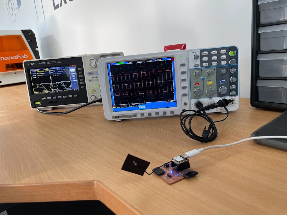
- On/Off button: Turns the oscilloscope on or off.
- Vertical adjustment control knobs: Adjust the vertical scale of the signal being measured on the screen.
- Horizontal adjustment control knobs: Adjust the horizontal scale of the signal being measured on the screen.
- Signal coupling knobs: Allow to select the type of input coupling for the signal (AC, DC, GND).
- Trigger adjustment buttons (Trigger): Allows you to set the level, slope and other trigger characteristics to stabilize the waveform on the display.
- Calibration button: Allows to perform a calibration of the oscilloscope to ensure accurate measurements.
- Navigation and menu buttons: Allow scrolling through the menus and options of the oscilloscope.
- Channel selection buttons: Select the input channel to be displayed and configured
- Acquisition stop button (Stop): Stops the acquisition of signals to analyze a specific capture.
- Display control buttons: Allow you to adjust the display on the screen, such as brightness intensity, contrast, etc.
Group assignment
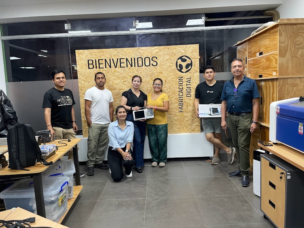
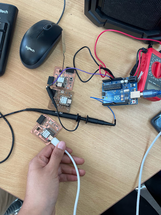
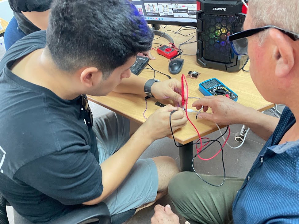
On March 15, 2024, we visited IEST Simon Bolivar in Callao for our group assignment. During the visit, we had the opportunity to use oscilloscopes to test the functionality of our circuit boards. We performed several tests on different boards and discovered that some of them were not working properly, the leads were very thin and some were very worn, which we were able to identify thanks to the signals shown on the oscilloscope. Through this exhaustive process, we confirmed that the errors were not due to problems with the oscilloscope itself. This experience allowed us not only to detect problems on our boards, but also to become more familiar with the use of the oscilloscope in the context of our project.
TESTING
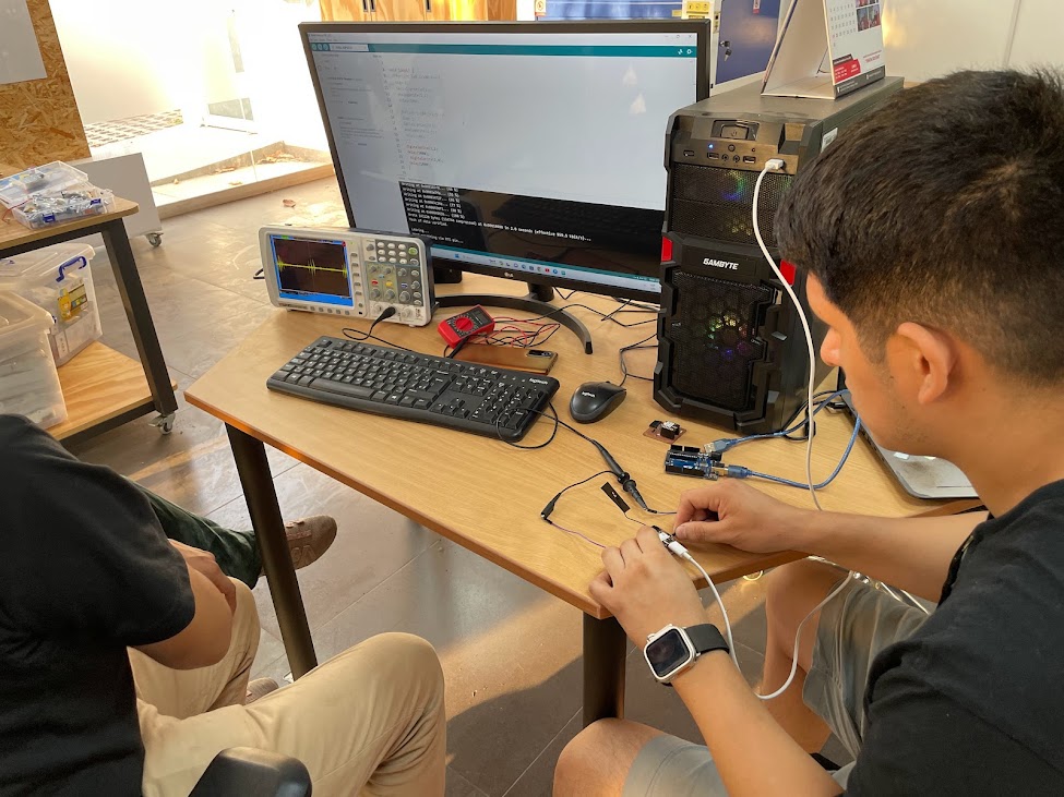
When we look at the oscilloscope image, we notice that we are receiving the signal from the program we have placed on our Quentorres board. And the best thing is that everything seems to be in order according to what the oscilloscope shows! This is really encouraging and tells us that our design is working as we expected. However, even though everything seems to be fine so far, it is important to continue to perform additional tests to ensure the consistency and reliability of our system. In addition, we must carefully document our results and conduct further tests to confirm that our board is performing stably under various conditions
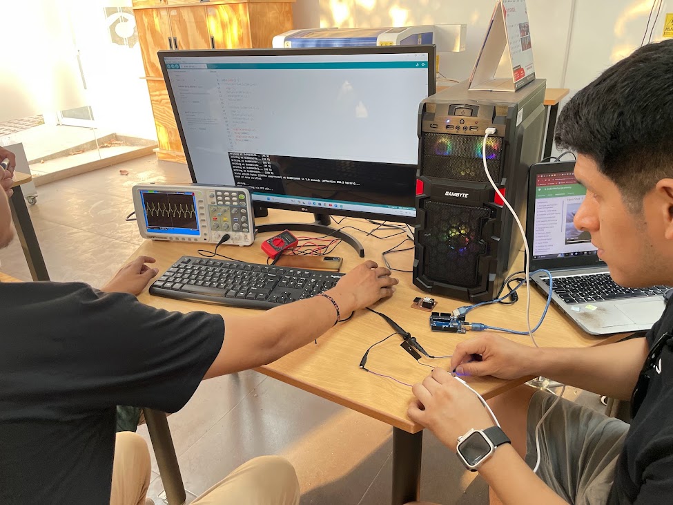
In the picture, we can see the various plates belonging to my friends and me. We were running tests to make sure everything was working properly. It's great to see how each of us is progressing on our projects and how we are working together to make sure everything is in order. We are committed to the success of each of our designs and are willing to work together to make it happen. I'm excited to see how each board develops and hope we all reach our goals successfully.
-
With the multimeter, I can measure several important things on our boards. For example, I can measure the voltage at different points in the circuit to make
sure the components are getting adequate power. I can also measure the current to verify that there are no overload problems. In addition, I can measure the
resistance of the components to make sure they are within the expected limits. I can even check the continuity of the electrical connections! is an excellent tool for our practices.
-
The oscilloscope allows us to see how the electrical signal behaves over time.
I can observe the waveform of the signal and measure its amplitude, frequency and period.
This is useful for understanding how our circuits are performing and for detecting problems such as ripple in the power supply. I can also measure the pulse width of digital signals, which is useful for verifying the accuracy of the pulses in our control circuits.
Conclusions
Individual assignment
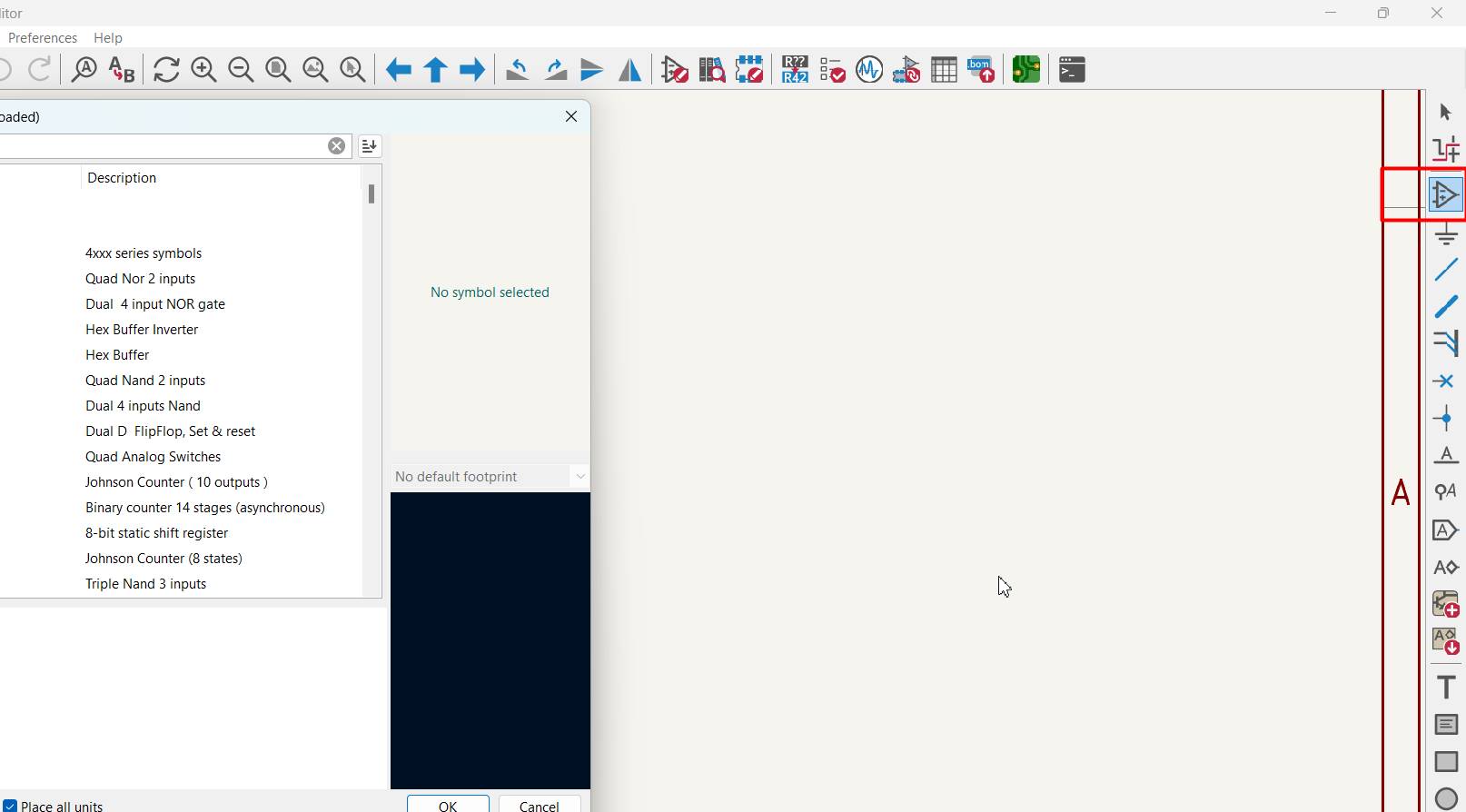
To import a footprint library into KiCad:
- Download the Library: First, ensure that you have downloaded the footprint library (usually in a .pretty format) that you want to import into KiCad.
- Launch KiCad: Open the KiCad software on your computer.
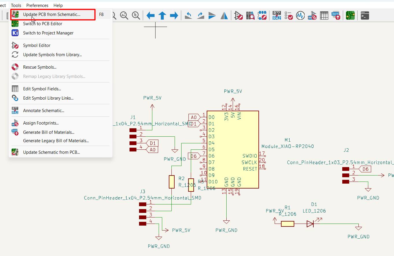
- Footprint Editor: In KiCad, navigate to the Footprint Editor. You can find this under the "Tools" menu in KiCad8, "Edit" menu.
- Footprint Libraries Manager: Once you are in the Footprint Editor, go to the "Preferences" menu and select "Footprint Libraries Manager."
- Add Library: In the Footprint Libraries Manager, click on "Append Library" or "Add" (depending on the version of KiCad you are using).
- Locate Library: Navigate to the location where you downloaded the footprint library, select the library file (.pretty format), and click "Open."
- Locate Library: Navigate to the location where you downloaded the footprint library, select the library file (.pretty format), and click "Open."
- Close Manager: Once you have added the library, close the Footprint Libraries Manager.
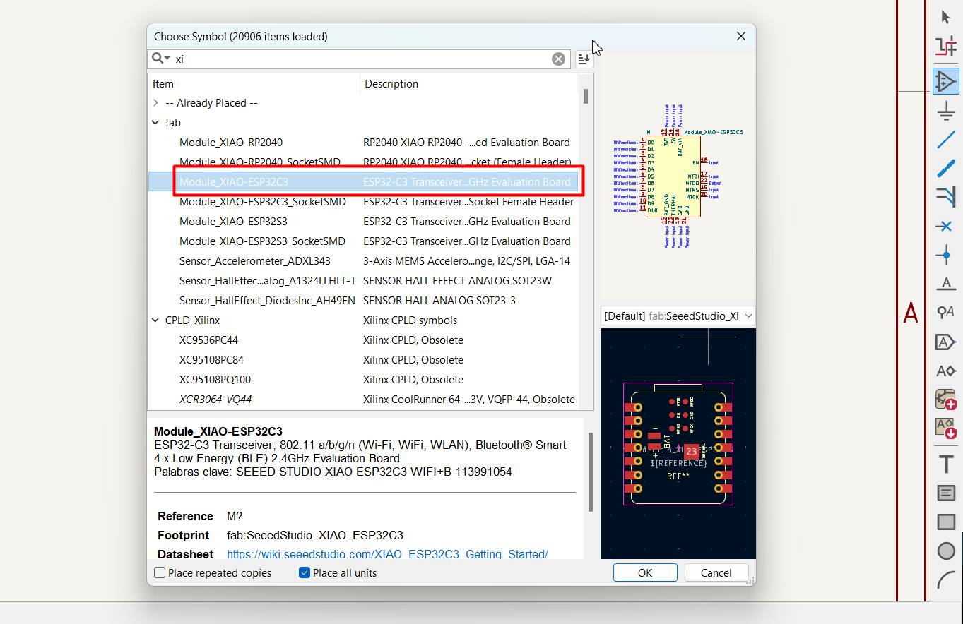
- Use Footprints: You can now use the footprints from the imported library in your KiCad project. When selecting footprints for components, you'll be able to see the footprints from the imported library in the Footprint Browser. LIBRARY LINK
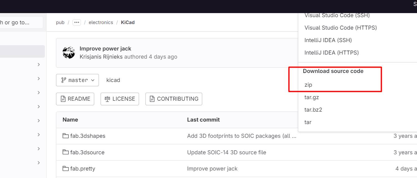
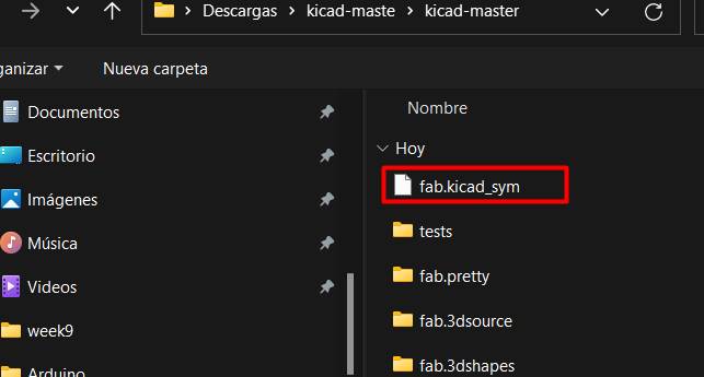
Download it in ZIP format to obtain the liberia files as shown in the photo.
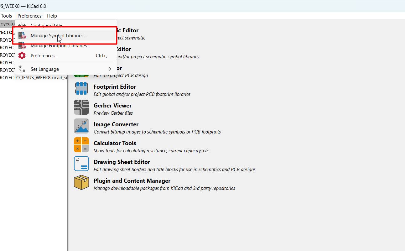
 It seems like you're providing a step-by-step guide for importing symbol libraries specifically in KiCad. Here's a refined version of your instructions:
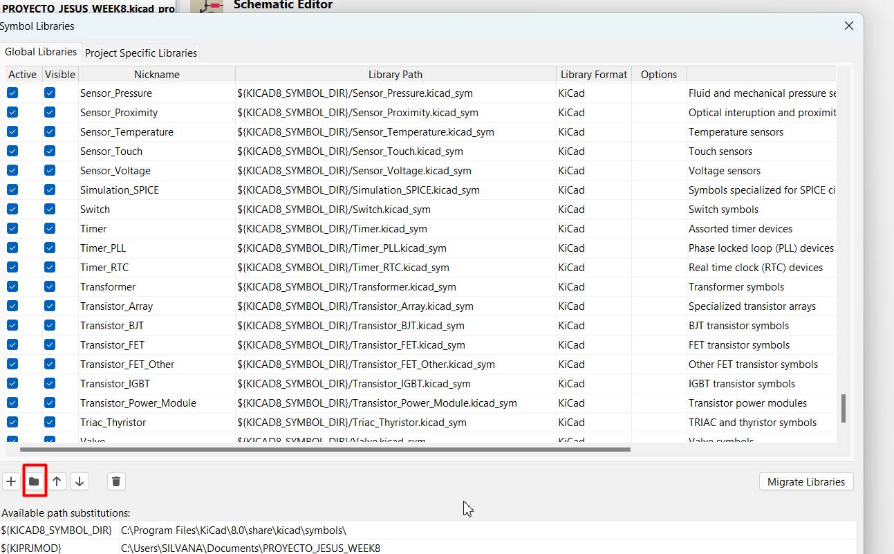
- Open KiCad and navigate to the "Preferences" tab.
- Choose "Manage Symbol Libraries" from the options.
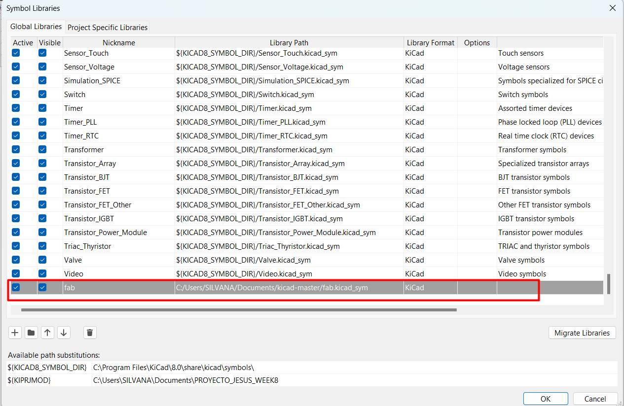
- lick on the folder icon to browse for the file
- Once you've located the file, click "Open".
- You'll notice that it has been added to the list of libraries.
- Finally, click "OK" to confirm and save the changes.
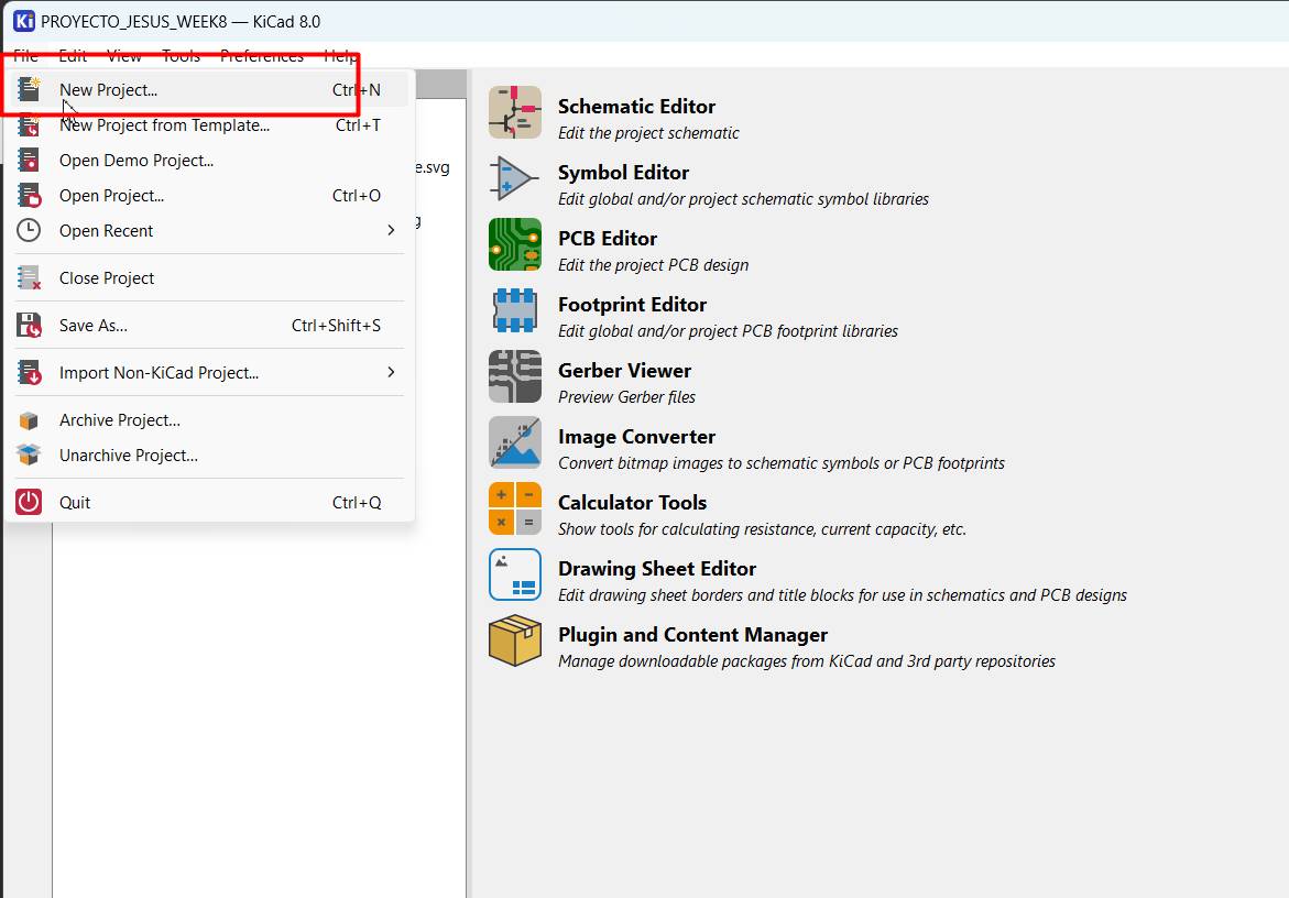
New proyect
Files > new project .
- A dialog box will open. Here, choose a name for your project and select the location where you want to save the project on your computer. Click "Save" or "Save."
- KiCad will automatically create a folder for your project in the location you select. This folder will contain all the files related to your project.
- Once you have created the project, KiCad will open the Project Manager. Here you can see a list of the files associated with your project and access different tools and options to work on your design.
- Now you are ready to start designing your board. You can open the Schematic Editor to draw your circuit schematic, and then move to the PCB Editor to design the printed circuit board.
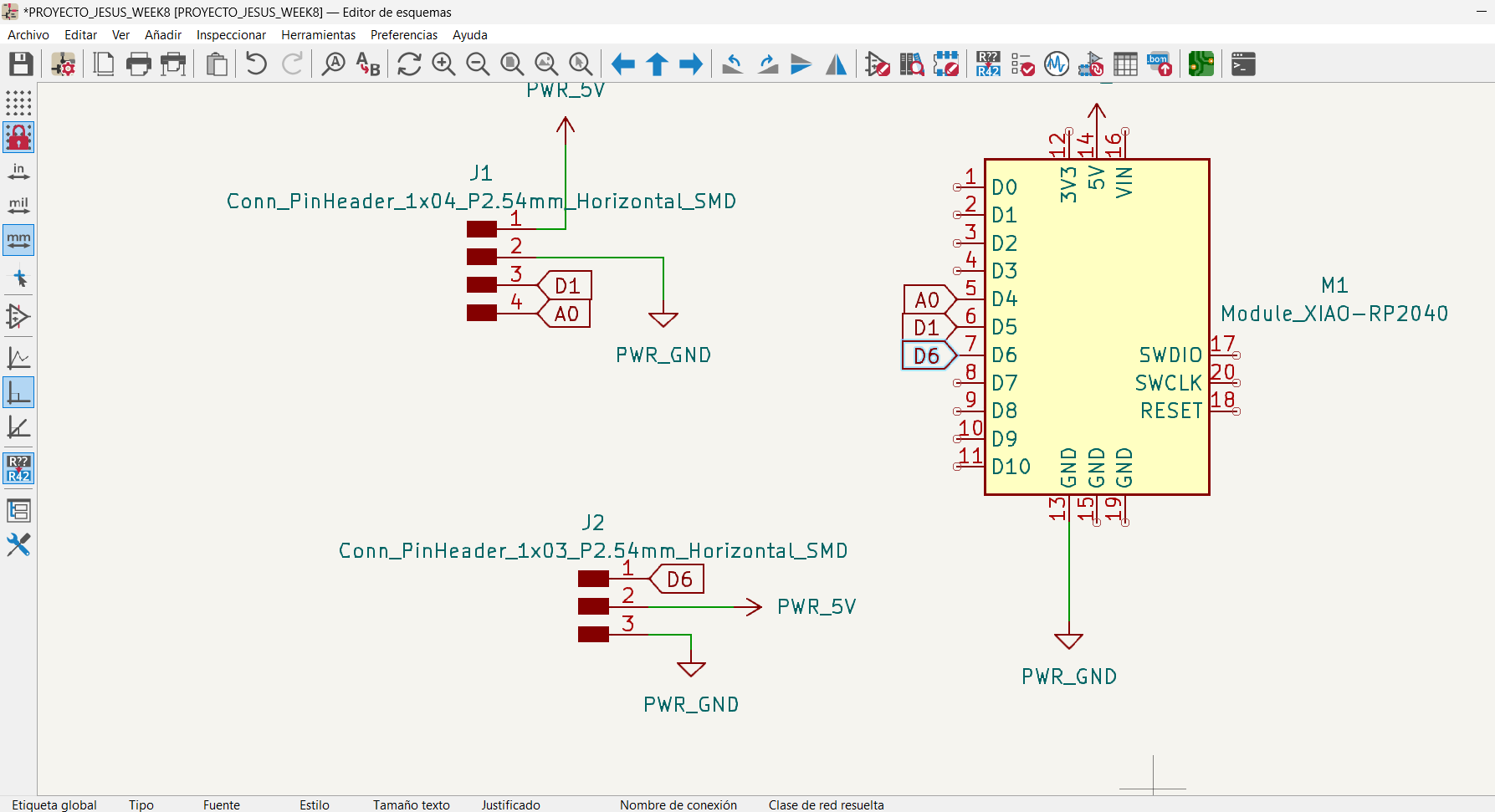
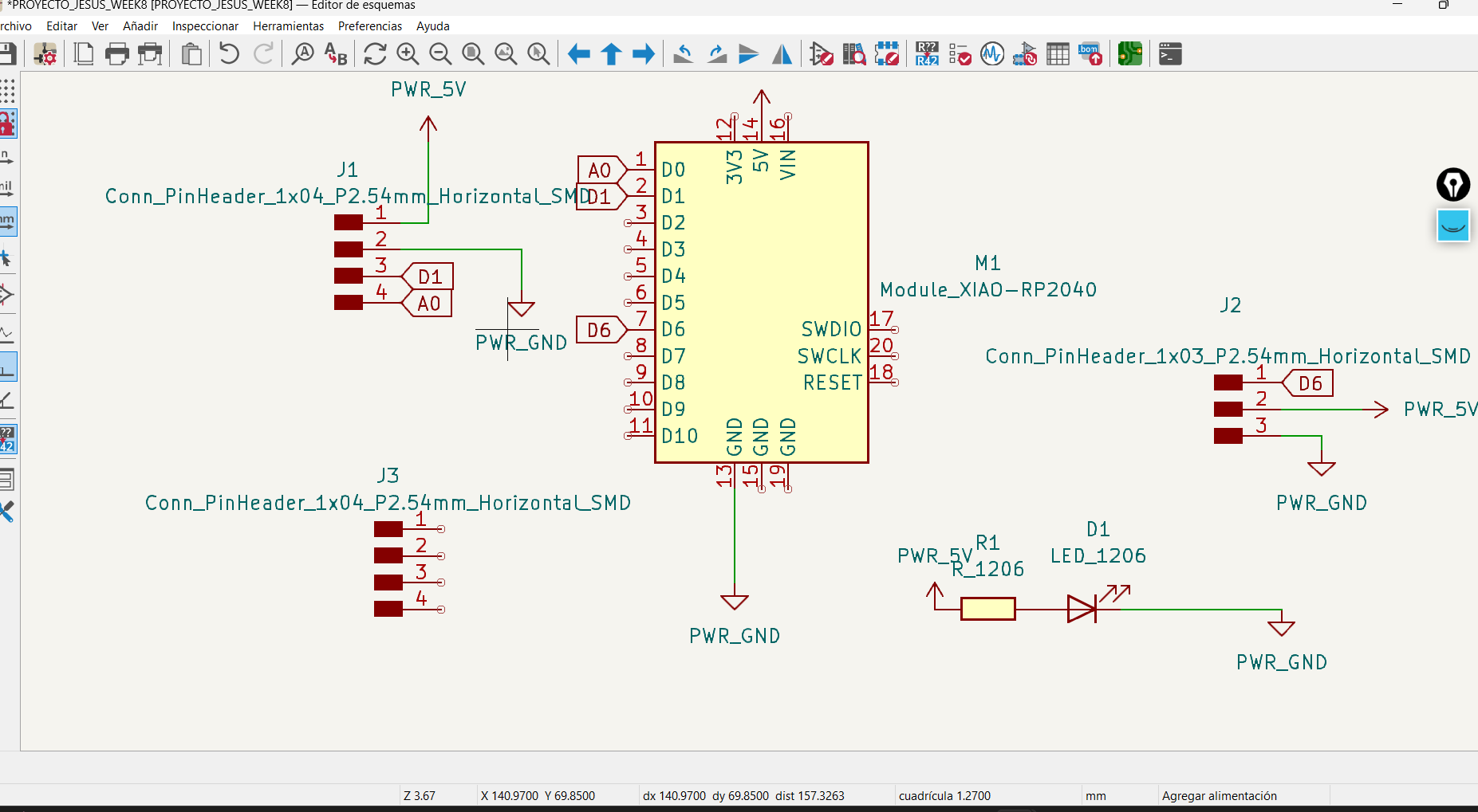
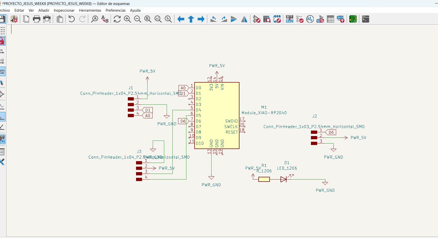
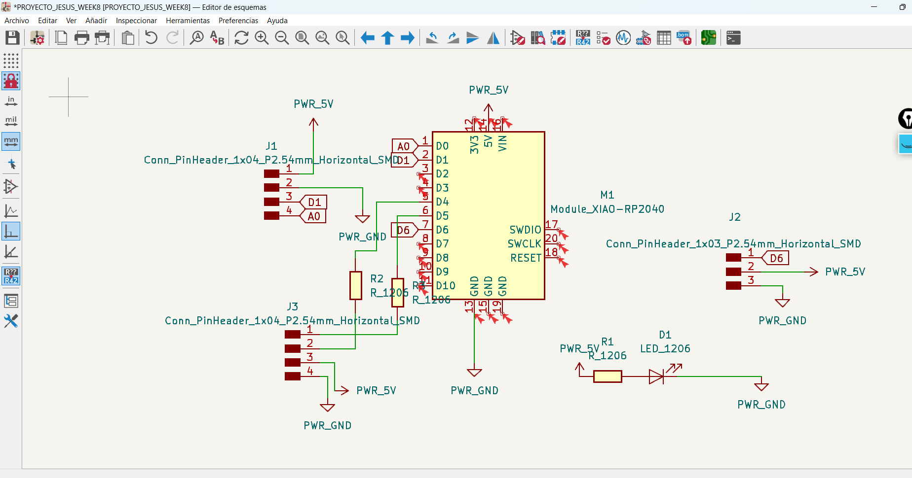
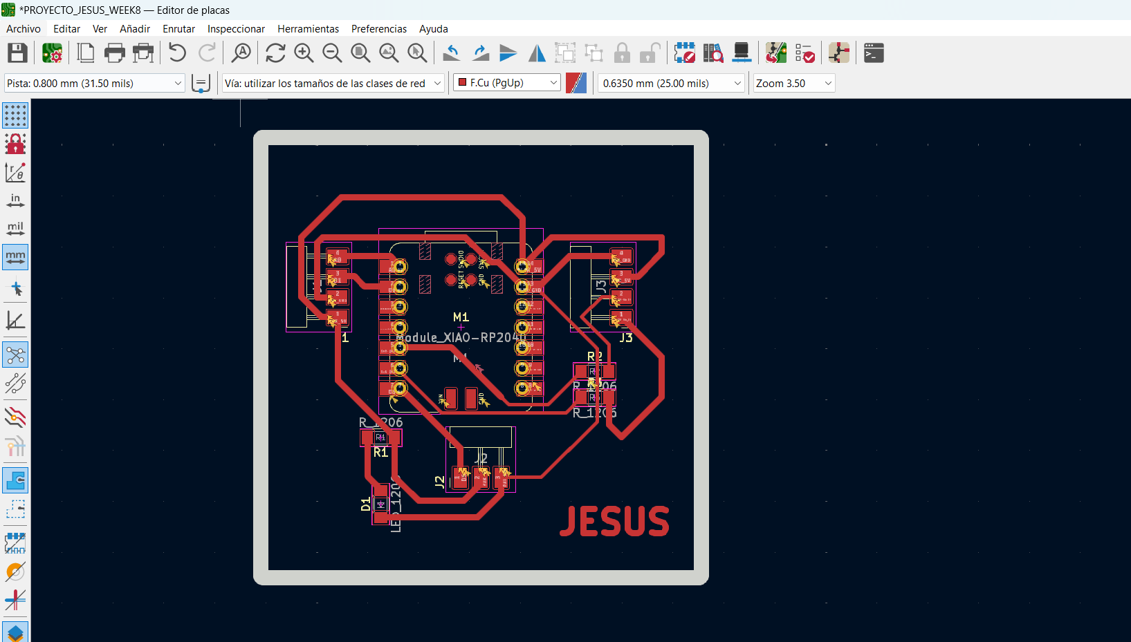
I must first connect the components of my circuit. To do this, I selected the track tracing tool on the toolbar and began connecting the pins of my components following the schematic layout. One of the first considerations I made was to follow the PCB layout rules. I remembered to avoid unnecessary crossovers, maintain proper distances between leads, and avoid sharp angles whenever possible. This would ensure that my design would be easy to fabricate and function properly once completed. I prioritized the connection of the power and ground leads, as they are crucial to the proper functioning of the circuit. I used wider leads for these connections to minimize resistance and interference. Next, I made sure to route the signal tracks efficiently, keeping them as short as possible to reduce interference and ensure reliable circuit performance.
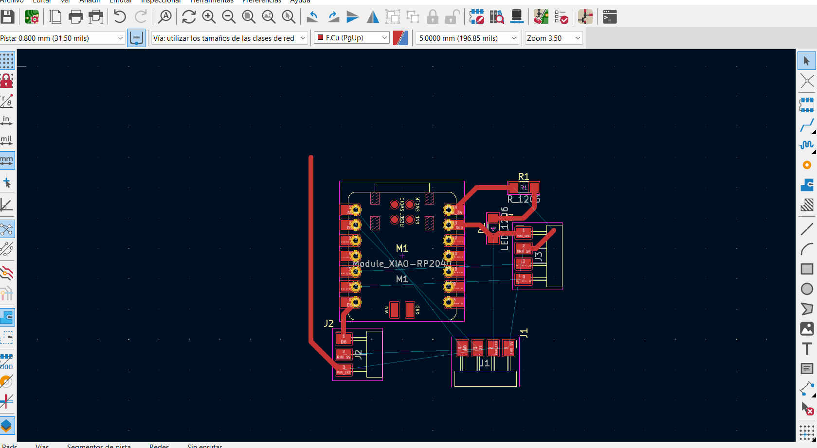
As I went through the process, I reviewed my design several times to optimize the tracks and make adjustments as needed. I made sure that all connections were complete and that there were no redundant or unnecessary tracks that could complicate the design. I used KiCad's review tools to verify the design rules and troubleshoot any problems I found.
EXPORT TO MODS
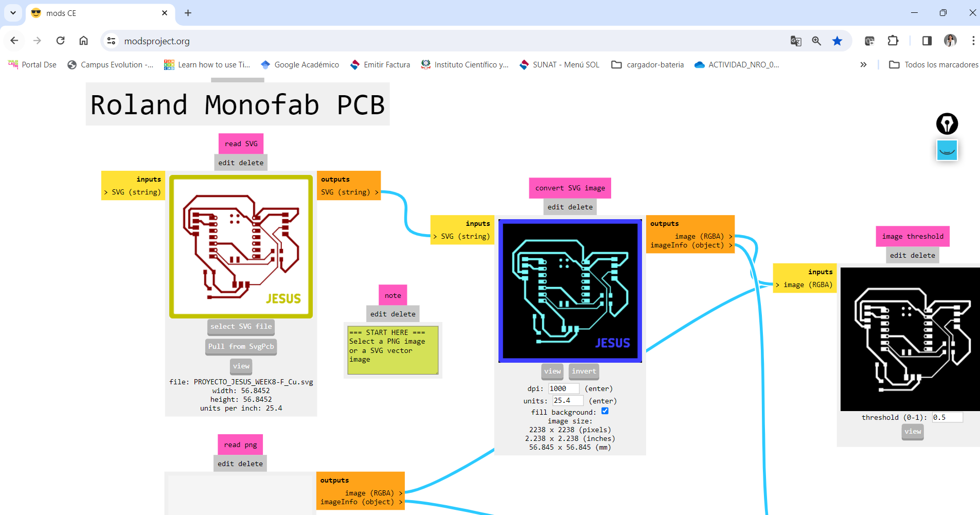
Export your design from KiCad: Open your PCB design in KiCad and export the design in SVG format. Verify that the export is successful and that the SVG file contains all the layers and details needed for your project.
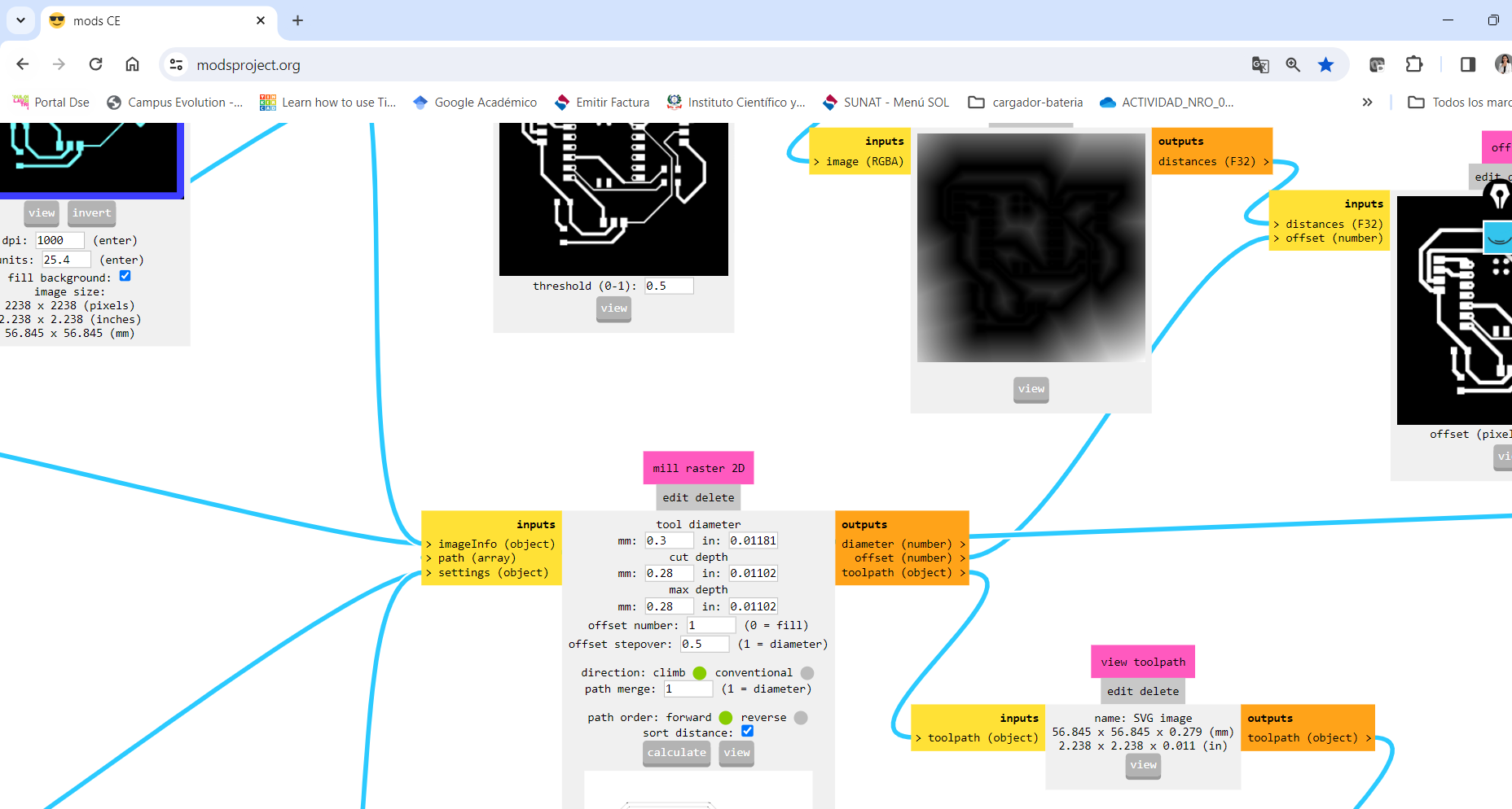
Edit "Tool Diameter" to 0.3: In the MODs interface, look for the option to edit the tool diameter or "Tool Diameter". Enter the value 0.3 in the corresponding field to set the tool diameter to 0.3 units.
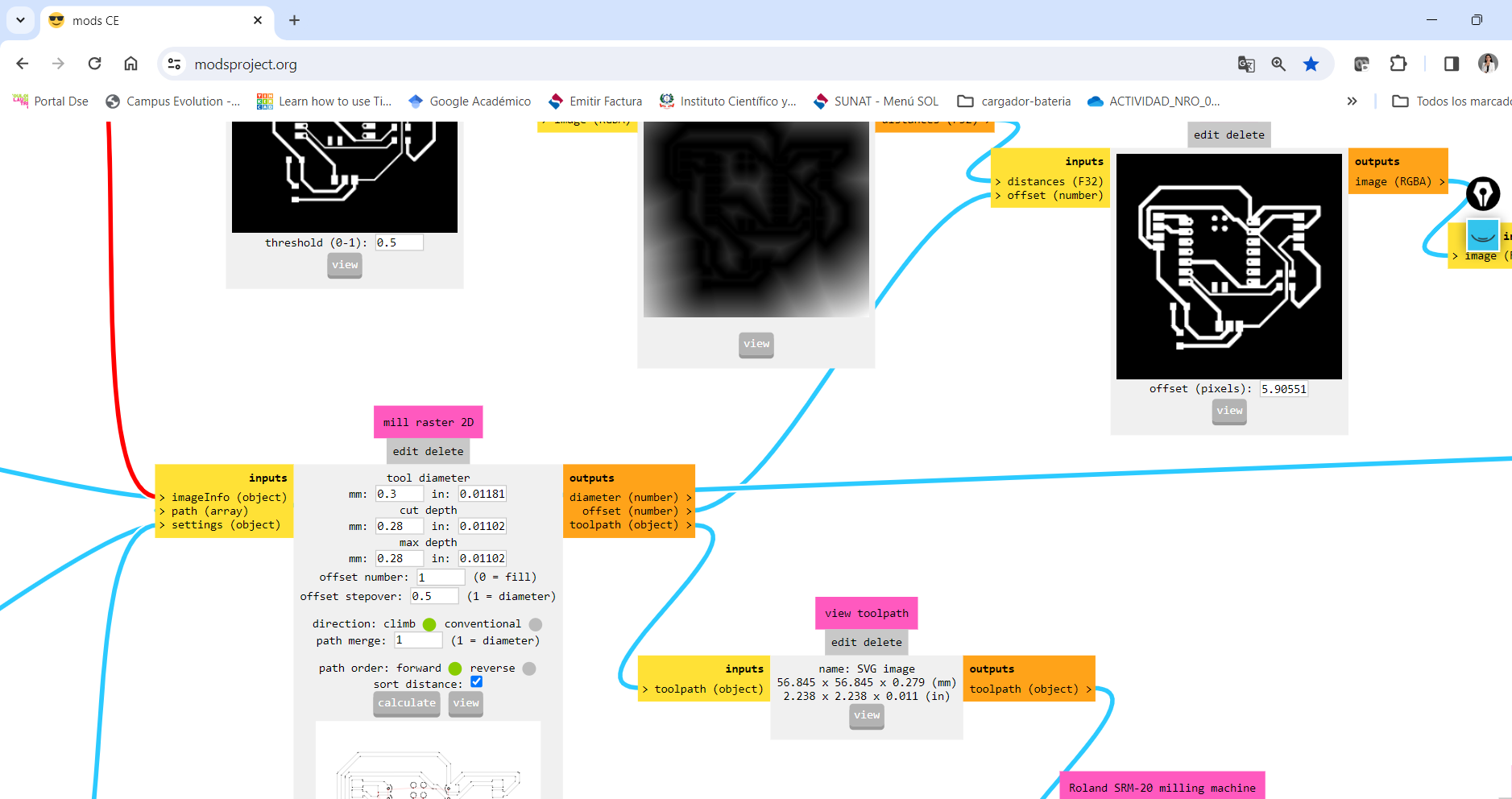
Set "Max Depth" to 0.28: Find the setting to set the "Max Depth" or maximum depth of cut. Enter the value 0.28 in the corresponding field to set the maximum depth of cut to 0.28 units.
Set Cup Depth to 0.28: Find the setting to set the Cup Depth. Enter the value 0.28 in the corresponding field to set the depth of cut to 0.28 units.
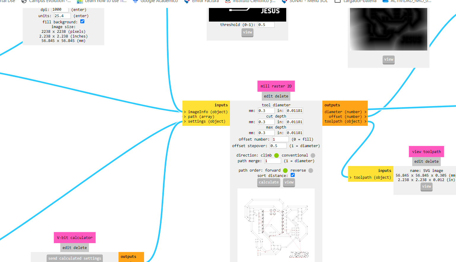
Select "Offset Number 1": If you have the option to select the "Offset Number", choose the number 1 to indicate that you want to use the first offset.
Calculate: Once you have made all the necessary settings, look for the option to calculate or generate the cut file.
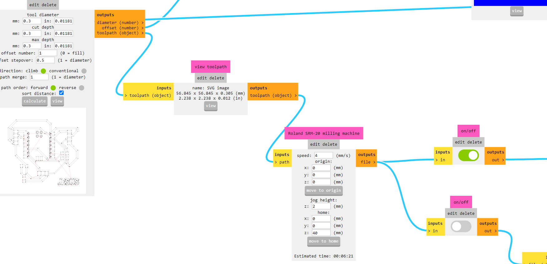
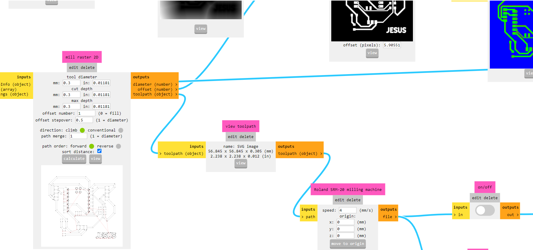
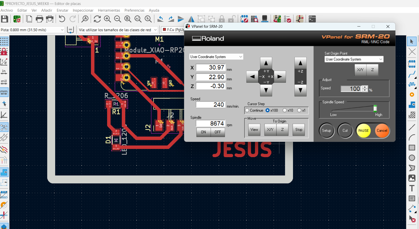
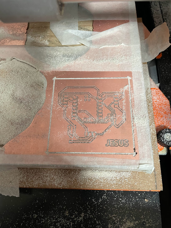
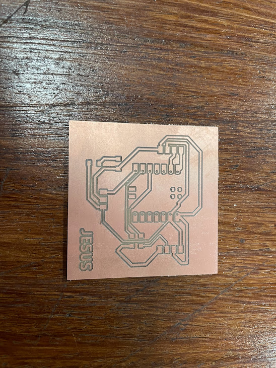
MANUFACTURING THE PIECE IN THE ROLAND
Conclusion
Link
- Mods
- Introduction to KiCad
- KiCad
- User Manual Owon SDS7202V oscilloscope
- Adrian Torres
- Short and sweet: pull up/pull down resistors explained
- Arduino IDE.
- Fab Electronics Library for KiCad
- Seeed Studio XIAO ESP32C3 proyect