BACK TO HOME PAGE
WEEK 6
ELECTRONIC DESIGN
WEEK ASSIGNMENTS:
Tasks for a week
Task:01 To make PCB board:
What is electronic design?
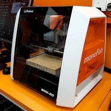
Machine used:
Software used:
This week assignment content:
INDIVIDUAL ASSIGNMENTS:
PROBLEMS:
Individual Assignments:
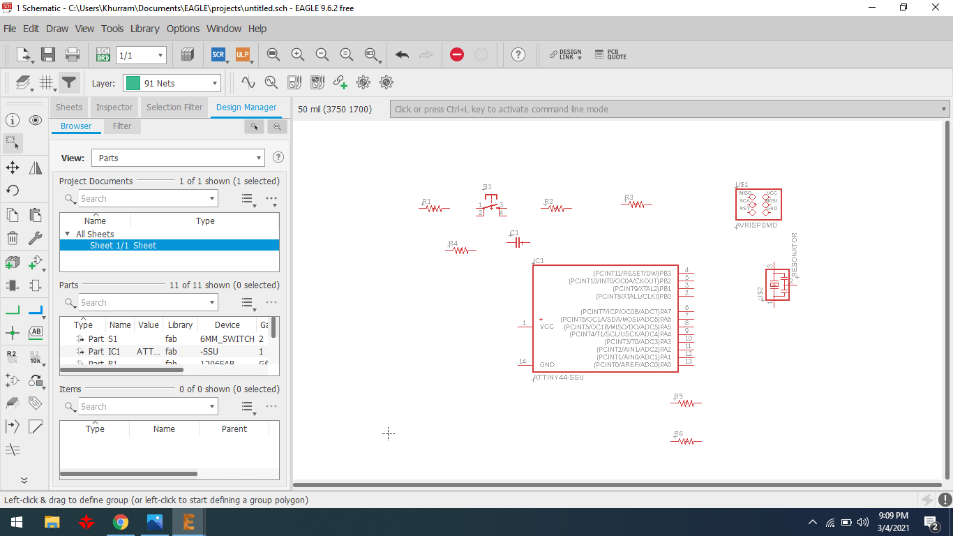
Schematic Design:
Create a new schematic diagram.
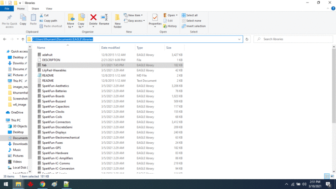
Downloading Library from previous student's archive.
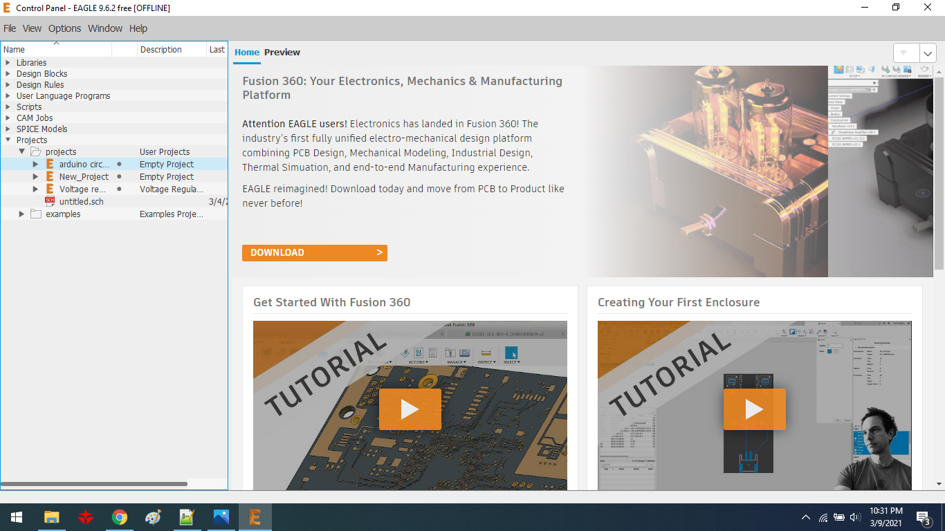
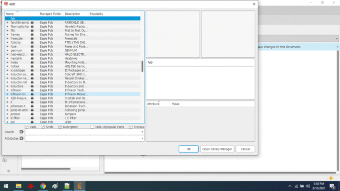
How to add library in eagle software?
Steps:
To make a Schematic diagram:
Steps:
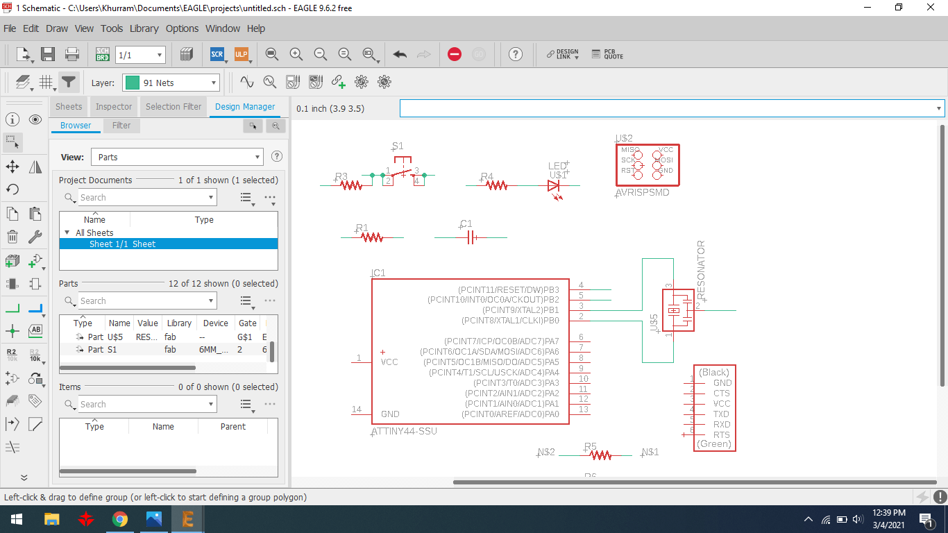
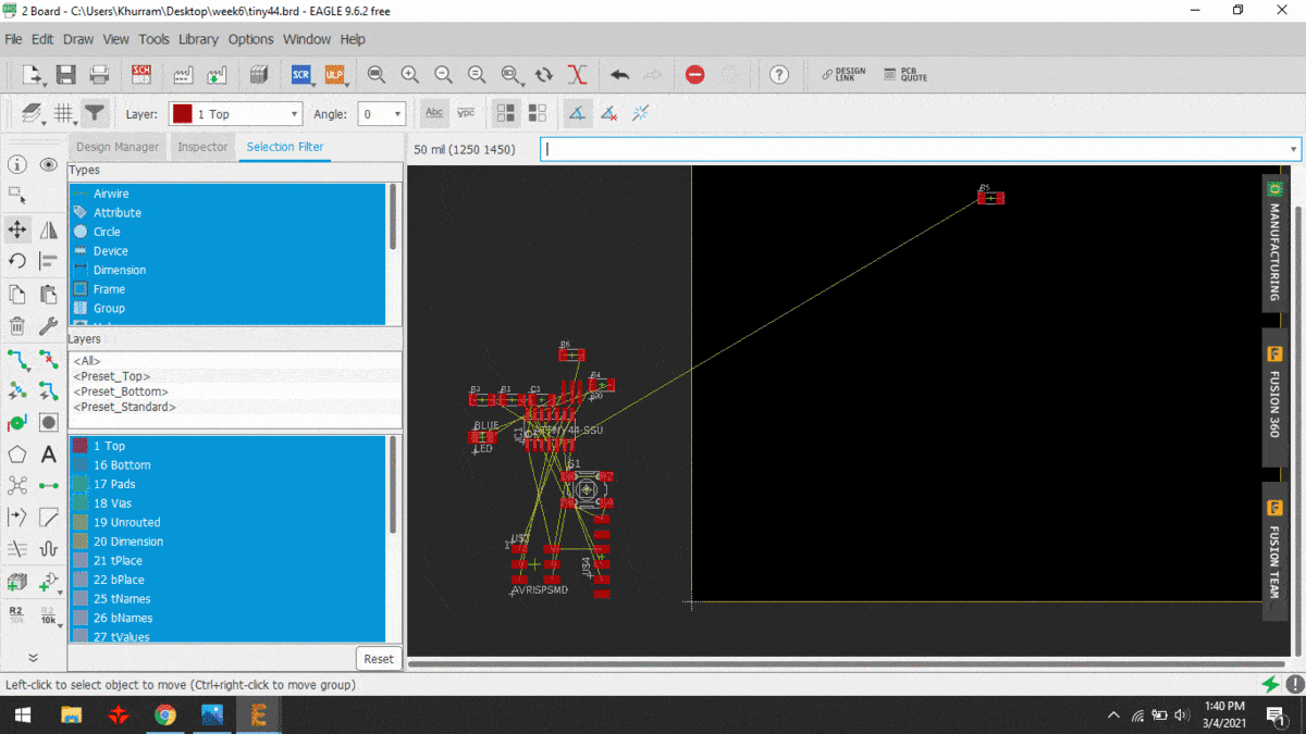
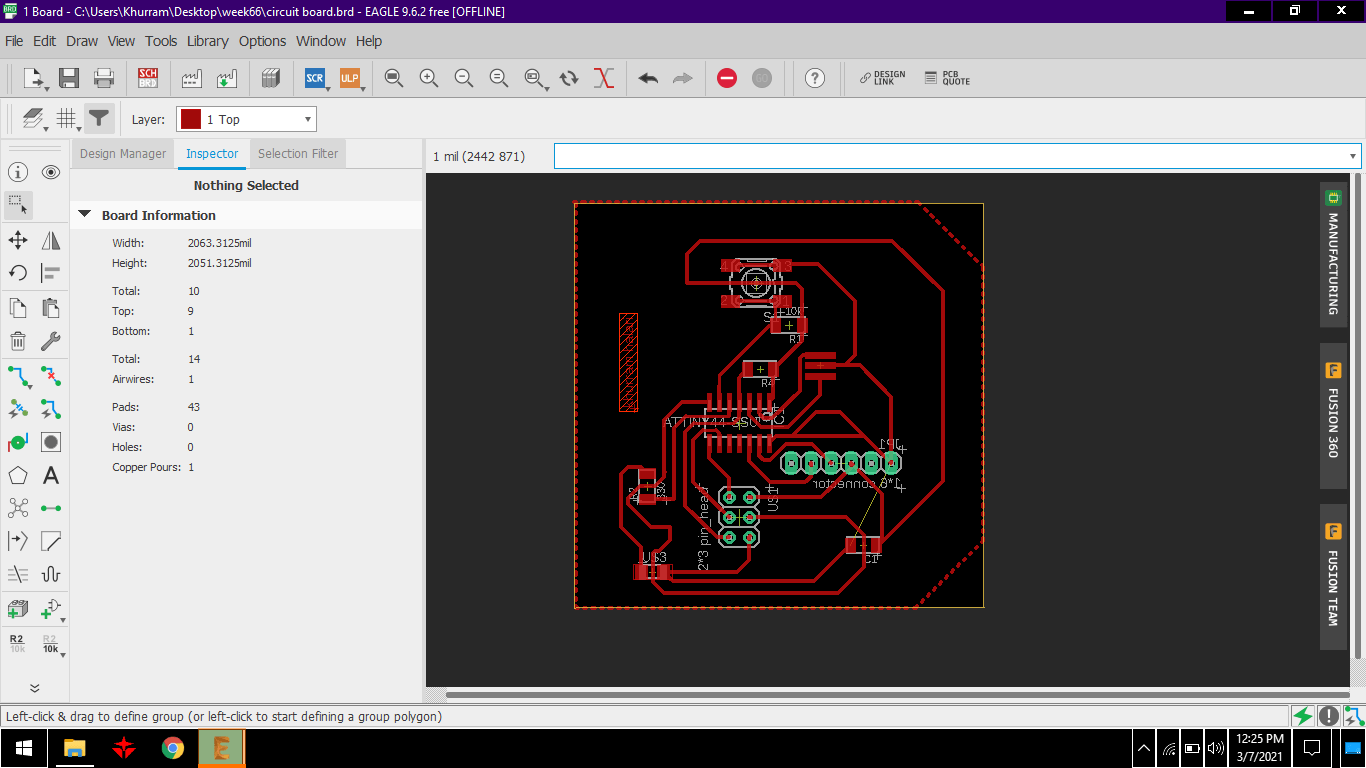
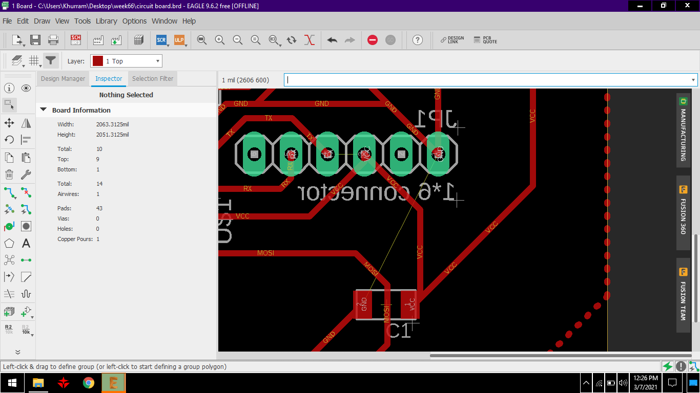
I have completed the schematic diagram of the hello echo board and then I have designed the actual board by shifting from the schematic to PCB and making a route of components.
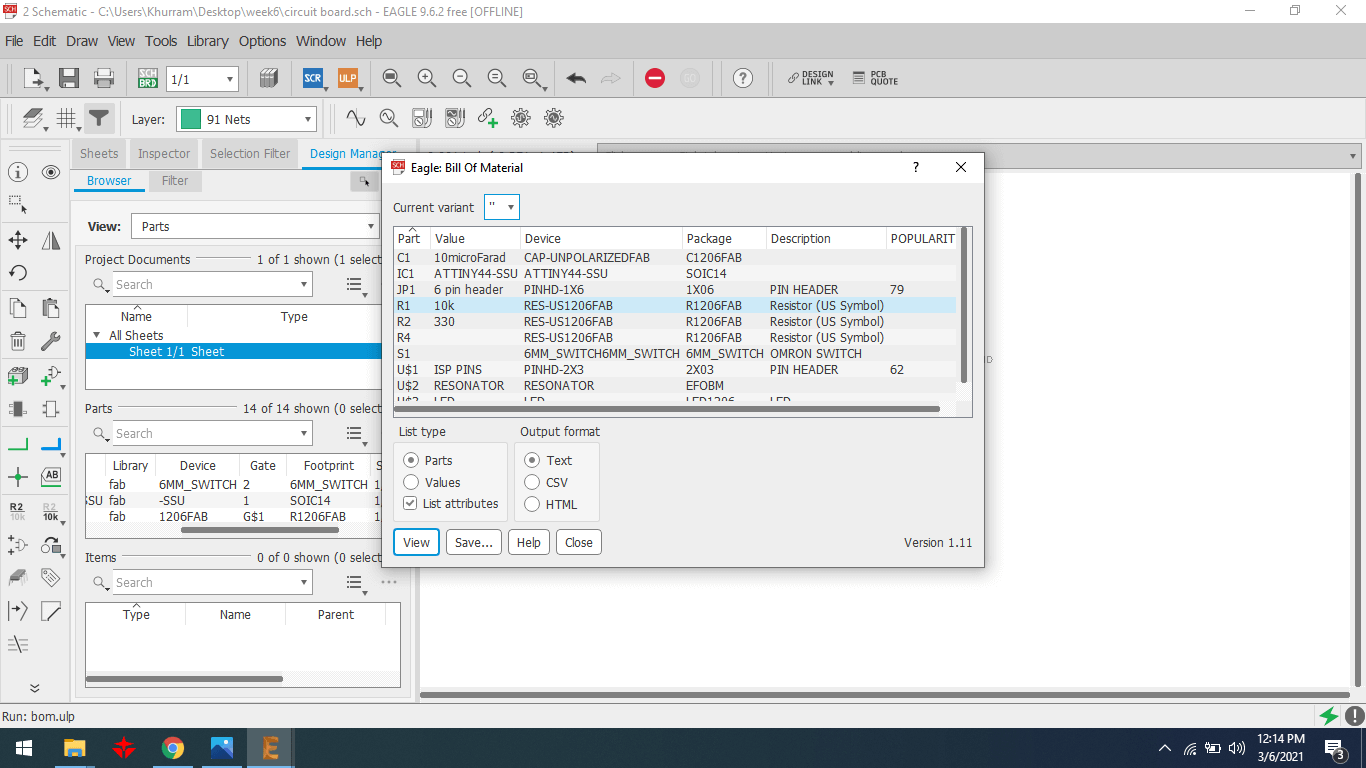
Bill of material.
Incompelete Design:
First Attempt:
This is my first PCB design in which the width of the Layer is 10 mil it is a very small size because I did not have an idea then my local instructor is telling me about the layer size.
Second Attempt:
This is the second PCB design I can not found routing of the last components because the layer of the last components are intersected with each other.
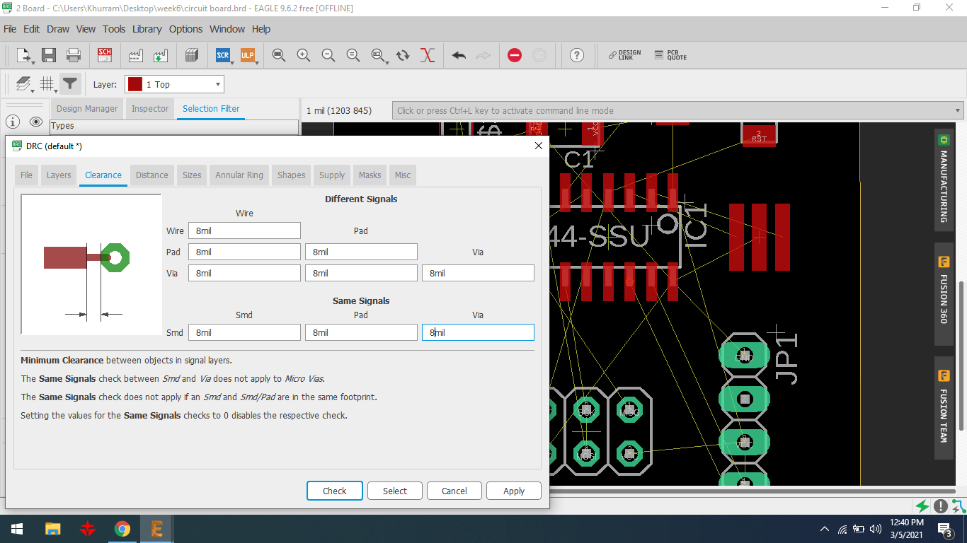
Change width size of PCB layer before making rout of PCB components I never forget to change the width of PCB layer.
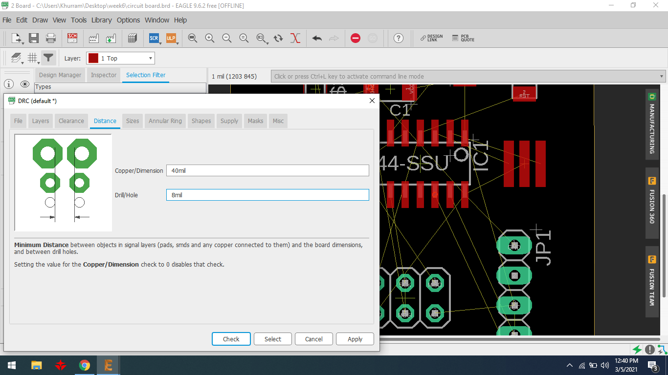
Go to the DRC option from the left tool bar and then go to the distance option and change the width size and drill hole size.

Change the width of some layers because these layers intersect with each other because of not much space between the IC pads.
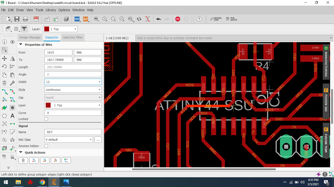

When I have completed routing and generate rml file into fab modules then I have known about the layer intersection before I did not die of layer intersection.
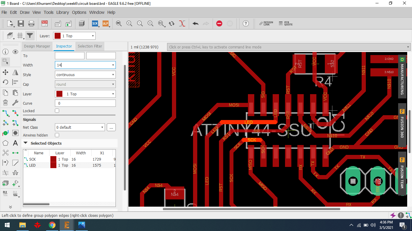

Creating space between layers.
I can not be connecting the last trace of components.
I was trying and found another way to connect the last layer.
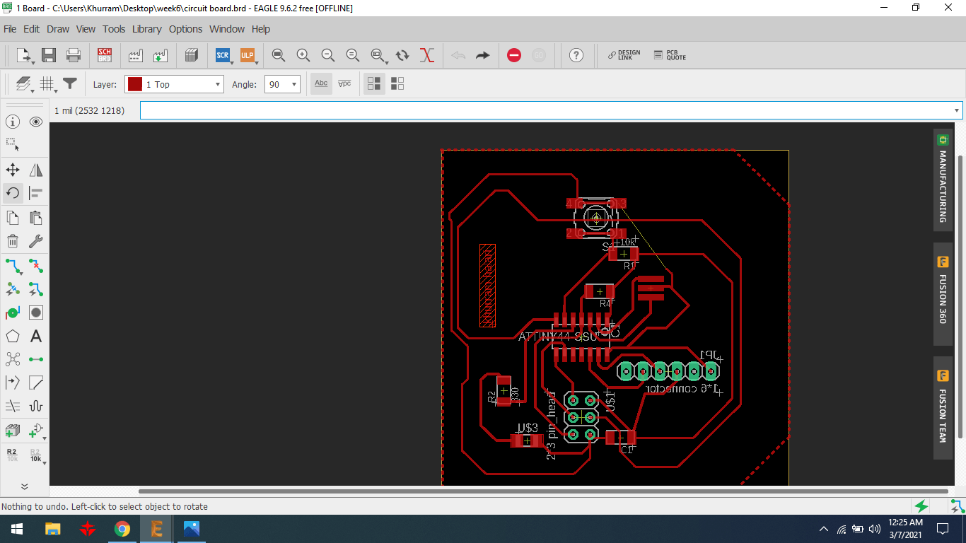
I did not want to connect a zero-ohm resistor to my circuit. But in the last, I have an idea in my mind to change the pin name of 2*3 pin header so this is the better way to avoid the zero-ohm resistor.
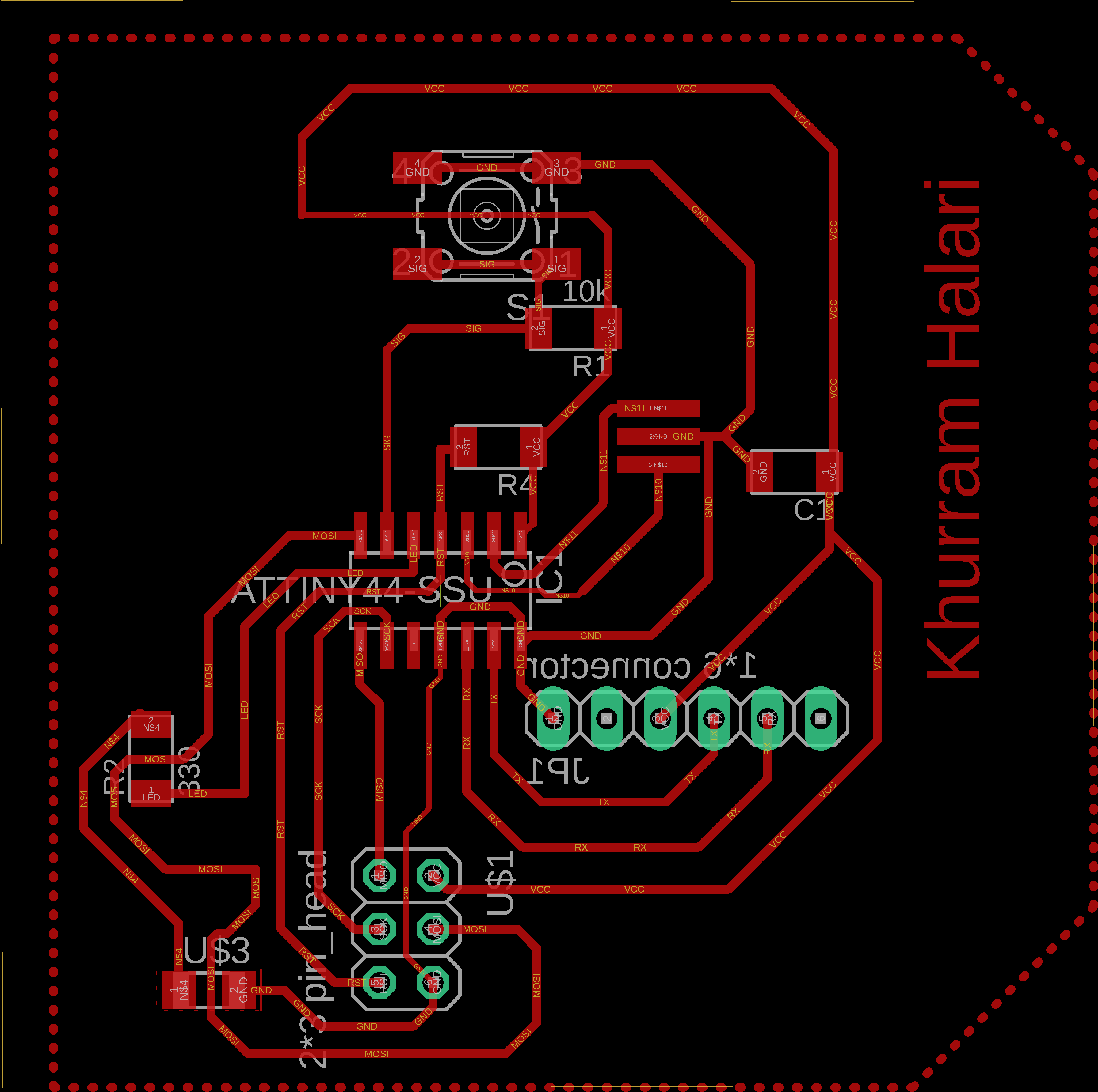
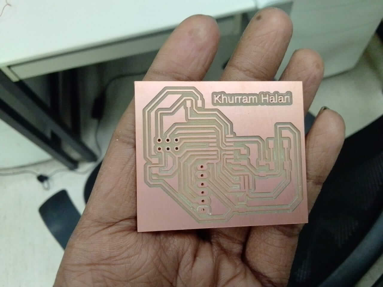
This is my final PCB diagram. After face some problems I am able to do this task.
To make png file steps:
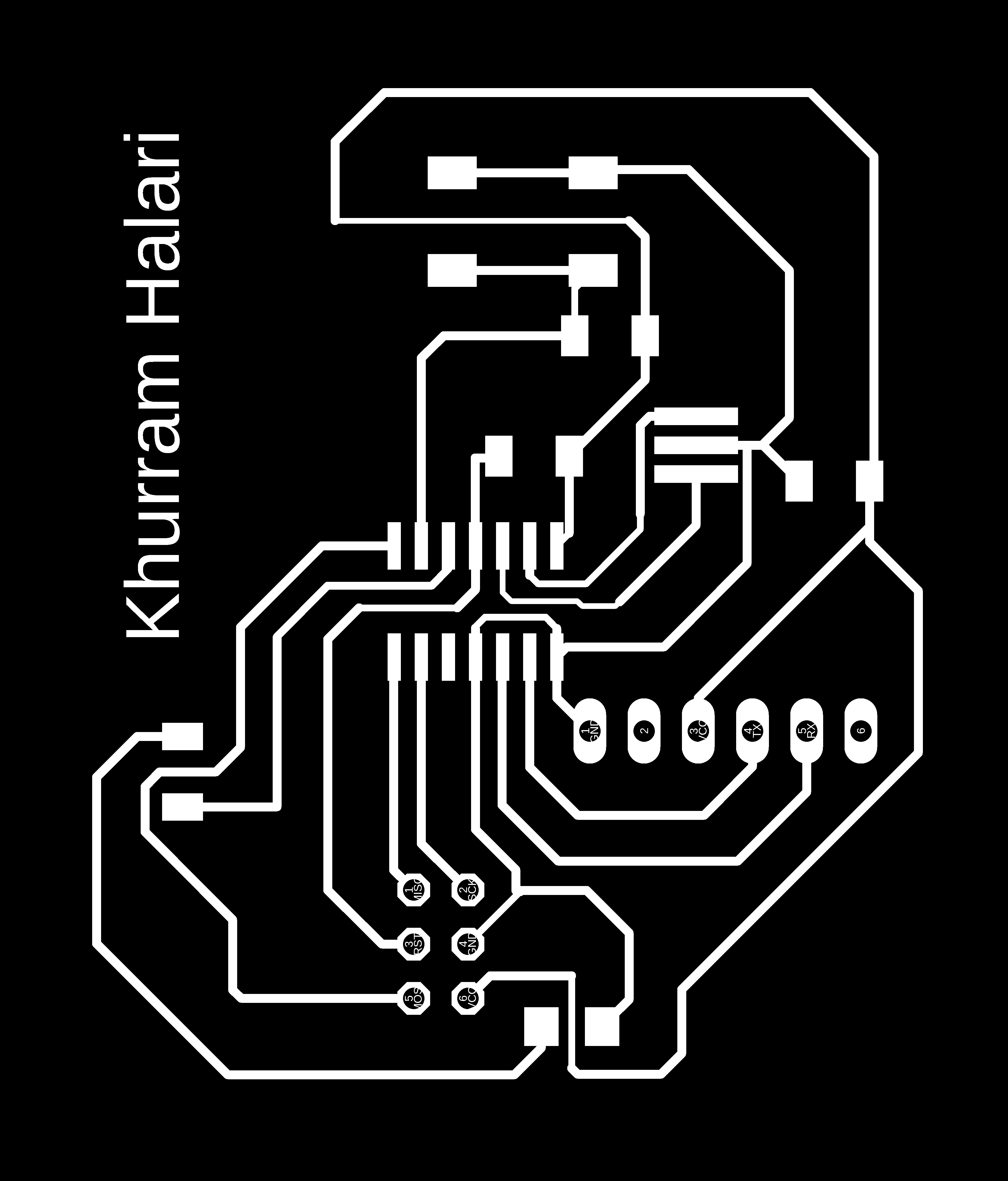
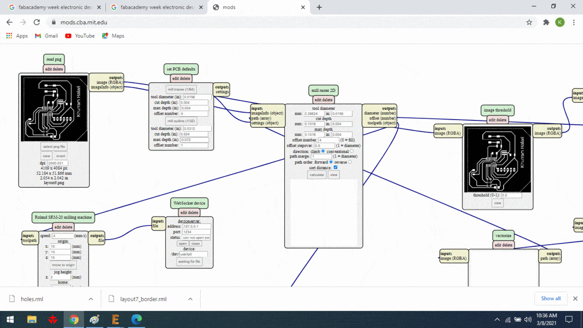
Then I have given the file to mods.cda.mit.edu and generate rml file to mill the board.
Board Problem:
My first design is not working because I have not set the dimension of the circuit border. Due to the border dimension, some layer is removed in my circuit.
I have mill another circuit.
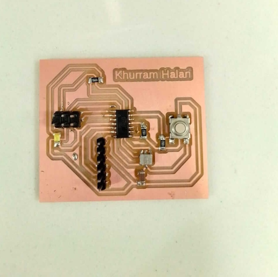
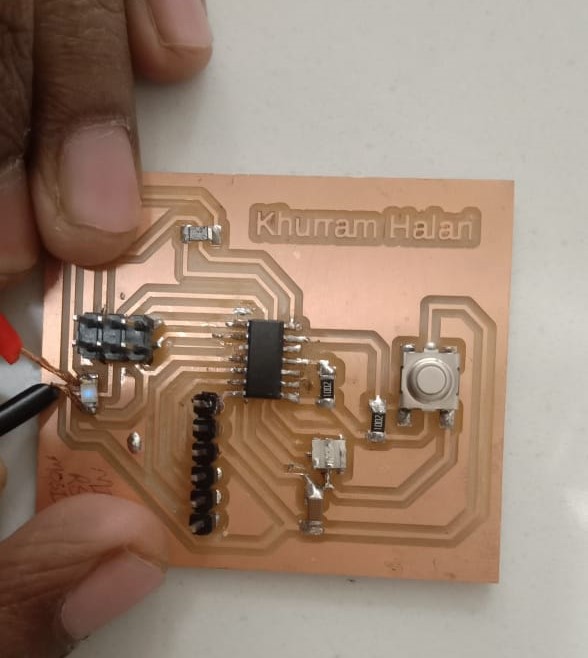
I have completed my new circuit.
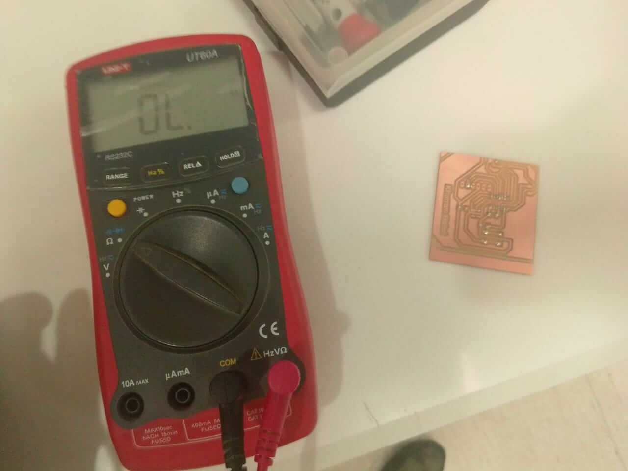
Test circuit continuity.
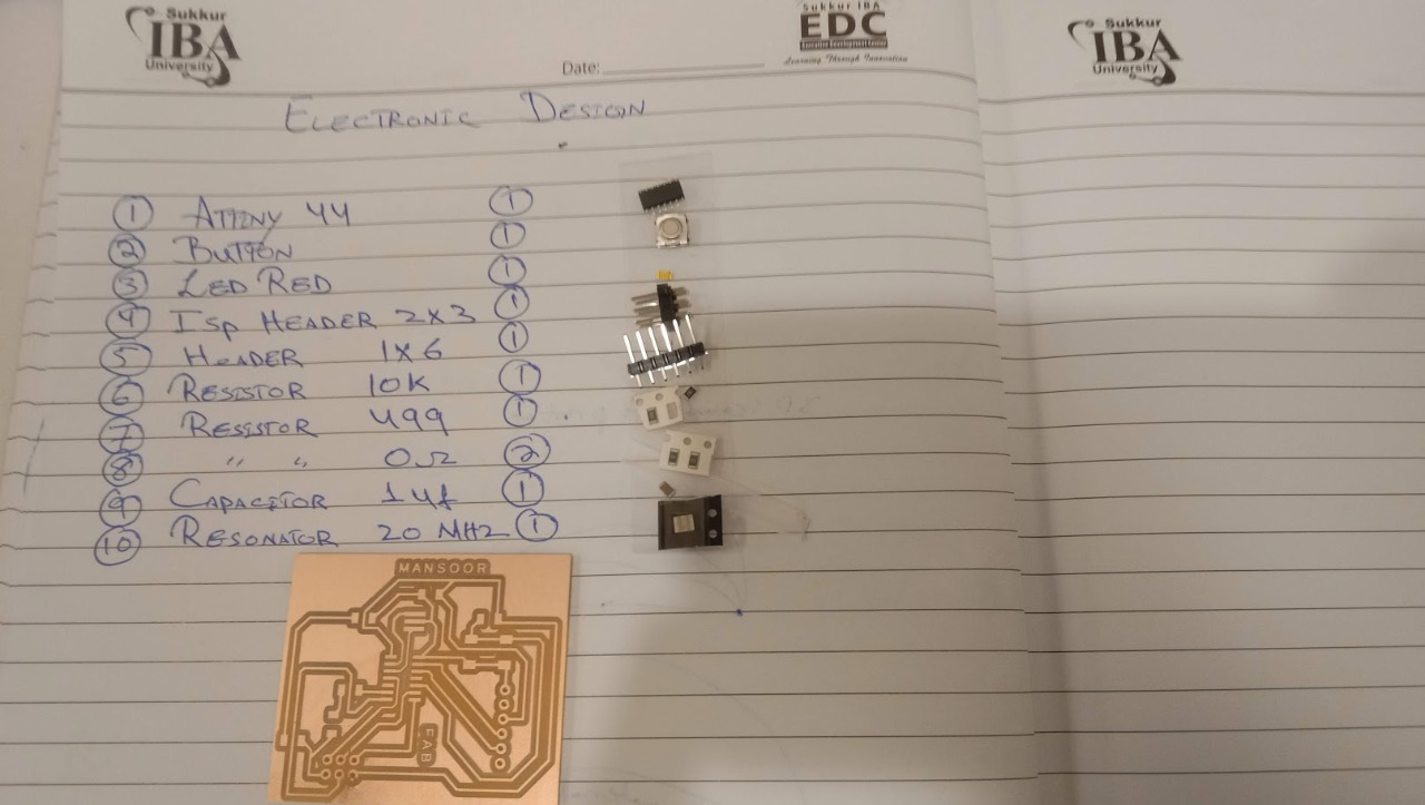
Component List.
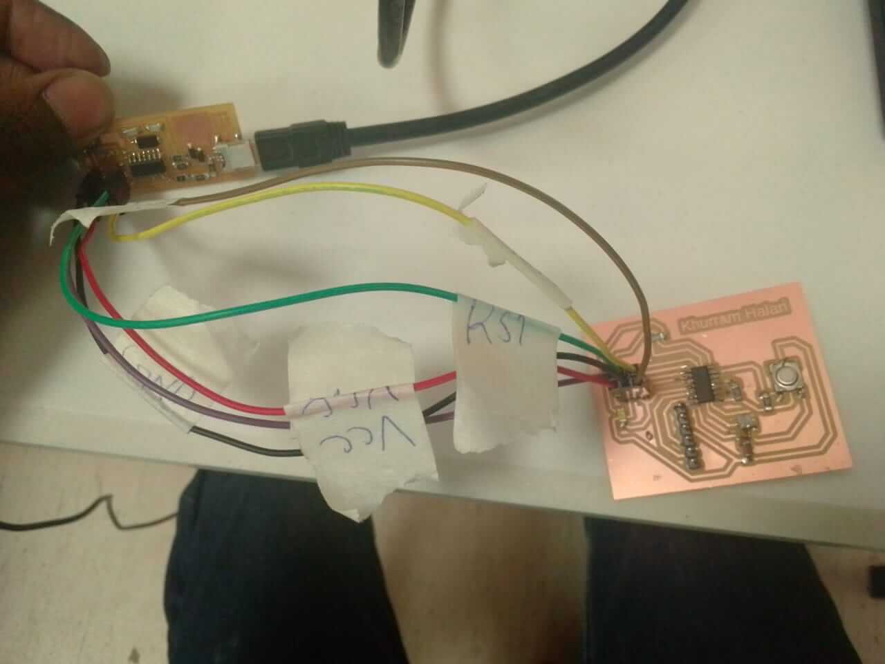
connect ISP board to my hello eco board circuit.
Programming
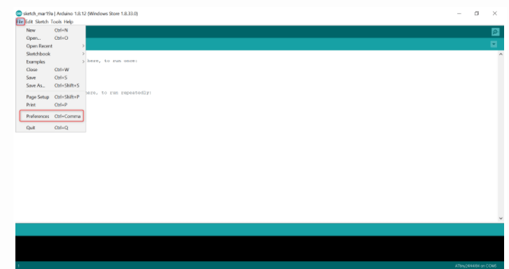
Programming done using Fab ISP board (attiny45) with Arduino software IDE. Steps as following:
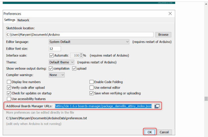
https://raw.githubusercontent.com/damellis/attiny/ide-1.6.x-boards-manager/package_damellis_attiny_index.json
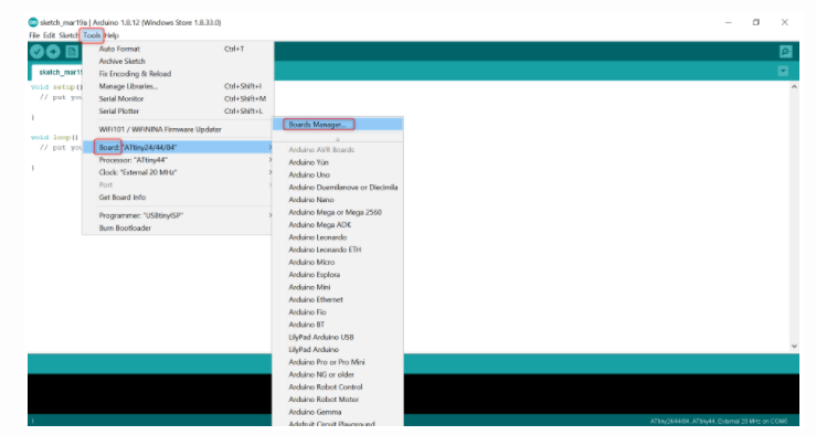
3- From the Tools menu > Borad > Boards Manager.
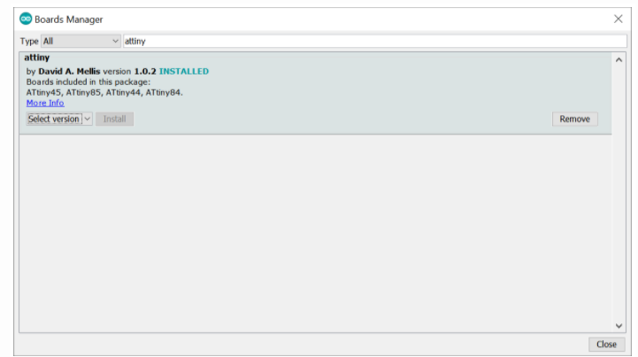
4- Search for attiny and install it.
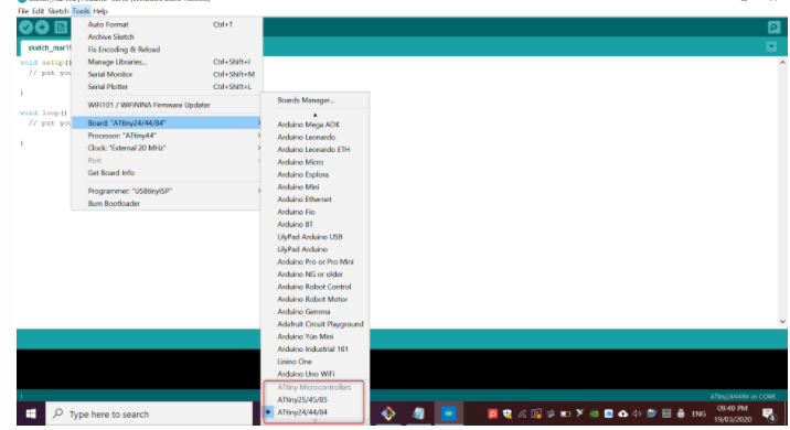
5- ATtiny microcontrollers should be shown in the boards menu.
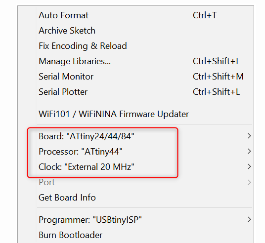
6- Set the following:
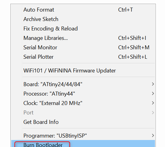
7- Click on Burn Bootloader. When done, you should see this message “Done burning bootloader.”.
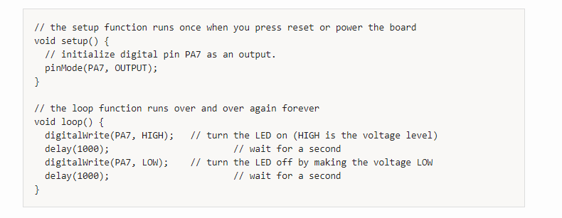
8- Upload a simple blinking LED code to my echo hello-world board.
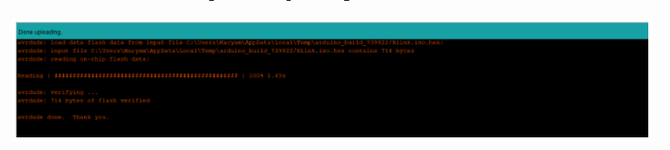
9- You should see this message “Done uploading.”.
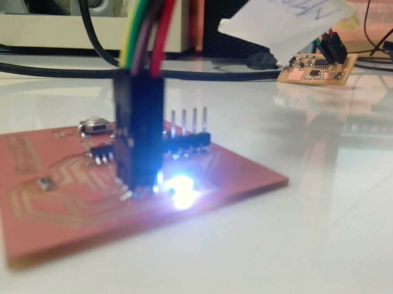
This is my final result.
Microcontroller:
I chose to make my own microcontroller after being inspired by Arduino and having hands-on experience with Atmel family processors and controllers. To do so, I used Atmega 328 microcontrollers and designed the PCB as shown in the photographs.
I began by designing an arduino microcontroller sketch, selecting components from the fab library first, and then finishing the arduino sketch diagram.
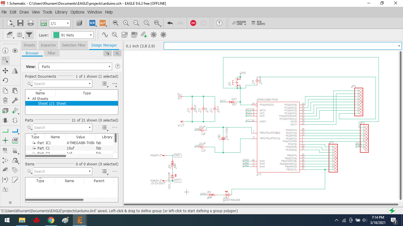
Sketch Diagram
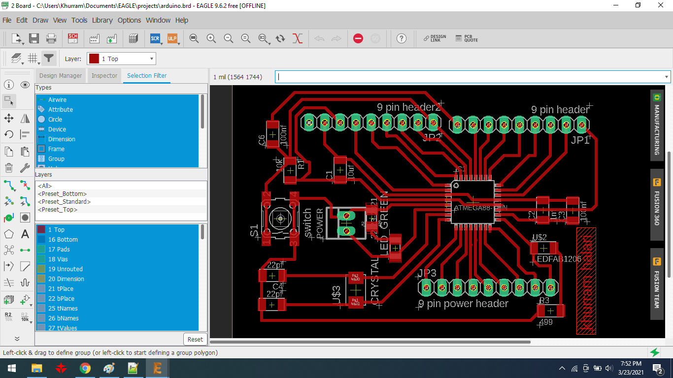
PCB layout of Microcontroller.
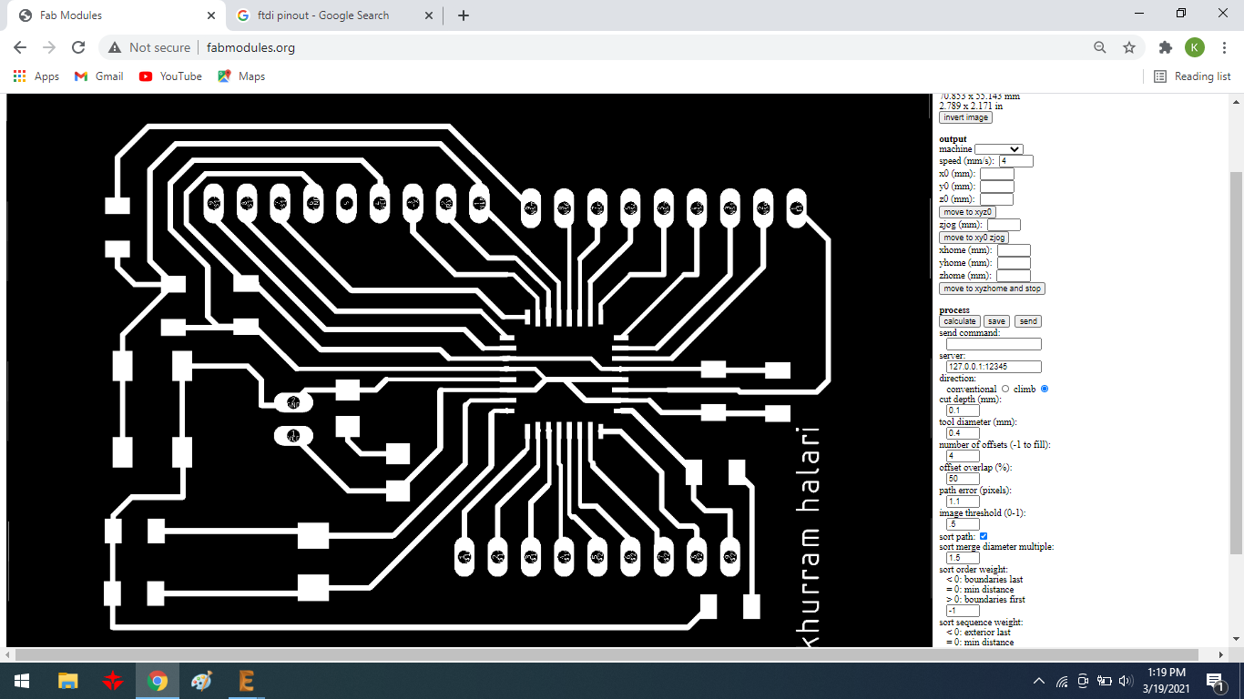
Generating rml file of Microcontroller.
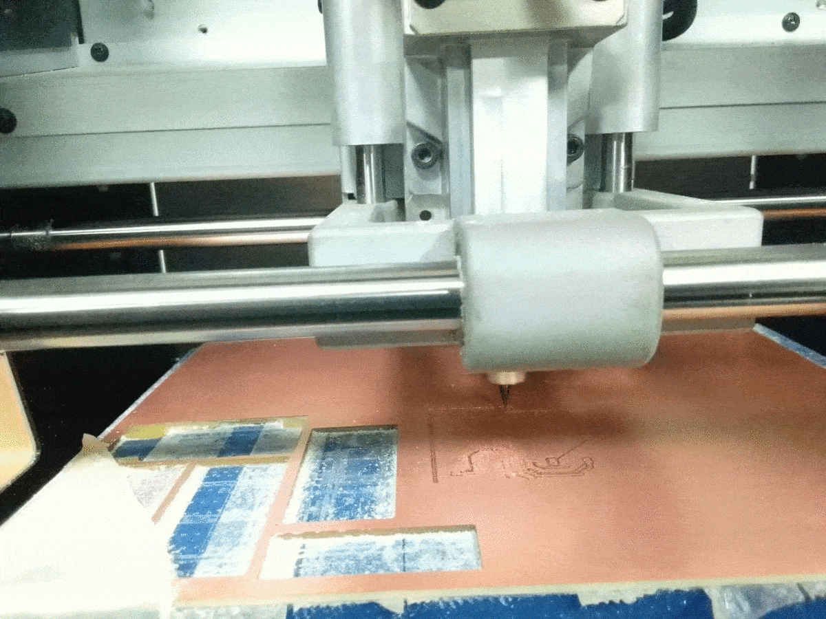
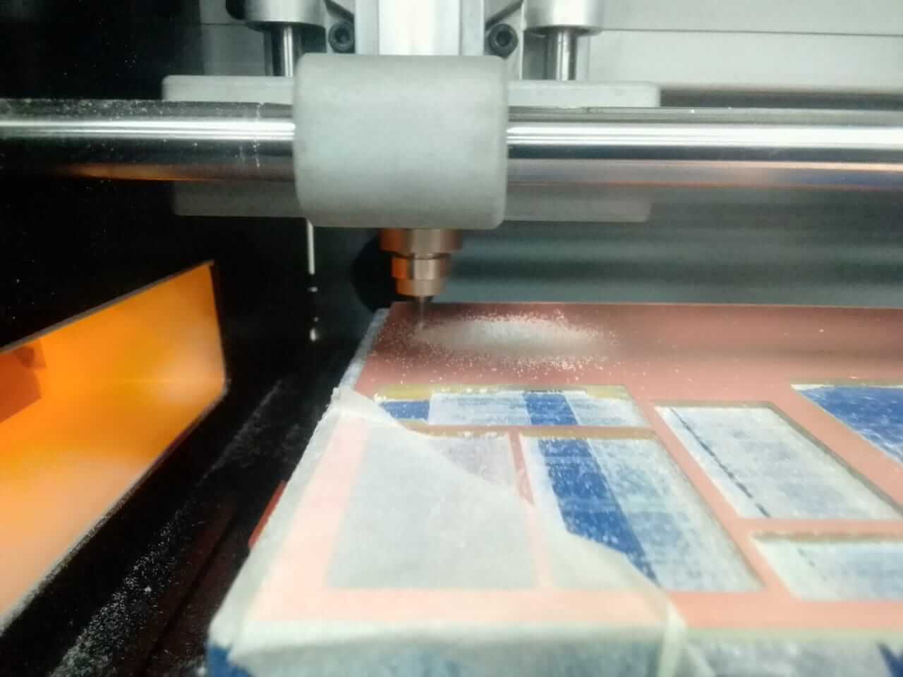
Milling Process:
I gave the rml file to the milling machine for milling the arduino board after designing the circuit in Eagle programmed.
Arduino board milling.
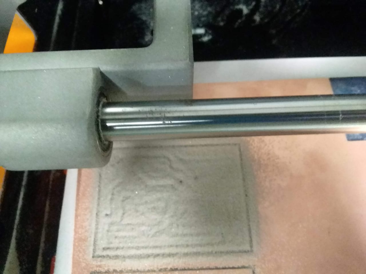
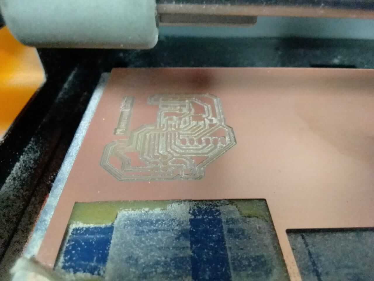
Complete milling process.
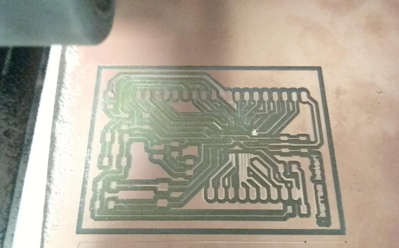
This image shows the final result after the milling process has been completed.
Soldering Process:
After that, I began the soldering process by collecting all of the components and placing them in a safe location before beginning to solder.
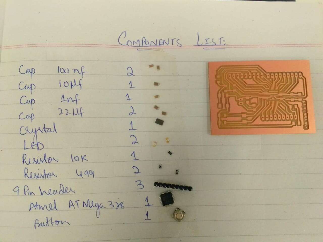
Collect all components.
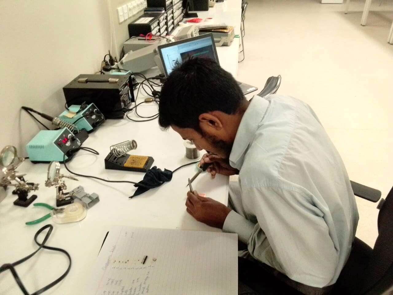
soldering components in microcontroller board.
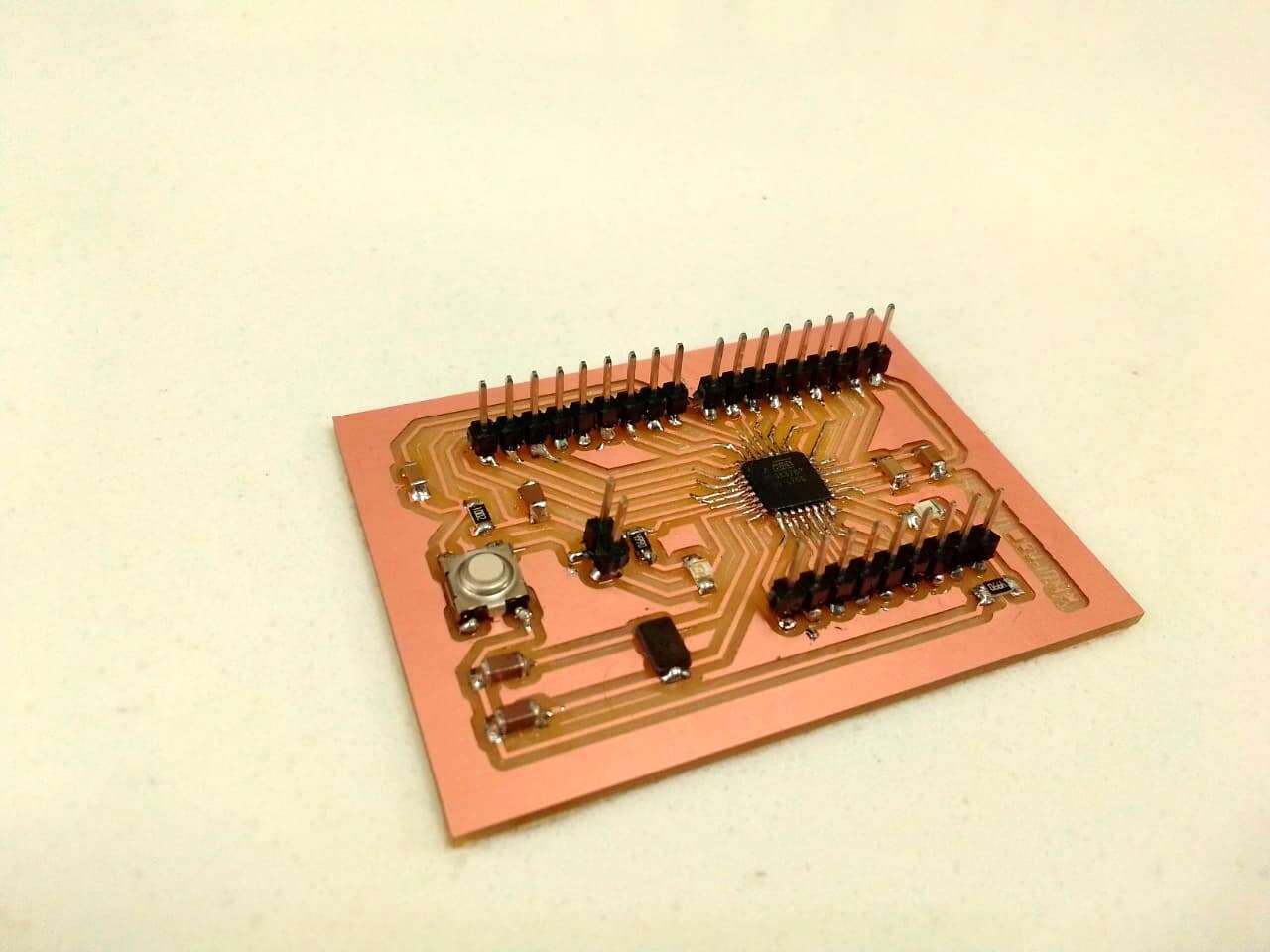
This image show the Final result.
Task:Group assignment:
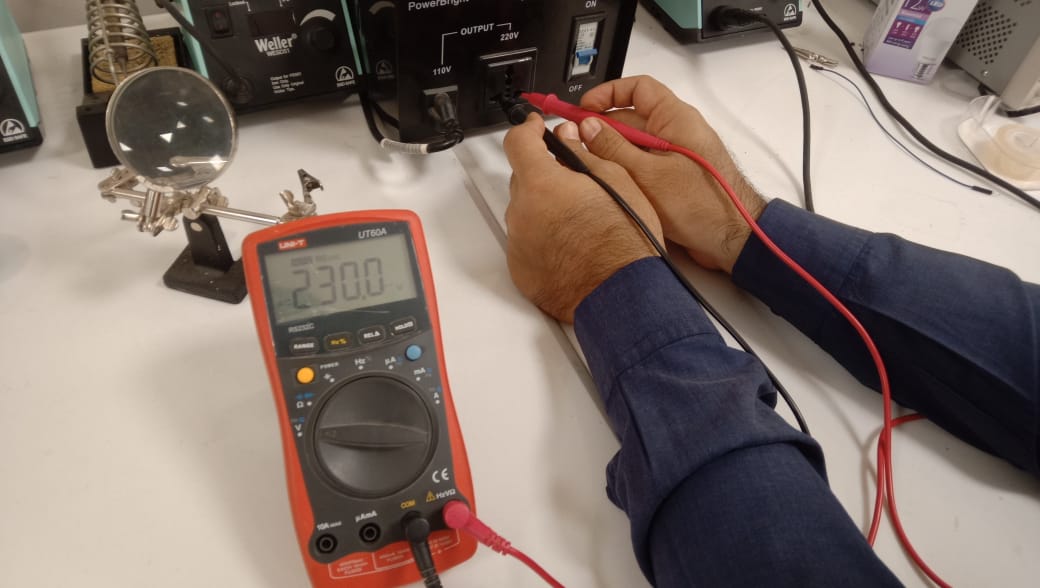
AC Voltage.
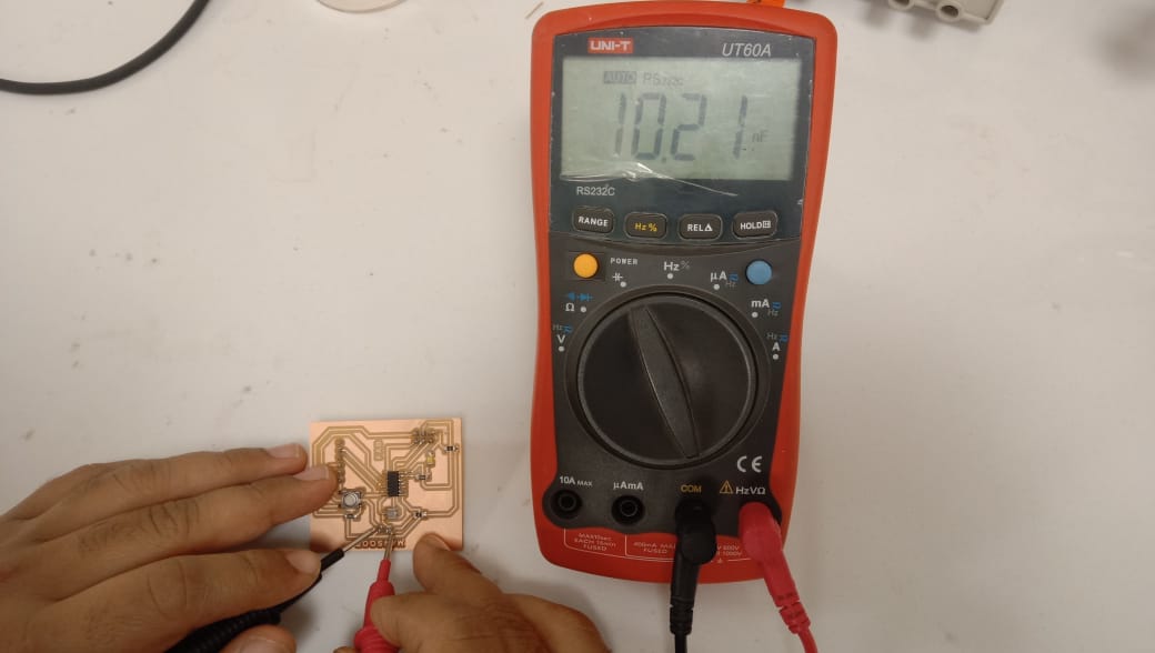
Capacitor value.
Checking of the polarity of led.
"Click here"to download all files of this week