Week 6 : Electronics Design
☛ Group Assignment
☐ 1. Use the test equipment in your lab to observe the operation of a microcontroller circuit board
☛ Individual Assignment
☐ 2. Redraw an echo hello-world board, add (at least) a button and LED (with current-limiting resistor) check the design rules, make it, and test it extra credit: simulate its operation
☛ Electronics basics
☛ Inside the Atoms
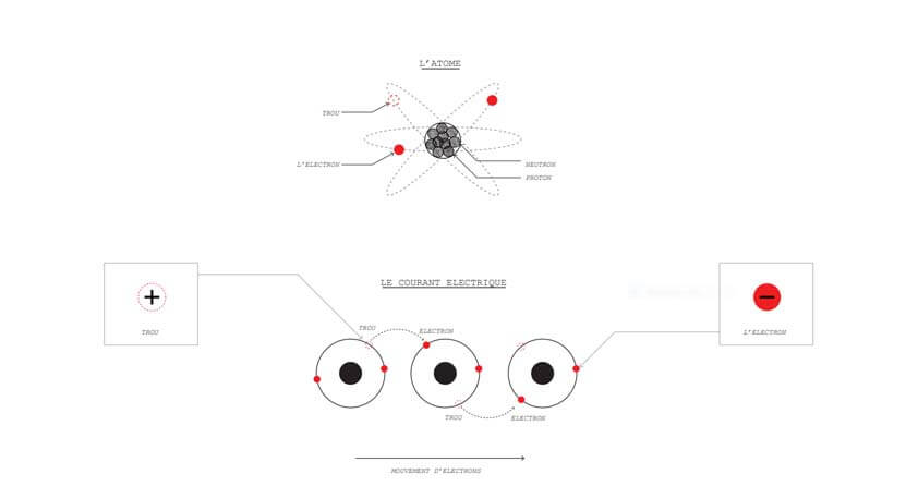
Electronics is about Electricity, more precisely about Atoms and how they are built : Atoms are composed of Protons, Neutrons and Electrons, their behavior regarding their density in a given space, let's say an electronic circuit, creates a flowing charge of electricity. Each atom has a center nucleus in which protons and neutrons are densely packed together; the group of electrons are obiting around the nucleus.
Electrons always carry a negative charge, Protons always carry a positive charge, and Neutrons are neutral. While positive and negative charge are attracted by each other, positive charges repels themselves, and negative charges do the same, this creates a movement in the atoms structures, this movement is called the flow of electric charge. This part is illustrated on the image above, which is extracted from Jonah's presentation on electronics basics. The charge is a measurable property that can be negative or positive.
The concentration of electrons creates tension, which can be measured with a multimeter.
☛ Atoms on the road
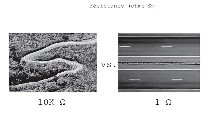
Our instructor, Jonah, has a great metaphor to explain the behavior of the flow of electrons in a circuit. (This image above is extracted from his presentation). In this metaphor the circuit is basically a road for electrons, distance and state of the road (a straight line as an Highway is optimized for a lot traffic, a winding and turing road is not) will have an impact on speed of travel and on the conductivity of electrons.
A closed circuit is the kind of circuit you want to have next to you. A closed circuit allows current to flow, but an open circuit is a dead end for electrons flow.
A short circuit is when a direct connection between two points in a circuit that aren’t supposed to be directly connected occurs. Electric current takes the path of least resistance, so the current will bypass other parallel paths and travel through the direct connection. If a power supply is short out, it sends large amounts of electrical energy from one side of the power supply to the other. With nothing in the circuit to limit the current and absorb the electrical energy. A short circuit can melt the insulation around a wire and may cause a fire.
In the atoms of a conductive material "valence electrons", electrons from the outer ring, are moving from one atom to the other, they're called **free electrons". Some elemental types of atoms are better than others at releasing their electrons.
In an open circuit, free electrons are moving haphazardly so there is no electric flow, whereas, in a power supplied closed circuit free electrons acquire motion from the terminal (-) to the terminal (+) of the generator.
Elements with low conductivity are called **insulators**, they prevent the flow of electrons.
☛ Ohm's Law
- V, Volt, V : Voltage is the difference in charge between two points.
- I, Amp, A : The current is the rate at which charge is flowing.
- R, Ohm, Ω : Resistance is a material's tendency to resist the flow of charge.
The amount of electric current through a metal conductor in a circuit is directly proportional to the voltage impressed across it. Ohm expressed his discovery in the form of a simple equation, describing how voltage, current, and resistance interrelate :
- V = I x R
- I = V/R
- R = V/I
☛ Choosing a resistor for a LED
- Use the datasheet of the component to check its properties
- Use Ohms Law : R = V / I
- Power tension - component tension required / component current use
- 4.3V - 2.1V / 0.02 = 110Ω
- Use the resistor with the closest value
☛ Tools to measure and oserve electric flow
- Multimeter
- Oscilloscope
- Digital Logic analyzer
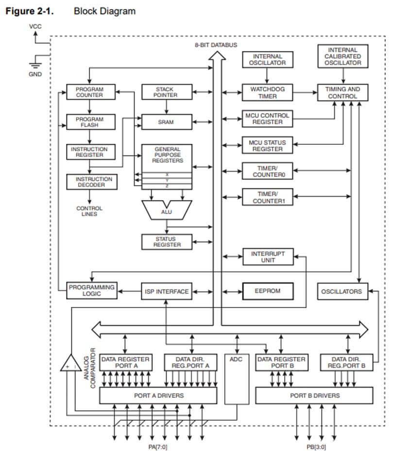
☛ The ATtiny44 Microcontroller
A microprocessor, as the ATtiny44, is a tiny and inexpensive computer which can interact with the physical world.
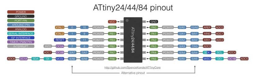
Inside this 8-bit computer :
☛ Making the Hello Board Schematics Circuit
Hi beginner ready to meet Eagle PCB, it warmly welcomes you. Or almost. The interface of Eagle is not intuitive at first sight, and it takes time to get used to manipulation on this software. But its use allows such an empowerment, making our own PCBs, and this is pretty exciting. Well, it will be much more exciting when I will completely understand what I have learned so far, during the Pre Fab Academy, and since it has begun. It is enormous, and it is far away from what I've done before, so it is a lot to process.
Circuits have several "representations", the schematic one, which is a plan, an architecture of components that are linked. Its purpose it to show how it works, how it is structured. Then, there is the 3D circuit on the board, with components linked by traces.
Eagle is composed of two design interfaces, the circuit's schematic and the circuit's board.
☛ Setting up the components libraries
To begin, the first step is to gather the footprints of the components you will use, in our case these components are listed in the fab library, we also installed the Adafruit and Sparkfun libraries. Here isa link to the Sparkfun and Adafruit libraries and a tutorial to install them.
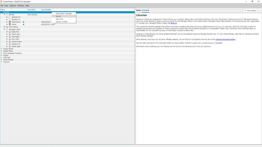
After downloading the libraries in the library folder of Eagle, you have to make sure you allow them to be used in your projects. On the Eagle main page you can Right click on Library > Click "Use All".
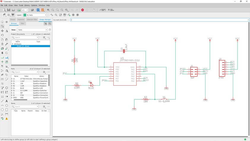
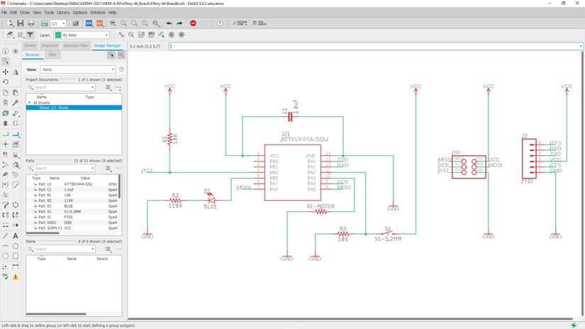
☛ Drawing the Schematics
The schematic circuit is ruled by several conventions to make it understandable for more than one person. These conventions are symbols for each types of components, "concepts" (like GND and VCC you have to add as a "part"), positions (VCC up and GND down), building modules that are linked rather than melting them in the schematics. For instance.
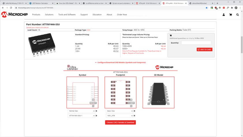
The screenshot below shows where to get the footprints the Attiny44A from Microchip on their website, you can simply download the package composed of the schematics, the footprint and the 3D model, and then install it as a library in Eagle. This part is done by extracting the file in the Eagle folder on your computer, and "use all" libraries from Eagle softwware's home page. Another way to get those footprint would have been to listen more carefuly : there is an Eagle (and KiCad) library composed of all of the Fab Academy inventory.
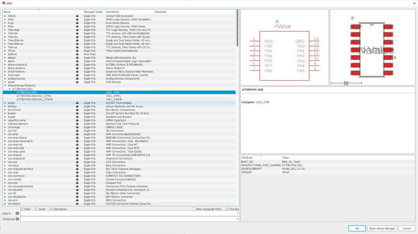
Once the libraries are setted up, you can click on "Add Part" in the left panel and select the components you need one by one.
I added the components I need, I have now to name them, to link them, and to add the GND and VCC symbols that are also parts to add in the schematics.
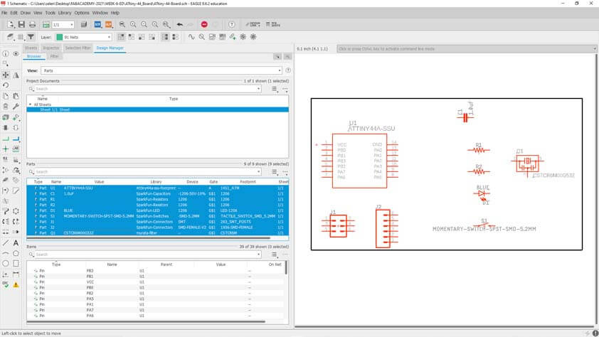
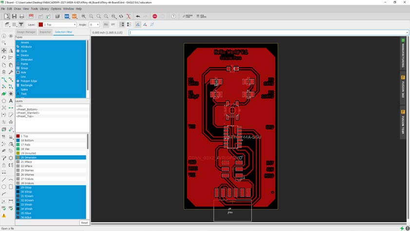
Here is my circuit fot the ATTiny44A Hello World board with a LED and its resistor and a switch button.
☛ Making the Hello Board PCB Circuit
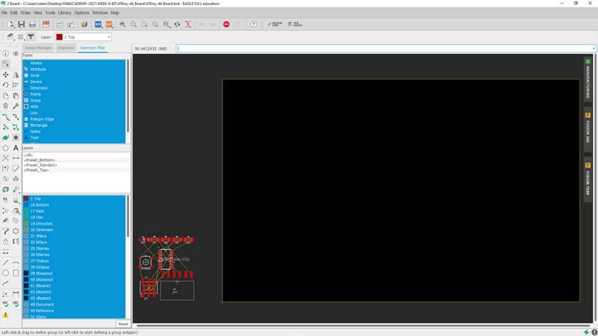
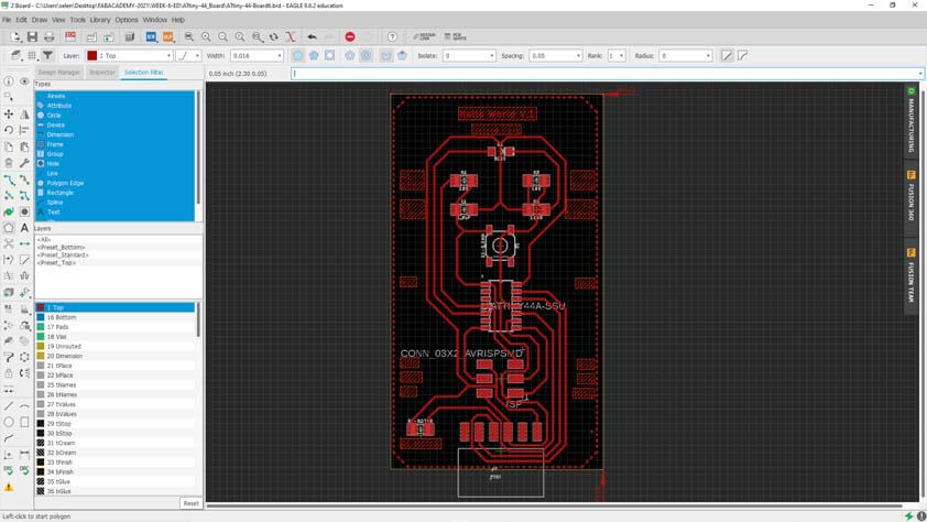
How I learned to use Eagle is to create a Schematics first, not a project, and to create a aborad for the circuit once hte schematics are ready. In the top Icon menu, the fourth one from the left allows to switch from the board to the schematics and from the schematics to the board. When you create it for the first time, it place all the components at the bottom left of a black rectangle, which represents the surface of the board.
Before placing the components it is a good practice to set up the grid layout and most importantly the size of the traces (depending on the production process you will use).
I made several attempts, using the rounded angles traces, and the squared ones. Eagle is very helpful when it comes to link the traces to components. It highlights the pin where you have to go to, but it can be long to find how to link everything in an ordered manner.
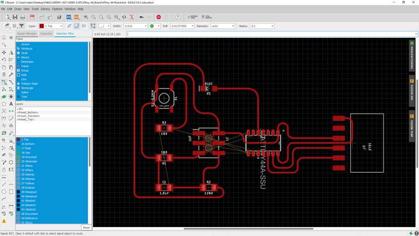
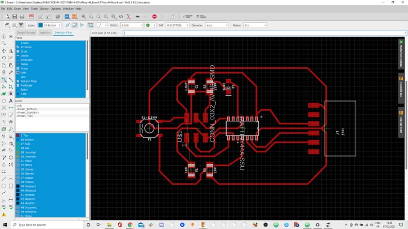
The screenchot below shows the board with all the compoents linked.
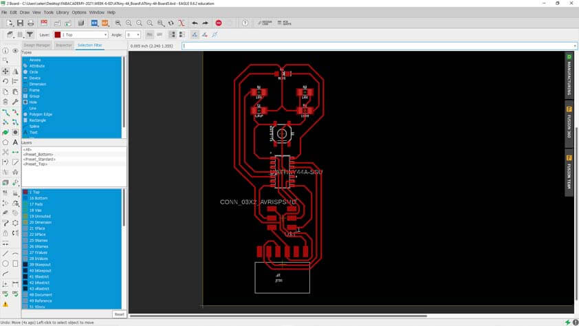
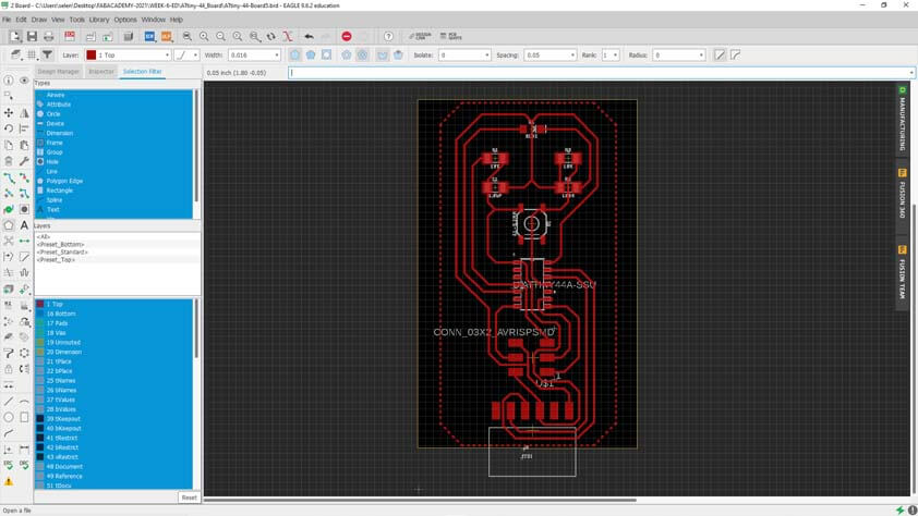
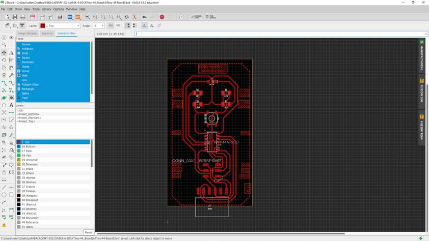
The three images below shows the process of creating the ground plane on the board, this step allows reduces interferences.
First, ccreate a polygon that surrounf your traces, and name it GND. It will produce a border of dots. After this step I chose to add text on my board, it name, and the values and nature of the compoents on it, or of the pins, so it is easier to understand what this board does.
Regarding the ground plane, when you set you can click on "Ratsnest" in the left menu, and this will generate the ground plane.
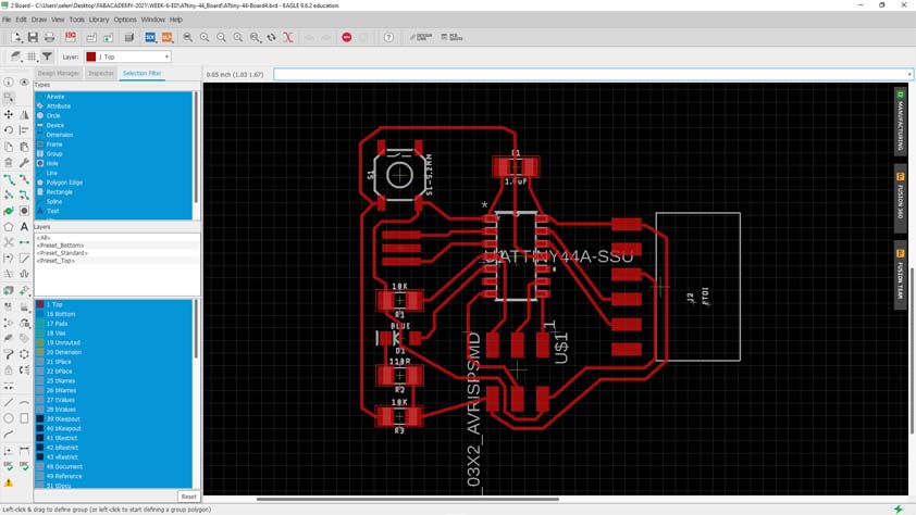
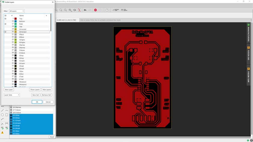
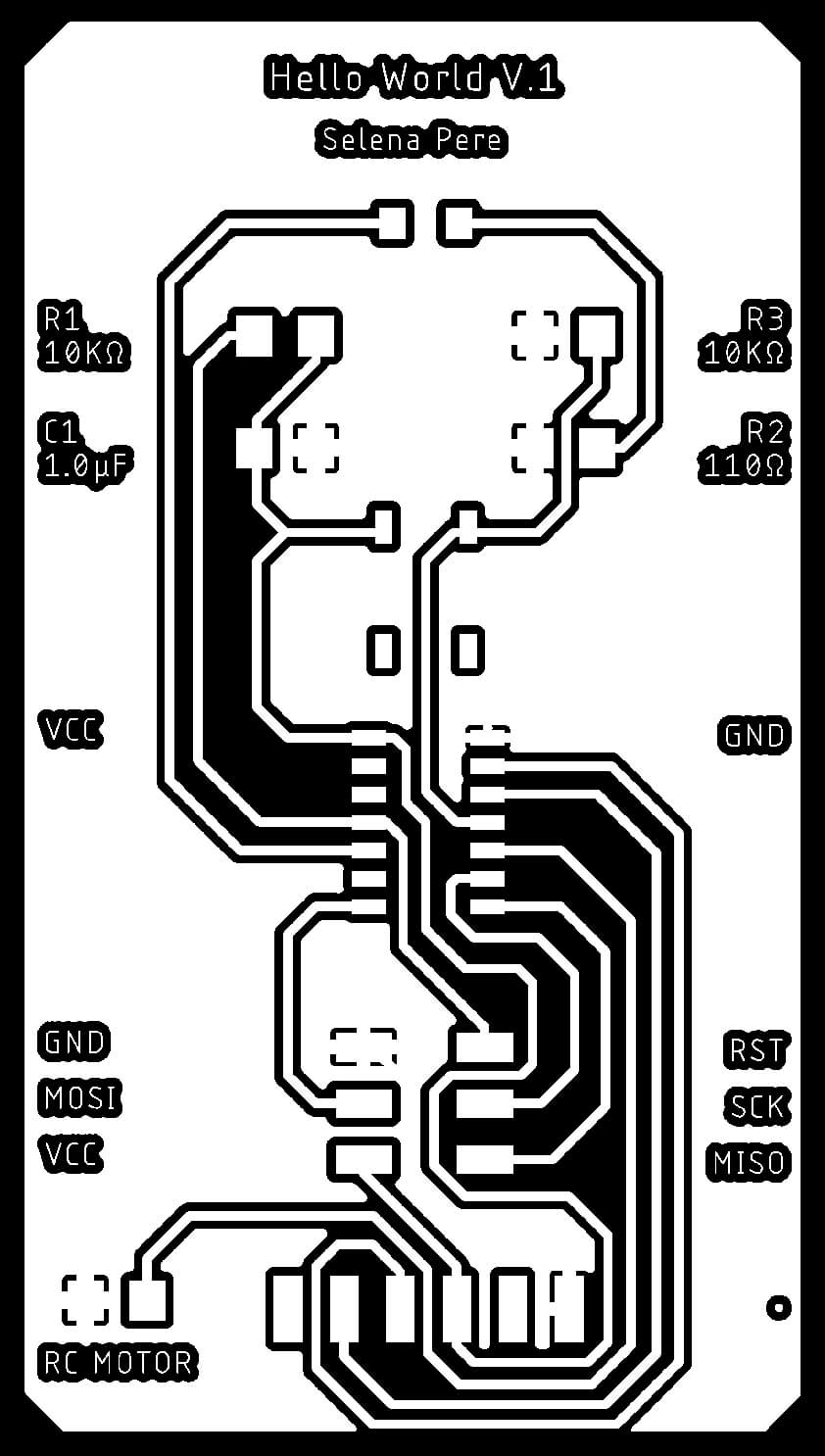
Once the board is ready we can export it, how to dot it :
- Open the layers menu and make visible the "Top", "Pads" and "Dimensions" layers. As we are produce a single-sided board those are the three layers we need.
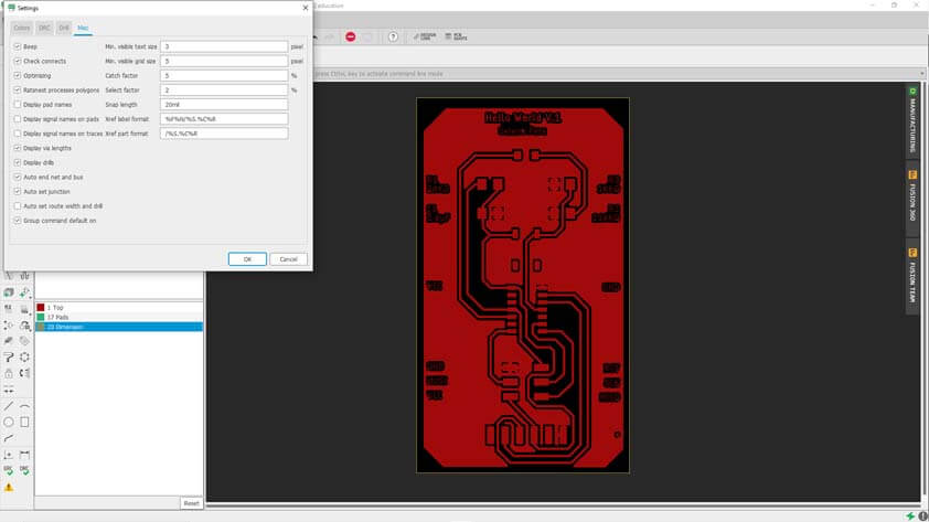
- Go in Options > Settings > Misc and unclick "Display pad names", "Display signal names on pads", and "Display signal names on traces". As we are goinf to export an image, we want ton make sure we gather the right amount of informations.
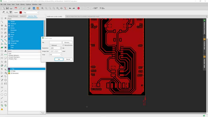
- When 1 and 2 are done you can go in File > Export > Image. It opens a window in which you can identify the file, tick monochrome so the export is white and black, if not clicked the image exported will be red and black. The resolution has to be set to the higher level, as we are going to raster this image with a laser cutter machine. And click Ok to finally export the image.
☛ Modifying the Circuit
I decided to try to add an Rc motor so it could switch on the light when blowing on it, to reproduce the basis of my controller for the final project. To do so I added a Generic resistor in my schematics, with no value, as I just want to use the footprint to solder pins on which I will be able to link the RC motor. I chose an analog pin to plug it in, I searched in the microcontroller datasheet and the 10th pin of the ATTiny44A is an analog one.
I placed the footprint on my board, grounded and then exported it.
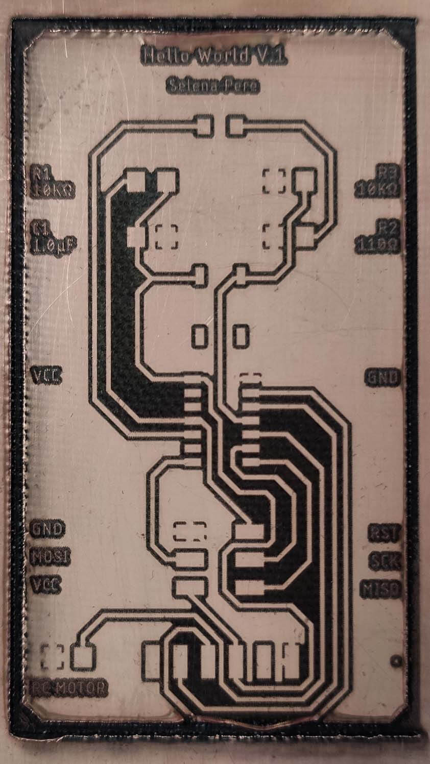
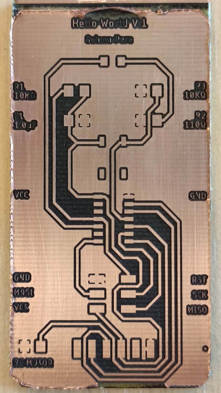
Here are the traces and outline of this board. These images are compressed (no 12000 dpi here). The link to download these files is at the end of the page.
These two attempts were pretty disappointing. Beyond the lack of time, I think I forgot changing the focus when going from Fiber laser to Co2 laser, so the result on the left below shows that. On the right, I thought I entered the right parameters, but at the end the board wasn't cutted at all, there was only a trace and I had to cut it using a cutter. Its thickness and my frustrated sweetness achieved to destroy its borders. I will solder this board at least to test if the circuit is functionnal before giving it another try.
UPDATE : The seconde board below wasn't totally cutted because I did not chose the right thickness of FR-4 PCB, it was too thick.
I soldered it to verify that it is working and I discovered that soldering on a ground plane is very difficult, the solder would not adhere to the board. This would have to be confirmed tbut I think this is because it is a plane, and not just a pad, it takes longer to heat, and it is hard to heat it as much as the component : the heat has to propagate in the whole plane to gain in temperature. I produced cold solderings, I will no use a ground plane for my next prototype.
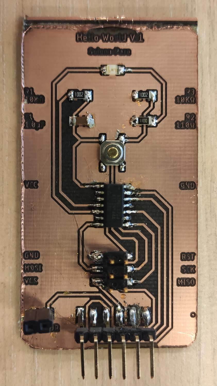
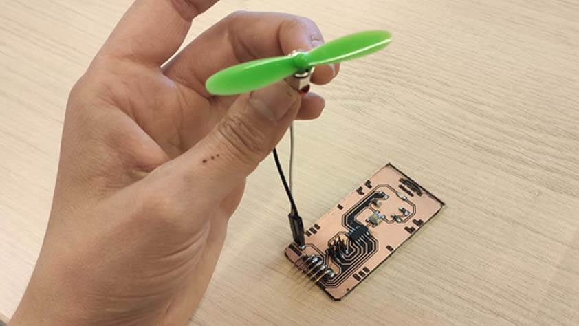
I soldered two pin header on my resistor footprint and I could plug the RC motor on it. The next step is to test if it works.
Direct link to my zipped files from this week. Eagle files + PNG traces and outline