Week 4 : Electronics Production
☛ Group Assignment
☐ 1. Characterize the design rules for your PCB production process
☛ Individual Assignment
☐ 2. Make an in-circuit programmer by milling and stuffing the PCB, test it, then optionally try other PCB processes
▸ Making a PCB using the lasercutter machine
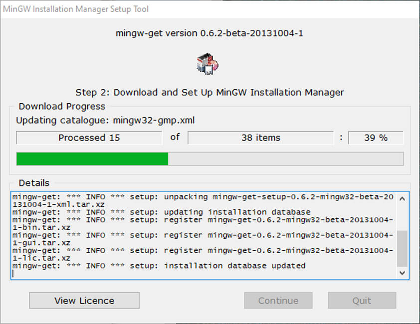
This week Jonah taught us to produce a PCB using the laser cutting machine, and to solder SMD components. We followed a tutorial to make an in-circuit programmer and set up an environment were we could program it.
▸ Group assignment
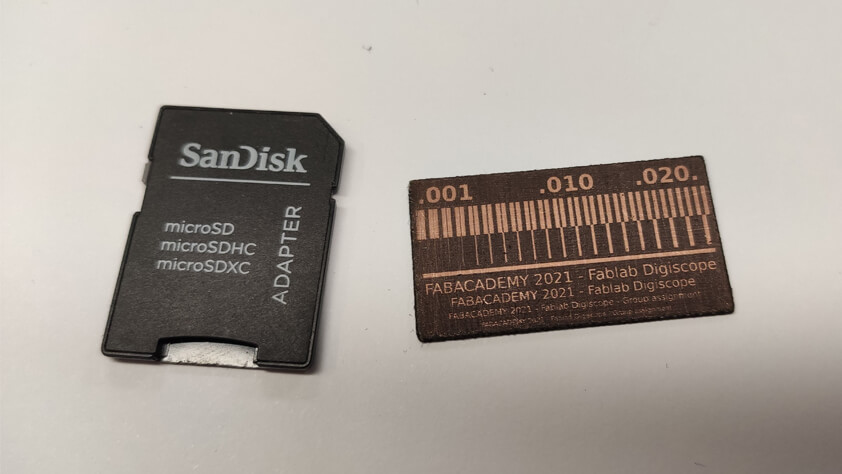
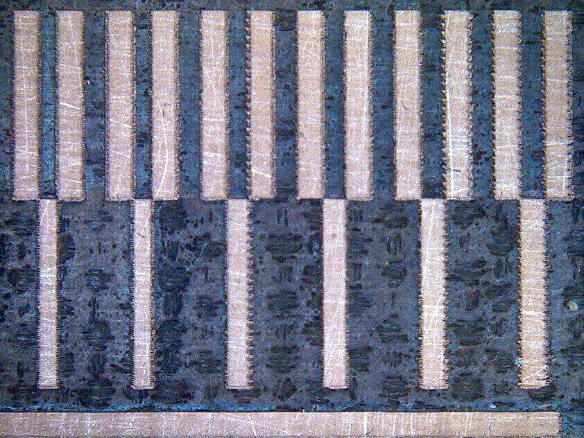
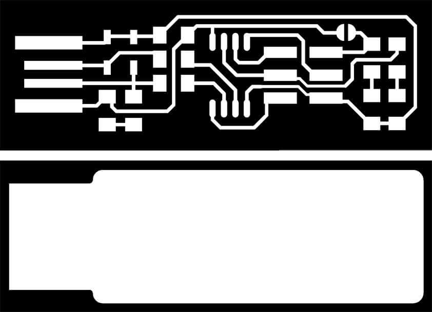
Distance between traces and the size of the tyniest traces our tool can produce efficiently is an important parameter to know ot make a working PCB. As a group assignment, Ambroise modified the traces milling test pattern and added text in different sizes in order to evaluate the precision we could have using the Epilog Fusion M2 40 laser cutting machine. This is a test patter for milling processes but the result seems satisfying but the focus might not have been precise enough as the glass fiber under the copper layer is "coppered-colored".
Nevertheless 16 traces on 20 are good, and up to 18 "between traces" spaces seems to be ok too. The text in a small size are too damaged to be read. Also, we have to admit that the cleaning process of the board may damage traces as we rub the pcb to take off the burnt layer : Straight lines are easier to keep than angles and it has to be done smoothier when working on a more detailed project.
We made a second try using Ambroise file, with a better focus on the material.
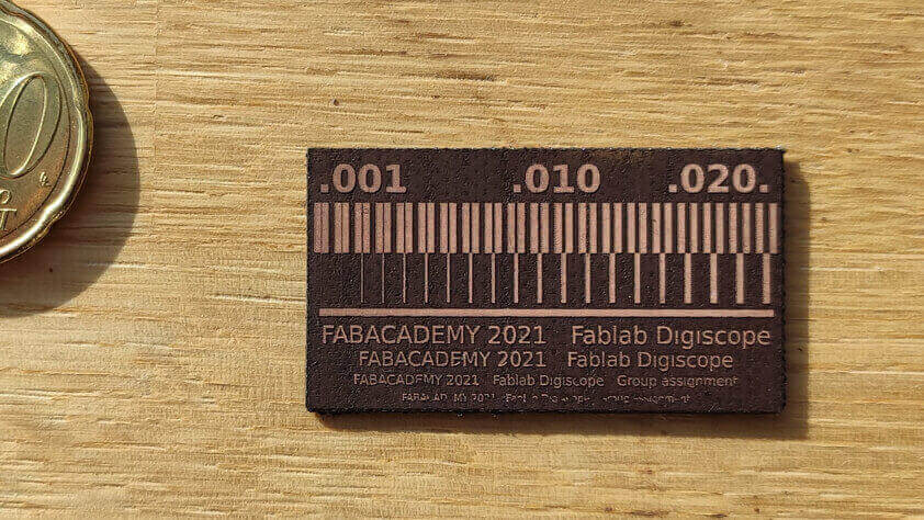
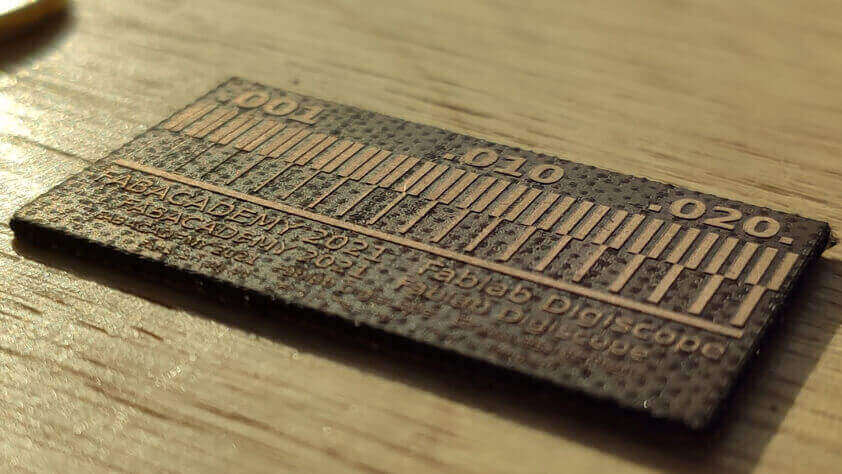
The tiniest and usable trace we can produce on the Epilog Fusion M2 40 is 0.4mm. But our PCB production practice is also determined by the components we have : the Fablab Digiscope uses mostly 1206 components, it is solderable and also, it allows to use components to jump traces on the board.
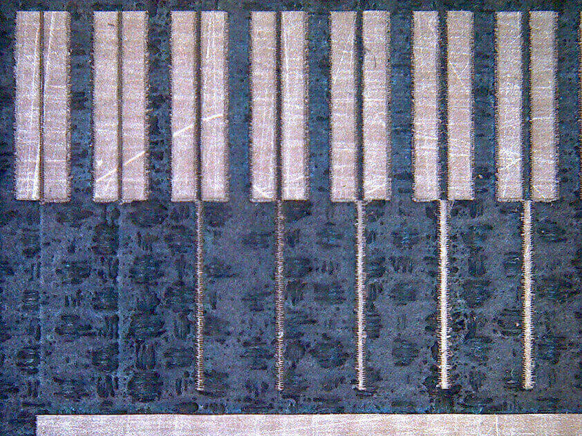
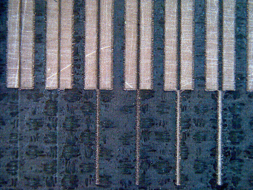
Here I tried to zoom more on the calibration test, and we can clearly see the pixels all along the lines.
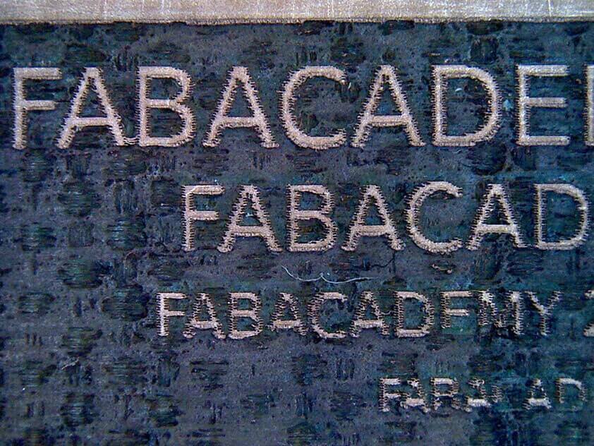
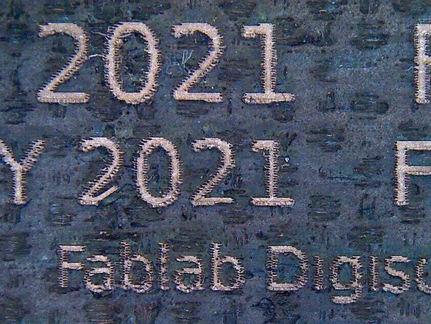
Here is a capture of the text part, we can also see te pixels on the outline of each letter. On the second image we can see that on the second "2021" the 2 is damaged, the traces has been damaged during the cleaning process (sorry traces) - on the first "2021", between the 2 and the 0, on the picture we can see a short-to-be - This is why the cleaning process and the microscopic check are so important. This is not a PCB board but if it was, you totally would like to avoid this copper powder between you traces.
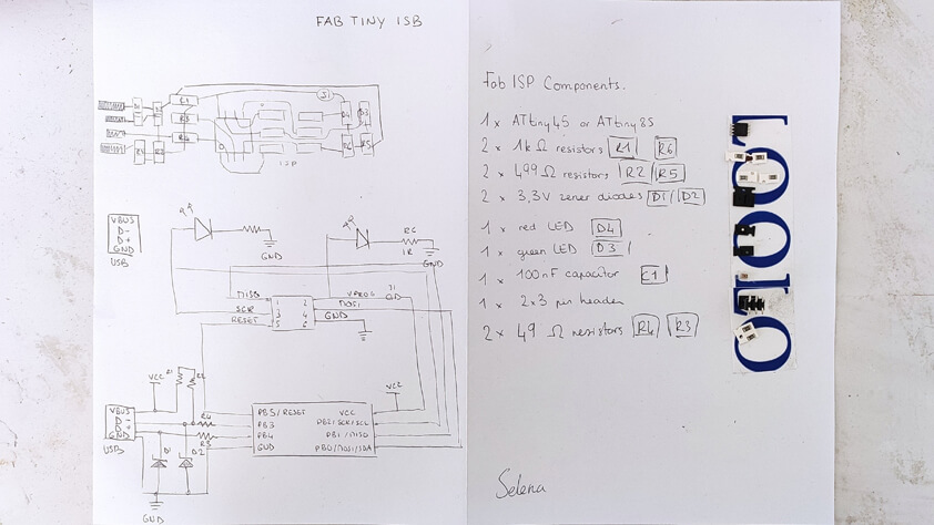
▸ The FabTinyIsp fabrication
To produce our in-circuit programmer we are following this tutorial to build the FabtinyIsp.
In-System programming is a sort of communication process allowing to program and reprogram microcontrollers that are already soldered to a board.
To start we have to download the PNG files to get the board traces and outline, from the tutorial above. Then we can go foward the steps to make it :
- Preparing the FR4 PCB
- Preparing the files
- Fiber laser engraving
- CO² laser cutting
- Cleaning the board
- Using a microscope to check the board
- Soldering the board
▸ Preparing the FR-4 PCB
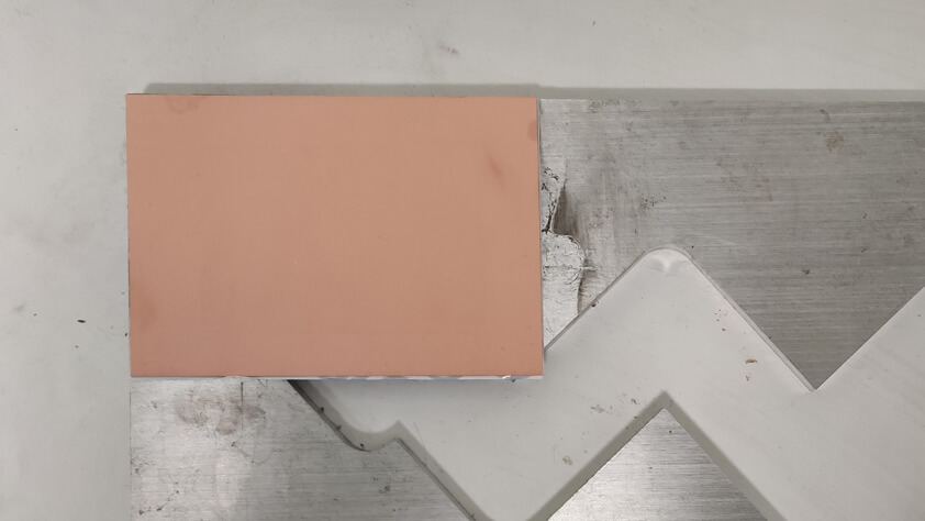
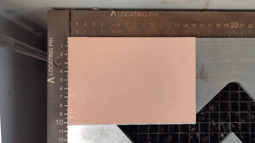
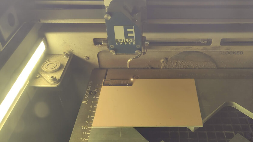
FR-4 PCB is a composite material composed of woven fiberglass with an epoxy resin binder that is flame resistant, and a layer of thin copper foil on one side. We used double-sided tape to fix it to a thick steel plate so there is less risks that the PCB moves, even a little bit, during the laser cutting process. Then we can put all of it on the machine's bed.
▸ Preparing the files
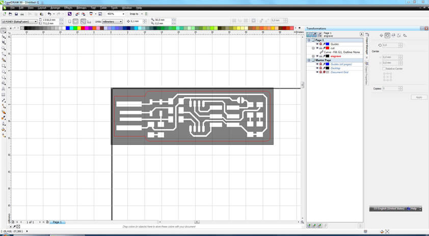
We imported our PNG files in Corel Draw and put the traces file and the outline file in different layers so we can use it one at a time. We are going to use the fiber laser fisrt, to engrave the copper layer of the board and remove it. Then we will use the CO² laser to cut through th FR-4 layer. Wavelengths of these two lasers are different, the fiber one can't go through FR-4, and CO² wouldn't engrave coper. It also means that we have to modify the focus and parameters of the machine between those two steps.
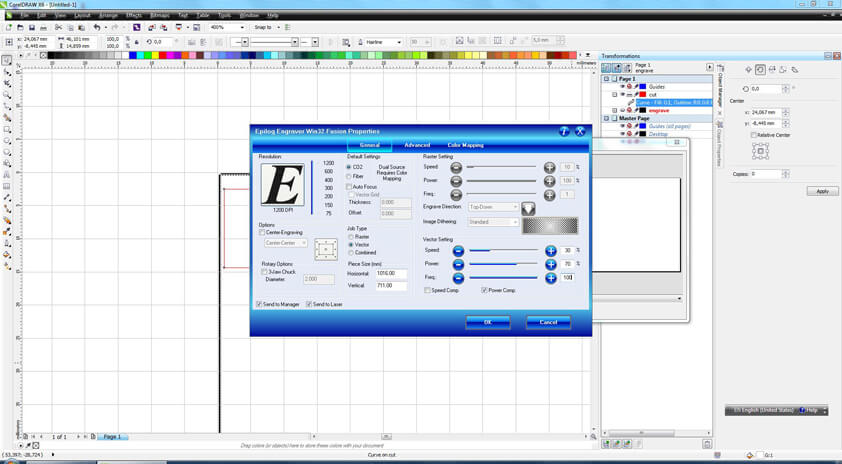
▸ Fiber laser engraving
So, we use the fiber laser first and use the tool to focus it on our material's surface.
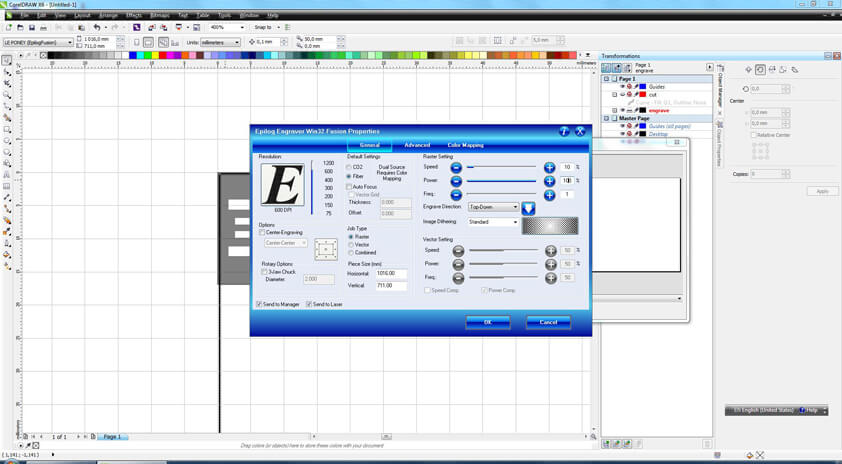
Then we enter our parameters in Corel Draw :
- We are engraving pixels, so have to adjust the resolution in dpi according to our file
- Select the Fiber laser
- Select the Raster Job type
- Enter the Raster settings : 10 Speed, 100 Power, 1 Frequency
- Verify that all of these parameters are set correctly, then Ok, Apply and Print.
- Verify that all of the focus and origin of the machine are set correctly, that the ventilators are on, then you can start the job.
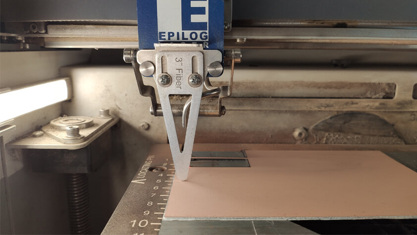
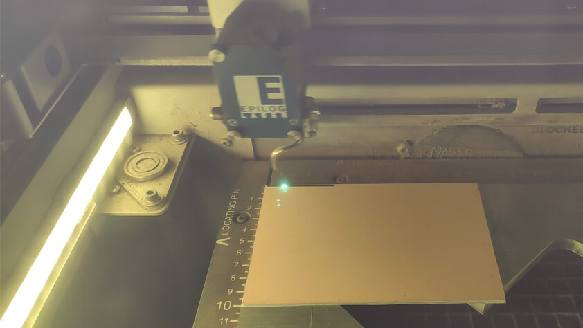
To recognize a good focus when rastering copper, the green colored light at the surface of the material is a good indicator.
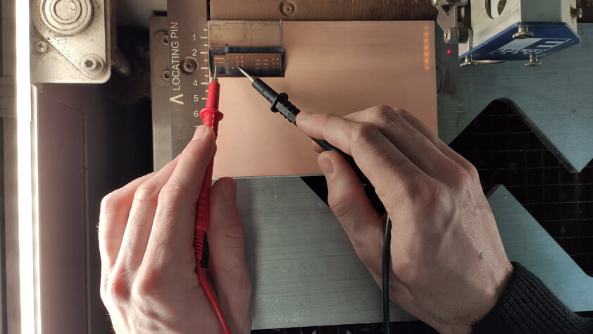
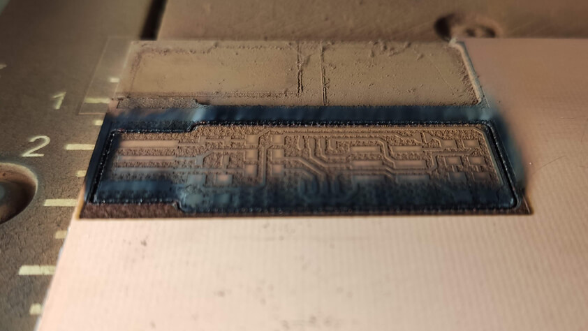
The job lasted five minutes and a few seconds, at the end of it we can use the multimeter to check is the copper is sufficiently removed between the traces. If it is not the job can be restarted - it has to be done before moving the PCB plate from the laser cutter's bed.
▸ CO² laser cutting
Once the board is engraved we have to change the laser we are using and the parameters to work with the CO² laser in order to cut vectors this time. We can select our second layer in Corel Draw (don't forget to click or unclick the printer icon in the layers, so it can actually be printed). Then we modify the parameters :
- Select the CO² laser
- Select the Vector Job type
- Enter the Vector settings to cut through FR-4 : 30 Speed, 70 Power, 100 Frequency
- Verify that all of these are set correctly, then Ok, Apply and Print.
- Verify that all of the focus and origin of the machine are set correctly, that the ventilators are on, then you can start the job.
▸ Cleaning the board
This part is important because the fiber engraving produces "copper powder" that could create shorts on our board. To clean the board we are going to use Isopropanol : We have to use a mask, gloves and protection glasses to do so. The process is to put isopropanol on a cloth and to rub the board with it. It has to be done efficiently, so that the burnt layer is removed, but gently enough so we don't damage our traces.
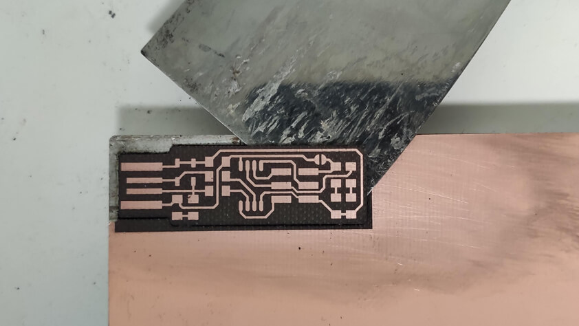
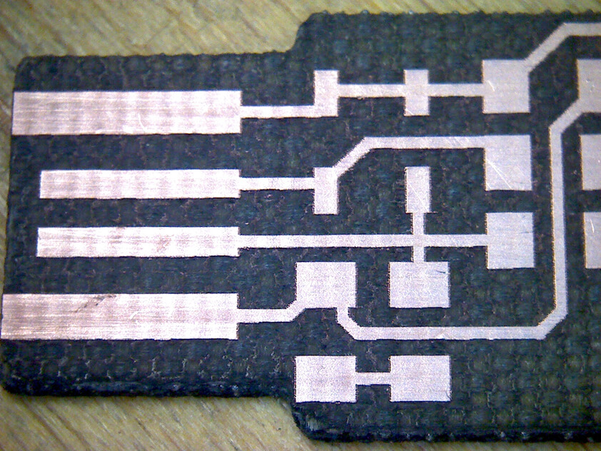
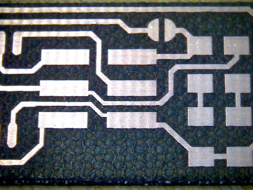
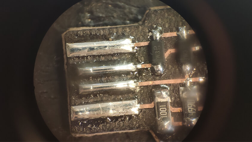
▸ Using a microscope to check the board
Using the microscope allows us to check the board and see if the dust/burnt is well removed, if there is no apparent risks of shorts. Just a detail but using the microscope we can clearly see that the fiberglass is woven too.
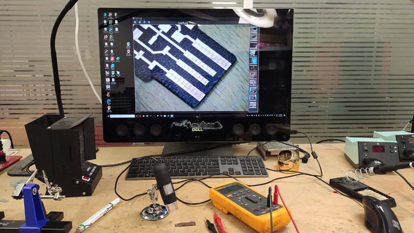
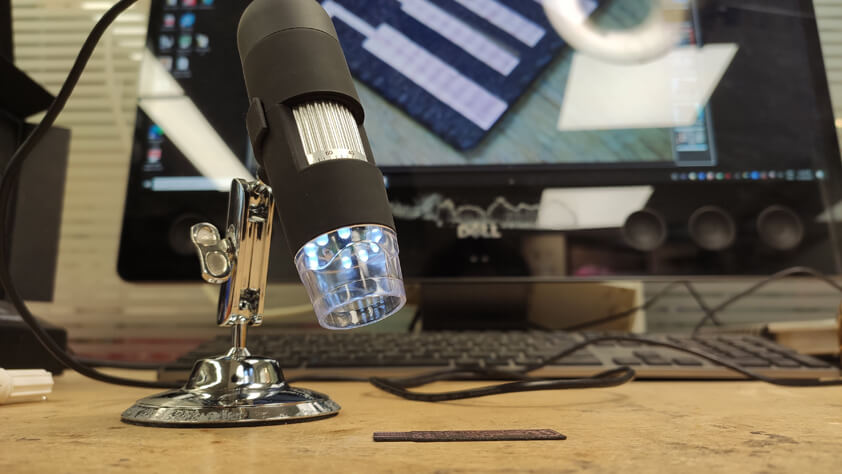
The digital microscope were a using above, and the microscopic view below.
▸ Soldering tiny components (or trying to)
- Soldering basics
- Get your components and schematics ready
- Soldering the FabTiny ISP
▸ Soldering basics
How to solder :
- Tin the soldering iron with solder, it has to be silvery and clean before starting
- Use a sponge to clean the iron
- Heat both oart to solder, so they are at the same temperature and the heat can flow easily
- Approach solder wire
- Remover solder wire, then the Iron
▸ Get your components and schematics ready
Before soldering our board we are gathering our components, using paper and double-sided tape so we can identify those tiny things later.
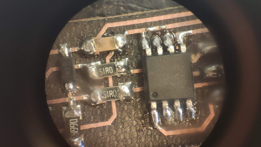
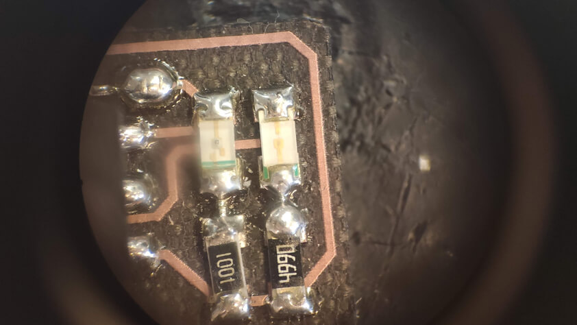
▸ Soldering the FabTiny ISP
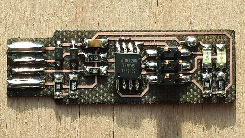
To solder on a board it is important to begin by the components from the center to the outside of the board. It is also better to begin by the most complicated component to solder, in our case it is the ATtiny45 microcontroller.
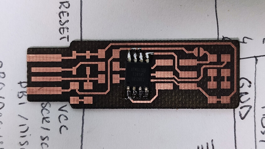
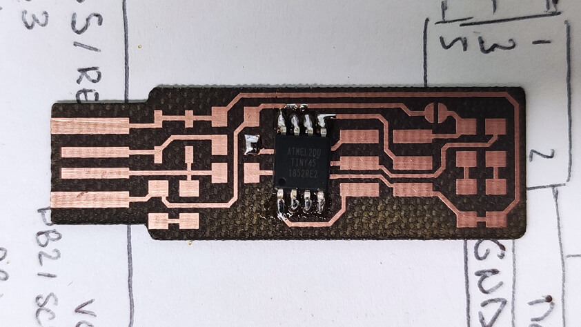
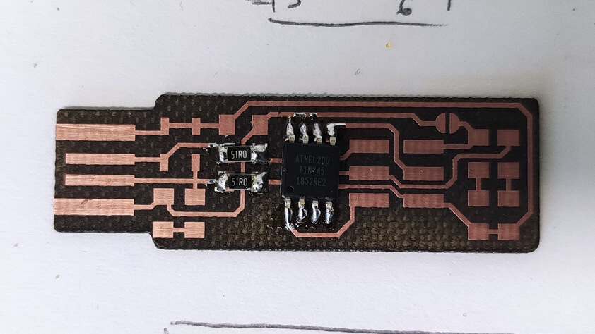
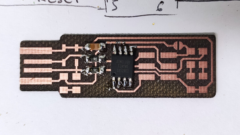
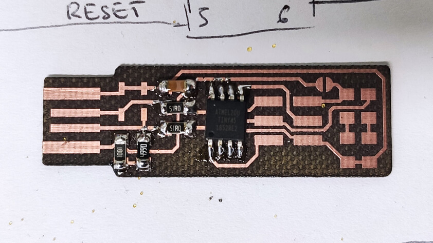
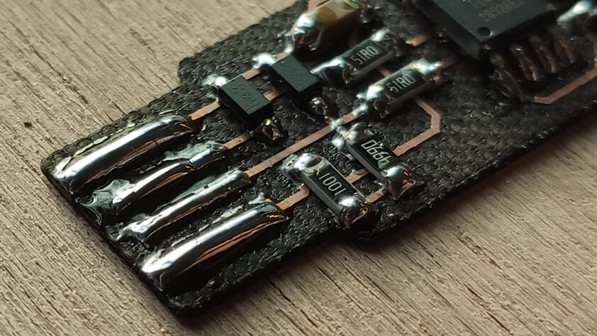
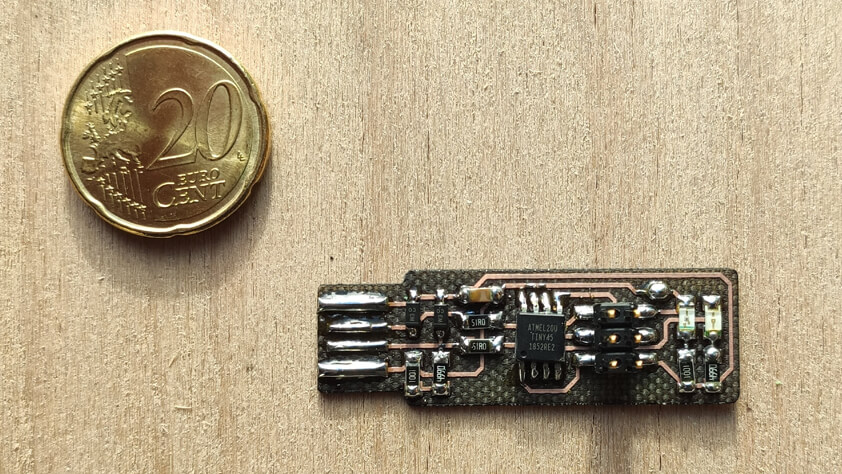
Here are photos of the board with all the compoents soldered on it. The usb traces and the jumper are missing. (I forgot them)
I don't know if it is perfectly smooth, but the sun makes it shiny.
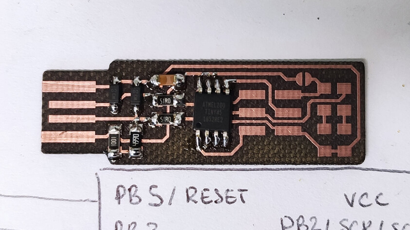
Here are pictures of the board when using the analog microscope.
▸ Before programming : Software installation
Again, this step was made following the FabtinyIsp and this part particularly, regarding the environment set up on Windows.
▸ (not) Setting up the development environment on Windows 10
Before the Fab Academy I was an Adobe user on a computer and that only had to double-click an exe file to install my working environment. The part coming is much more complicated, from my point of view, and I wasn't prepared.
The first thing is to create a GCC-Toolchain, a set of tools for software development in order to program our microcontroller. This step consist in dowloading softwares and put their files in the right directories so the computer can find them when needed. It was that easy beacause some of the links from the tutorial are outdated.
- Atmel GNU Toolchain
- GNU Make
- avrdude
The Atmel Avr Toolchain has another name today, here is the link to download a version of it
The GNU link works and has to be installed in the C:\Program Files (x86) directory
The avrdude link works as well and has to be unzipped in the C:\Program Files directory
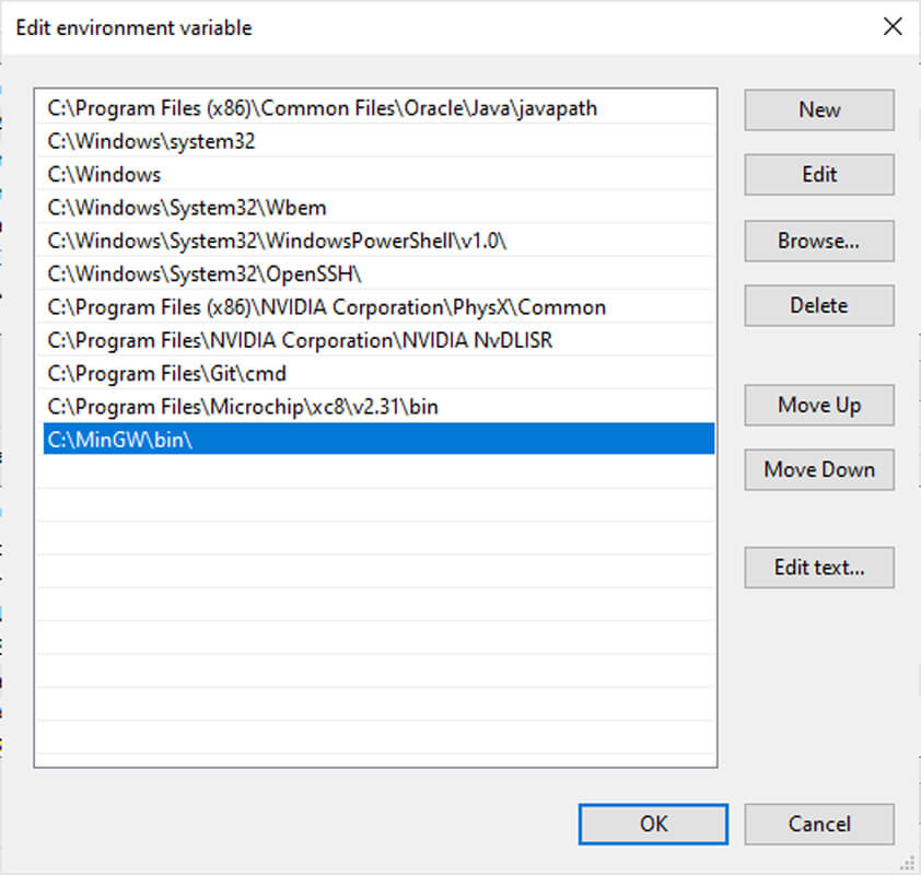
▸ Update PATH
Once everytool is on the computer, we need to update the PATH in the environment settings Control Panel > System > Advanced options > Environment variables > PATH > Edit
From here we can creta a new path and enter the folder location on our computer.
Microchip Studio installation
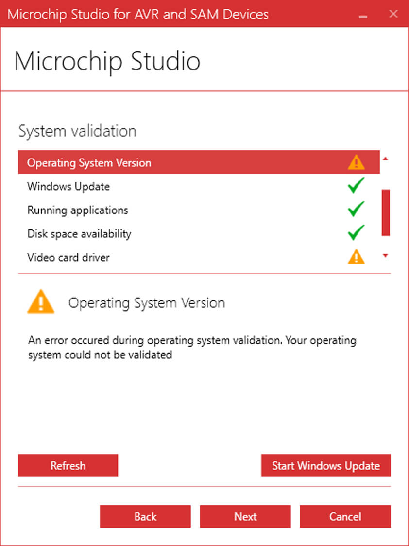
As I was going to use an Atmel Ice Programmer, I chose to install Microchip Studio (the new Atmel Studio).
The installer warned me that I had to be warn about my Operating System Version and my Video Card Driver. So far I had no idea how to resolve this part, and I went forward.
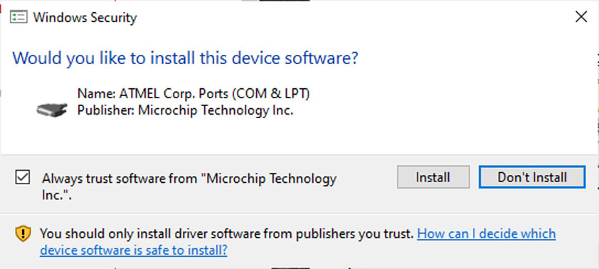
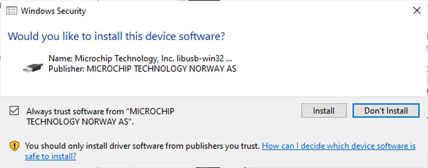
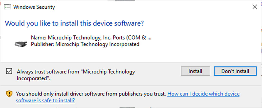
Microchip Studio asked for the permission to install several Drivers.
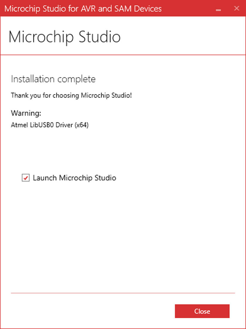
Once installed, the installer warned me again, about the Atmel LibUSB0 Driver (x64), but no information regarding what this warning is about. I went on again.
▸ Check installation
Now that everything is installed, this is time for the sanity check. We are using Git Bash to check if the commands we installed are working :
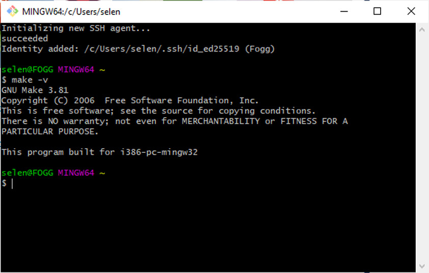
- Check Make GNU version
- Check AVR-GCC version
Type make -v and enter. The version of the software should be appearing under the commande line. If the result is a "command not found" the installation and the Path has to be checked
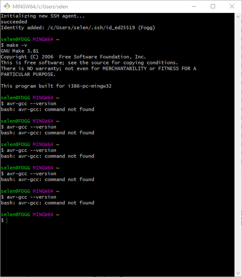
Type avr-gcc --version and enter. The version shouled appear as a result, but I get a "command not found" instead. I checked the installation and the path variables, they are ok.
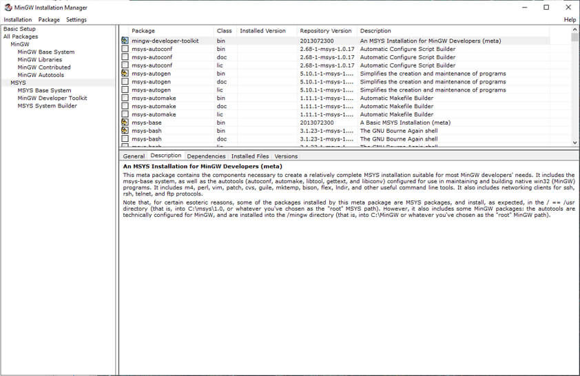
▸ Install MingGW
I tried to find support searching answers on the Worlds Wide Web. I got lost several times into too technical things I could not understand with my actual understandment of what a computer is and how it works and communicates.
I went on several forums where MingGW was installed with Git Bash and I assumed it was the tool missing so that my computer can understand what I am trying to do, I used this tutorial to do so : How to install gcc in Git Bash MingGW
▸ Check again
Once MingGW was installed I run the AVR-GGG version check command again, and nope. I left my computer on this note.
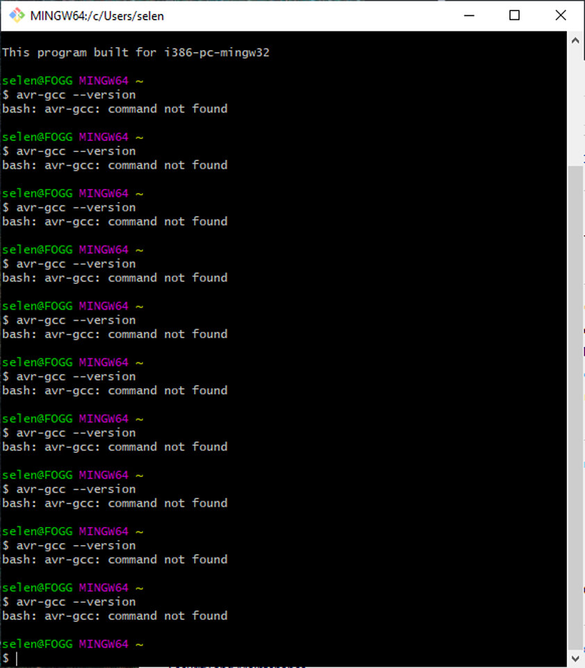
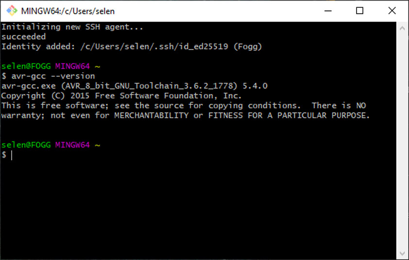
The next morning, I woke up determined to find why it wouldn't work. I ran the command again and it actually worked. So maybe I should have restart my computer after installing all these tools.
As it was resolved I went on with the sanity check :
- Check avrdude
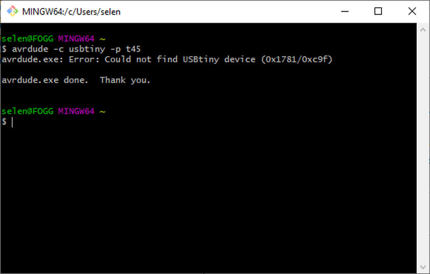
The programmer has to be connected to the computer, then we can type avrdude -c usbtiny -p t45 and enter. The right result to get is a failed initialization, meaning that the programmer is recognized, but the communication failed as no microcontroller is connected to the programmer. I got a "Could not find USBtiny device (0x1781/0x9f)" error.
I did not find a resolution for that issue yet, but I will be looking for it.
▸ Similar issue which seems to have a resolution
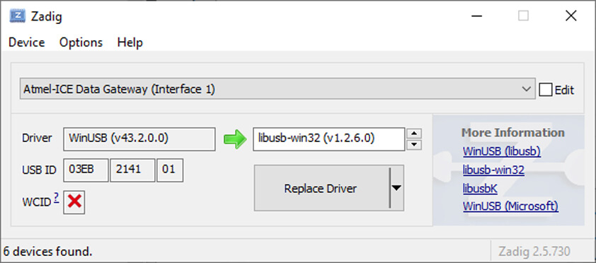
▸ Install the Driver
I downloaded Zadig in order to install the driver for the USBtinySPI, in case it would change something. It didn't.
▸ How it works when it works :
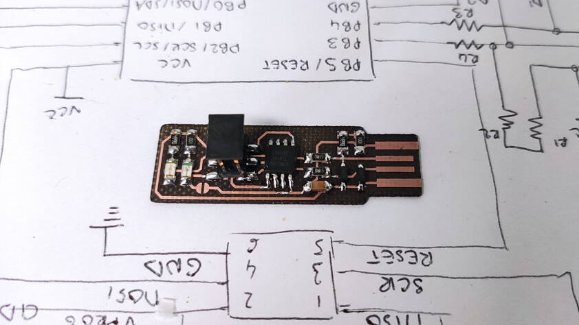
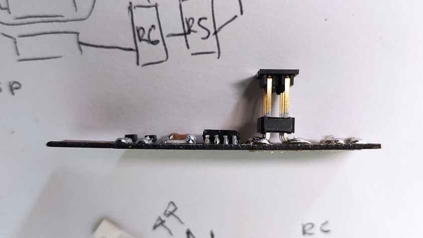
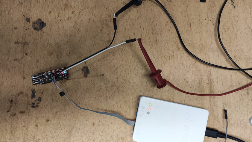
Jonah helped me to go through the FabtinyIsp programmation steps on his computer. Below is a picture of the FabtinyIsp not yet programmed, connected to the programmer to become one.
▸ Building the Firmware
I did not go through this step using Windows. I used Jonah's file during this process. Later I could build the firm using the Ubuntu environment, it is documented at the bottom of this page.
▸ Programming the device
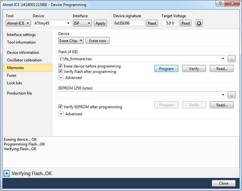
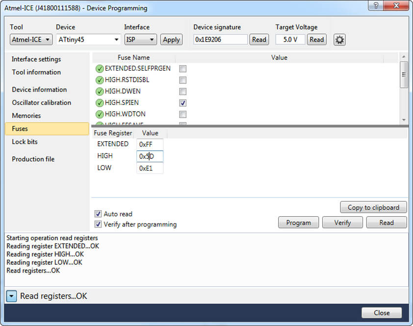
He uses Atmel Studio 7 on Windows 8, the first step is to open this software and to click on the Device Programming icon.
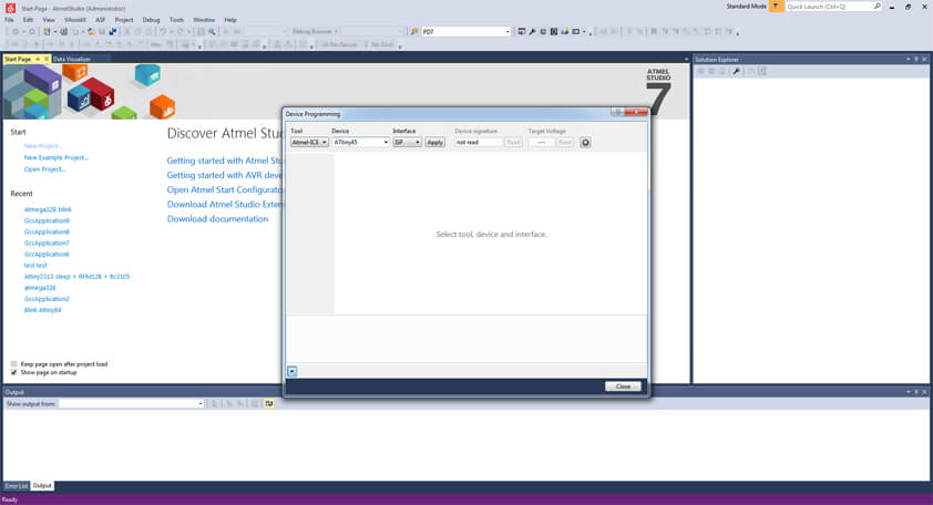
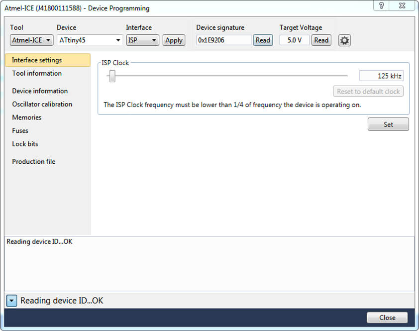
In the Device Programming window we have to specify the programmer we are using : An Atmel-Ice, the device to be programmed : an ATtiny45, and the interface with which it will be programmed. Then, when we click on "read" the microcontroller signature appears "0x1E9206".
We need to go to "Memories" in the left panel, from this menu we can import the firmware HEX file which contains the procedure the microcontroller has to follow. When everything is set up, we can click "Program".
▸ Setting the Fuses
The before-last thing to do in the Device Programming windows is to reach the Fuses menu in the left panel, from there we are going to "set the fuses that control where the microcontroller gets its clock source from" (quoted from the tutorial). This step will allow us to test the USBfunction of the board.
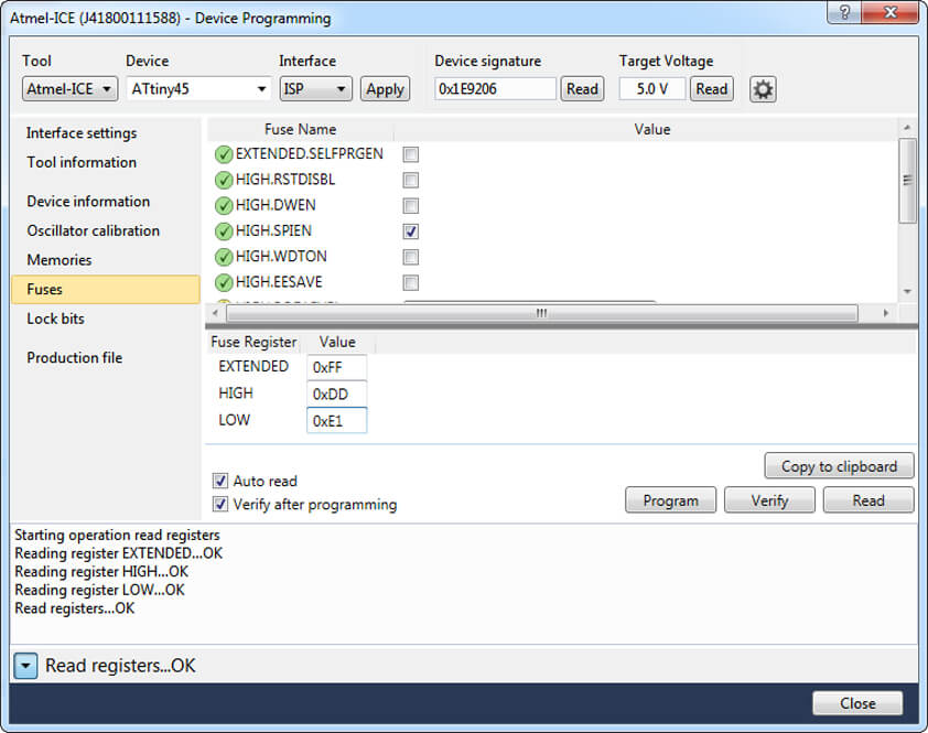
When clicking "Program" in the Fuses menu, a Driver Software Installation appears and the programming process begins.
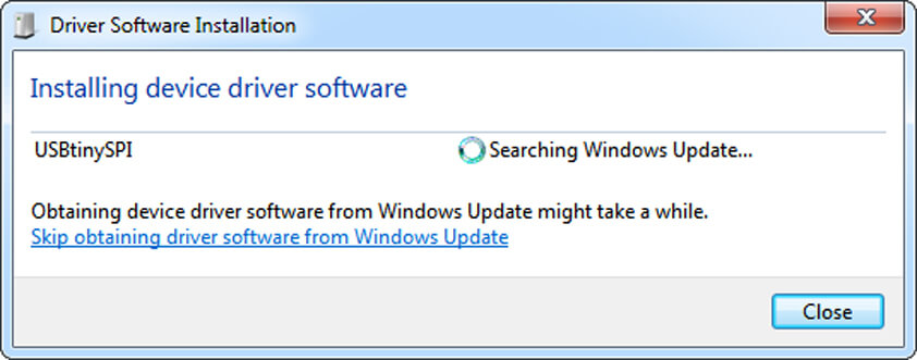
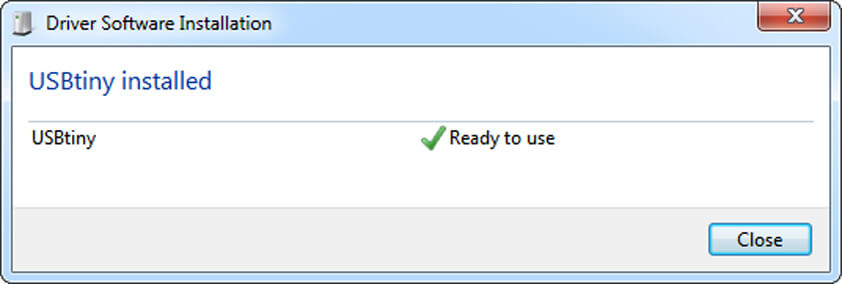
▸ Checking the USB Functionality
Once the board is programmed, and before desoldering the jumper that will restrain us from programming this programmer again, we have to make sure it works. To check this I connected it to several devices :
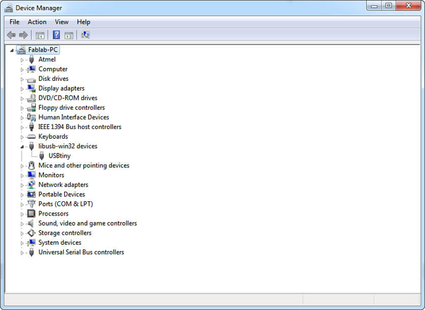
- Jonah's computer, Windows environment : In the Device manager "USBtiny" device appears.
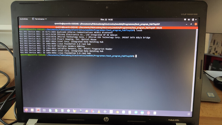
- Quentin's computer, Ubuntu environment : Type the
lsusbcommand, in the result "Multiple Vendors USBtiny" appears - My computer, Windows : I typed the
avrdude -c usbtiny -p m8(it should have been t45 instead of m8), and the "AVR device initialized and ready to accept instructions" appears.
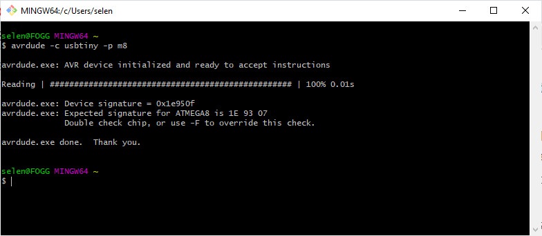
So it seems to be working !
▸ Blowing the Reset Fuse
As the usb function seems to be working perfectly well we can't blow the reset fuse. Once this fuse is set, it will disable this chip's ability to be programmed again, it disables the reset pin of the board so it can be used to program other boards. The value to change is written in the Makefile.
I don't think I am doing it well, it could have been better, cleaner, but I multimeter-checked it and no connection between these pins, and no shorts around. At this point the board finally becomes a programmer.
▸ Using the FabtinyIsp
To make sure this is an efficient programmer we have to make it program something.
▸ Burning a bootloader to an arduino
I followed a tutorial to burn a bootloader on an Arduino, using the FabtinyIsp and the Arduino IDE : Utilisation tutorial for the FabTinyIsp
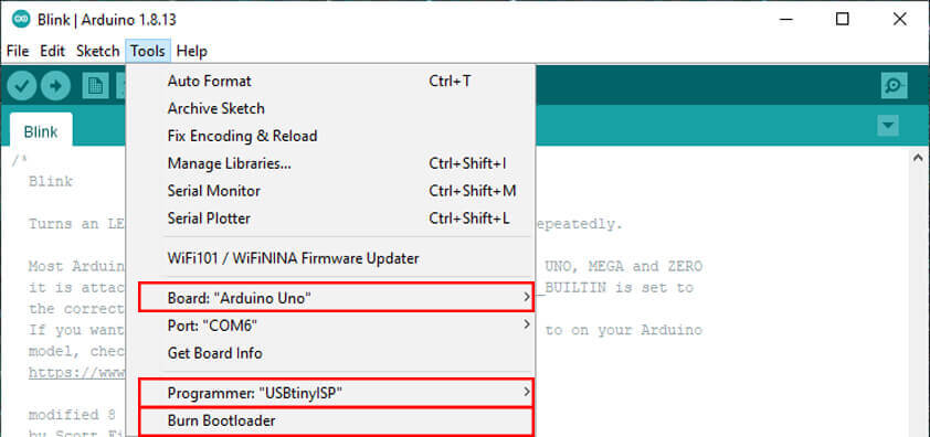
- Connect the ISP in the right orientation on both the programmer and the board to program.
- Open the Arduino IDE
- In the menu select Tools > Board > Arduino Uno (in this case)
- In the menu select Tools > Programmer > USBtinyISP
- Go back into Tools > Burn bootloader
- The next step that should appear is our communication LED blinking as well as those on the Arduino board.
- The burning bootloader is done.
▸ Programming an Arduino using a USBtinyIsp with the Arduino IDE
Then I followed another tutorial to flash a program from my FabtinyIsp : Instructables tutorial
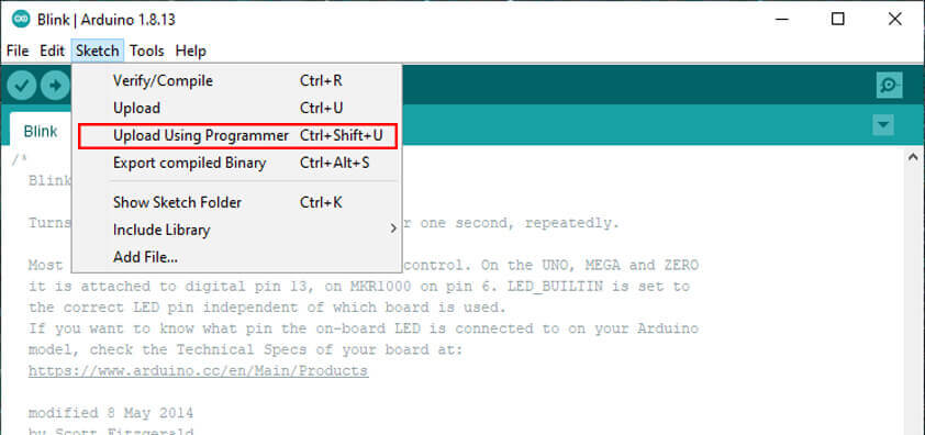
- Connect the ISP in the right orientation on both the programmer and the board to program.
- Open the Arduino IDE
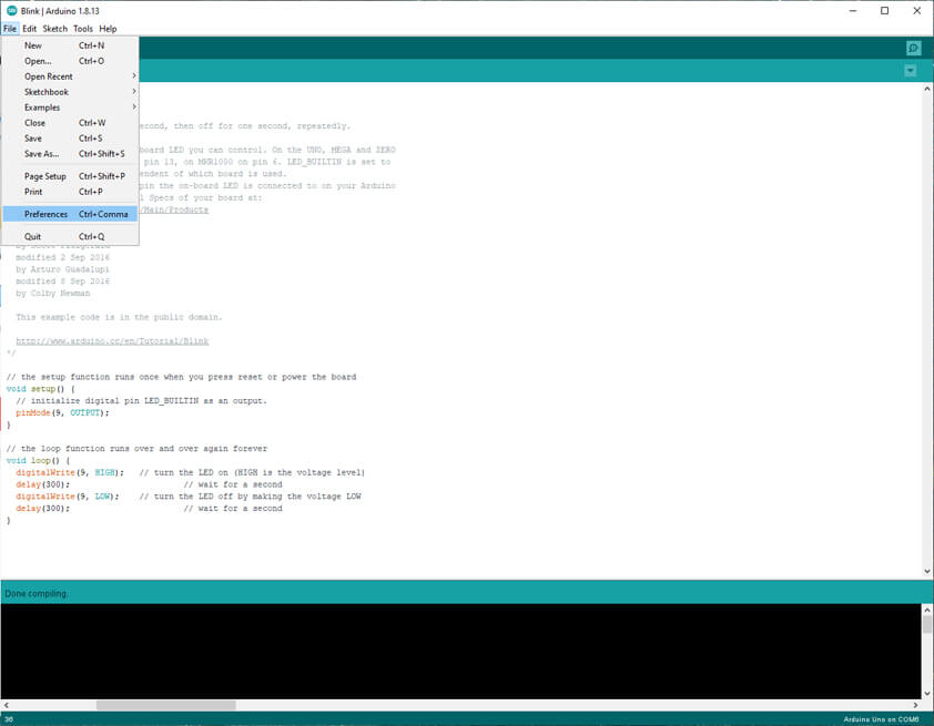
- In the menu select File > Exemples > 01. Basics > Blink - Open the Blink Sketch
- The sketch is using the built-in led to make it blink which is the pin 13, but it is also a pin used by the SCK connection, so we have to change it to another pin, the 9th in this case (So a LED, a resistor, two wire jumpers and a breadboard.).
- Once it is set, go to menu and select Sketch > Upload Using Programmer
- This is the programmation step again and a lot of LEDs are blinking.
- The LED on the breadboard is blinking, yay.
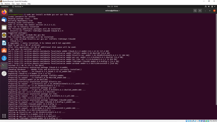
▸ How it works on Ubuntu
I installed Virtualbox on my computer, created a Virtual Machine and then installed Ubuntu in it. From there I could follow the starting tutorial following the Linux Software installation. This was much easier :
- Enter his in the command line and add your password :
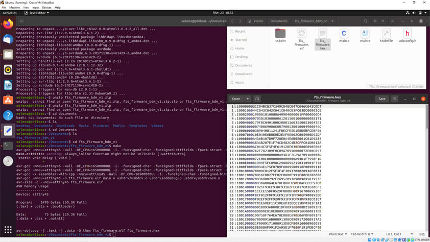
sudo apt install avrdude gcc-avr avr-libc make - Get and build the firmware by downloading it. Unzip it and from the command line run
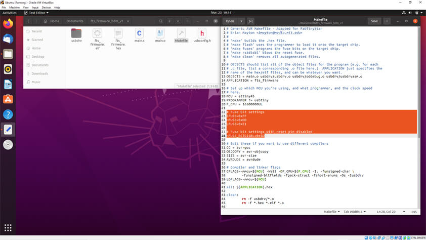
makein the source code directory. If it is correctly completed there is a new file called fts_firmware.hex in the directory. - Program the ATtiny45 : Open the Makefile file and verify/specify the programmer you are using. I chose "usbtiny" As I only have my board, which is now a programmer. I highlighted the fuses values I wrote about earlier in this documentation.
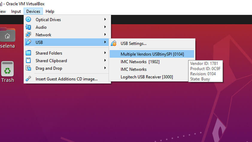
- I connected my board to the usb of my computer using a usb extension cable, but the LED did not turned on. However in the Ubuntu Device menu, the USBtiny appears as an USB device.
▸ How to get an Hex file using the Arduino IDE
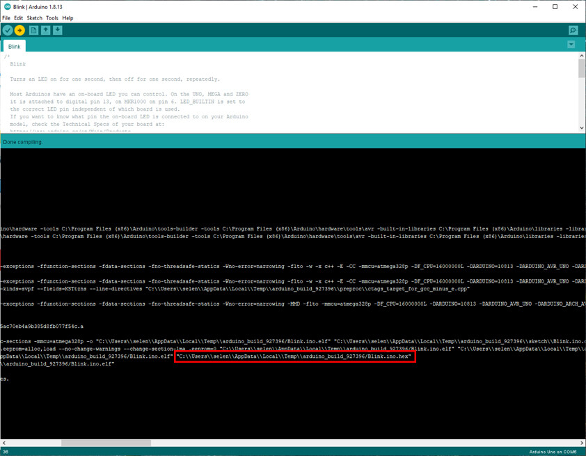
I followed another tutorial to get Hex files from arduino sketches, this will be useful and it is pretty simple. Here is the tutorial, and here are the steps :
- Open your working sketch on arduino
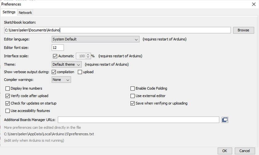
- In the menu select Preference
- It opens a window in which at the line "Show verbose output" you have to tick "compilation"
- In the menu select Sketch > Verify/Compile - During the compilation you can see all the commands Arduino is running - When it is done compiling you can find the adress to the sketch Hex file in your computer.
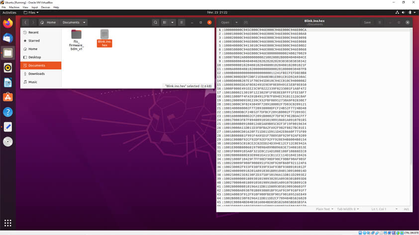
- I copied the hex file in ubuntu and opened it there.
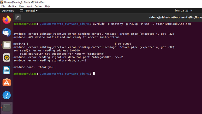
▸ Using the programmer with Ubuntu
I tried to flash a program to an arduino using Ubuntu's Terminal. I first had a issue as avrdude could not find the USBtiny device. This was quickly resolved by clinking on the device in the Ubuntu's Device menu.
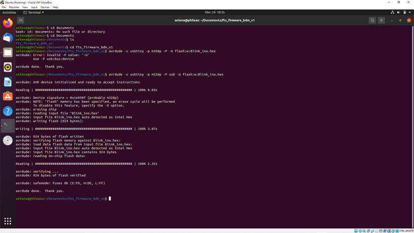
Then I tried to flash the sketch I got the hex file from (a blinking LED which is blinking faster than the previous sketch). To do so I typed the command avrdude -c usbtiny -p m328p -P usb -U flash:w:Blink_ino.hex but it resulted in an error. I can't find why at the moment.
I gave it another try, I changed the file's name which was "Blink.ino.hex" to "Blink_ino.hex", and kept the same command, it worked !
▸ Conclusion of the week
I learned a lot this week, and I everything did not work like the tutorials pretended it did, mainly because of outdated links. But at the moment I have an environment which cannot program a FabtinyIsp into a programmer yet, but which can program other boards using it as a programmer. Then I have a second environment, where I can maybe program a programmer (I still have to make another FabtinyIsp in order to test that part), and with which I can also program another board using the programmer I've made.