The Fourth week of fab academy focused on electronics Production. Our goals for this week were the following:
Make an in-circuit programmer by milling the PCB, program it, then optionally, trying other processes
Document everything!
Described the process of milling, stuffing, de-bugging and programming
Demonstrate correct workflows and identify areas for improvement if required
ISP [in-system programmer] is a chip or a component that allows in-circuit serial programming. Which is the ability to program devices while being installed in a complete system rather than obtaining a pre-programmed chip and installing it to the system.
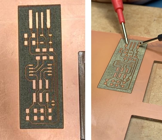
This week’s task was to fabricate and program the FabTinyISP with reference to the tutorial provided.
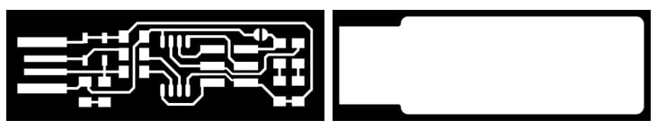
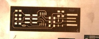
The first step to fabricate this particular ISP is to obtain the traces and the board outlines for the chip from provided in the tutorial.
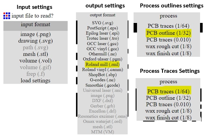
Both pictures shown above have .PNG file extensions, which is not suitable, as the software used for the milling machines only reads files with .rml [Red line markup language file] extension. Therefore, the files need to converted to the correct type using an online tool called FAB modules. The file conversion is performed as following:
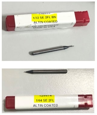
PCB Traces (1/64) – refers to the traces milling bit size.
PCB Outline (1/32) – refers to the outline milling bit size.
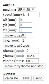
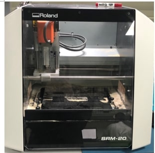
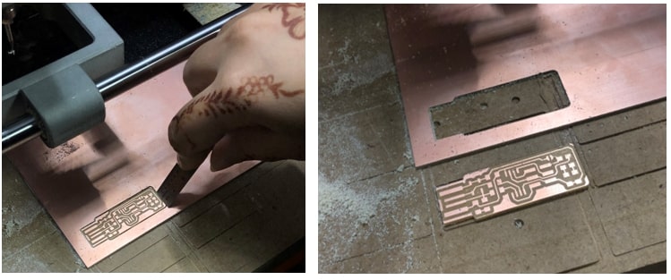
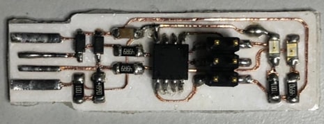
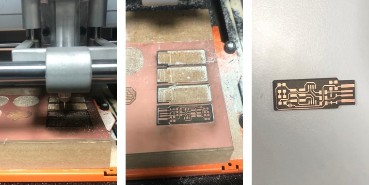
To fabricate the ISP chip, we are using a Roland SRM 20 machine to engrave the traces and the outlines on an FR1 [copper clad Flame Retardant 1] printed circuit board. We are using the FR1 boards instead of the commercially found FR4 due to their safer nature, as inhaling the milling dust of an FR4 fiberglass material may lead to serious health hazards.
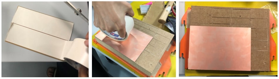
First, we mounted the FR1 plate on a medium density fiberboard (MDF) to secure the plate while milling as well to keep it levelled. The plate is adhered to the MDF using strong double sided tape where the plate is then pressed to adhere and level up properly.
The following steps describe the process of calibrating the machine for the milling.
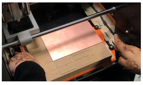
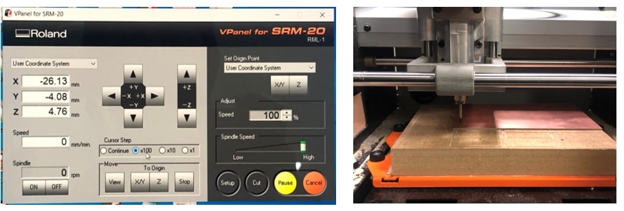
Before going and choosing the pattern to be engraved, we can perform an experimental engrave to ensure that the milling bit tip is close enough to the surface to engrave properly. This is done by pressing the ON button under spindle on the software page. The milling machine launches, and if the Z axis was calibrated correctly we can observe the machine engraving an indentation on the origin point and dust starting to gather.
Once the experimental engrave is done, we can then click on the cut button which opens another window. Then the existing operations should be deleted and we should add our traces pattern file in .rml and finally click on output to launch the machine. The milling bit is then changed again following the previous steps of setting up the machine and the steps in the software are repeated to engrave the outlines.
Important point: The inner pattern [traces] should always be engraved before the outer pattern [outlines]. As engraving the outer pattern first releases the chip or the piece from its place, making it difficult to engrave the inner patterns without overly moving.
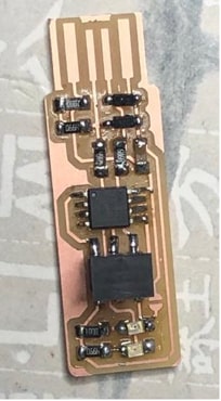
Ahead of welding, we should prepare our stations and components used. I made sure that everything was close by in my station having good source of light and good ventilation for the welding fumes.
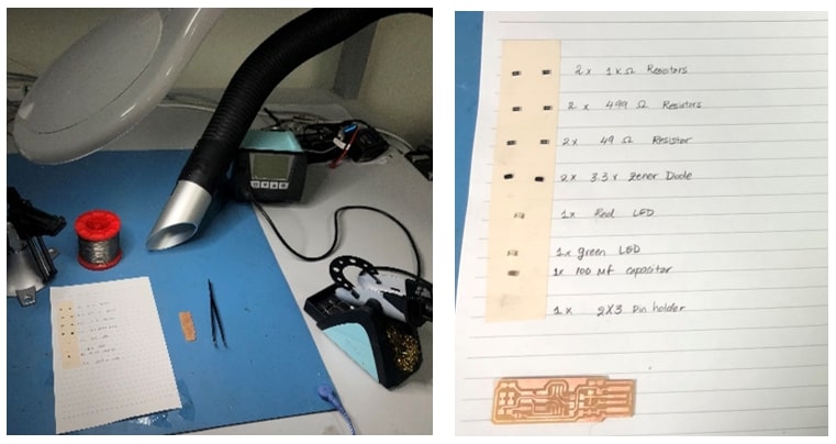
The components I used are listed below:
| Quantity | Component |
|---|---|
| 1 | Atiny 45 8 bit microcontroller. |
| 2 | 1k Ohm Resistors. |
| 2 | 499 Ohm Resistors. |
| 2 | 49 Ohm Resistors. |
| 2 | 3.3 Volts Zener Diodes. |
| 1 | Green LED. |
| 1 | Red LED. |
| 1 | 100 nano-Farads Capacitor. |
| 1 | 2X3 Pin Holder. |
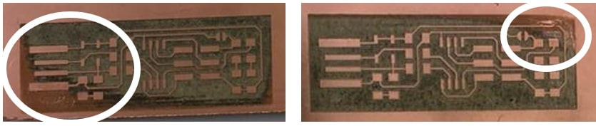
I started soldering the components on paying attention to the orientation of some components. For example, the LEDs have a slight green line on one end indicating the side connecting to ground. The Zener diodes also have in indication to the ground which is a fade sliver line on one end [which can be a tad difficult to see if not under a direct source of light]. The Atiny 45 microcontroller chip has a dot that indicates the first pin and the orientation of the chip.
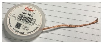
while soldering, I came across times where I would apply too much solder melt on a component, thus I used the de-soldering wire to remove the extra melt and prevent any damage or short circuit.
And finally I checked with a multimeter for any shorts between VCC and ground points, and fortunately it yielded a success! (phew!)
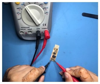
Note: Remove the extra layer of copper on the tip of the “USB” as it may cause a short circuit.
Since the platform I’m working on is Windows 10, it means that I need to setup my development environment to be able to build the program into the board. I have used the tutorial as a guide to install the toolchain into my windows system.
The programs that I have installed are the following:
I have downloaded each file/software tool and unzipped/placed them as instructed. Then I added the paths of GNU toolchain, GNU make and AVRdude by going to the control panel >> system and security >> system >> advanced system settings >> environment variable >> double click on paths >> and add the new paths.
(or to make life simple, just search for environment variables in the search bar and follow up from there!)
Important note: Copy the file path of your own saved files instead of the paths provided in the tutorial as sometimes the paths can be outdated, or the files can have different titles.
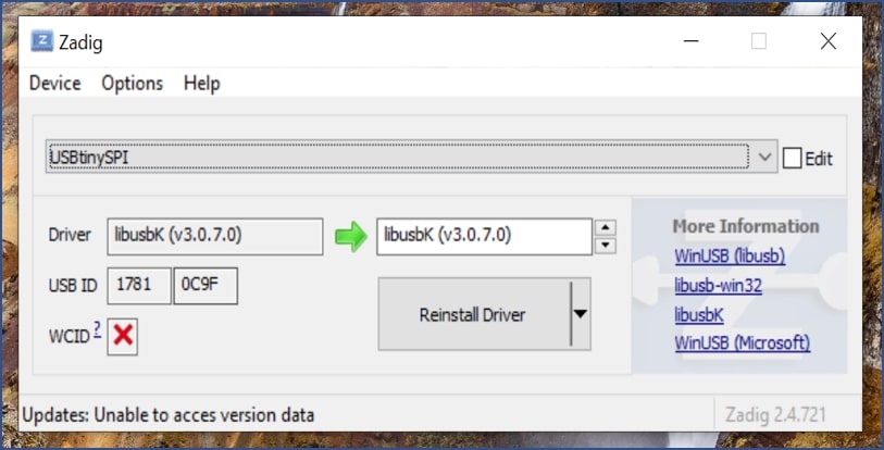
Next, I have launched Zadig, checked for my device and re-installed the driver.
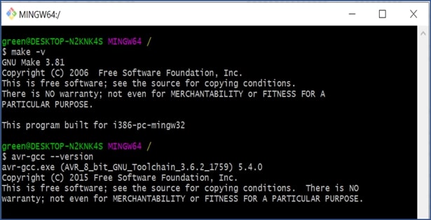
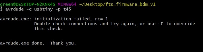
Then I had to check whether the programs were installed correctly. That is done by accessing git bash tool and typing make -v to check for the GNU make software, avr-gcc --version to check for the GNU toolchain, and avrdude -c usbtiny -p t45 to check for AVRdude software. However in my case, running the AVRdude command doesn’t show or do anything, this issue will later be discussed in the “problems faced” section.
Next, I opened the firmware directory in gitbash and ran run make to create a .hex file.
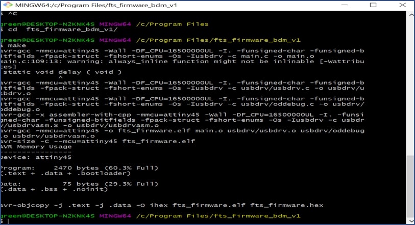
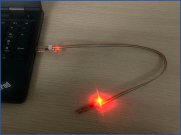
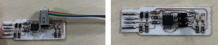
Once the hex file was created, I carefully plugged in my USB connector and the ISP board provided by Hashim connected along a ribbon to my own ISP board and observed as the red light on both boards went on with no problems.
To create the ribbon cable, I used a 6 color wire cable, and two 2x3 connectors. I inserted each end of the cable into a connector head, and hammered the head to secure the wires, making sure that the color order are identical at each end.
The main point of connecting the two ISPs via the ribbon is that the VCC and the GND points should be connected the same along the two ends of the ribbon as shown below:
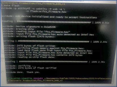
Then I ran the commands make flash in gitbash. The command erases the target chip (my board) and programs its flash memory with the contents of the .hex file created previously.
Unfortunately, hence this step requires Avrdude to be completed, the process was forced off due to Avrdude not working on my laptop. Thus, I have used Hashim’s Laptop to perform this step along with the following few steps.
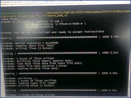
Next, I ran the command make fuses which sets all the fuses except the one that disables the reset pin.
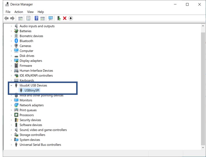
To check the USB functionality, I had to plug in my own board directly and check if my computer detects the device. That is done by accessing the device manager and checking under libusbK USB devices.
The last step of programming the ISP is to blow the reset fuse by running make rstdisbl. This command will disable the ability to re-program the board in the future by changing the reset pin of the board to a general purpose input output pin.
To check that the ISP board is working properly as a programmer, I had a friend use it to perform the commands above to program hers and thankfully it worked properly!
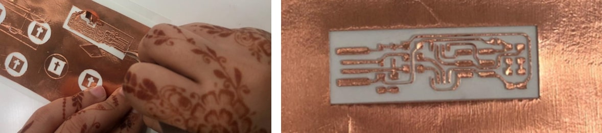
As an extra step, we decided to try producing a flexible ISP using the Vinyl cutter and copper sheets. Honestly, when I saw the documentations of previous students in fab academy, I thought that producing a flexible ISP would be much easier, and less time consuming than using the milling machine.
Well, I was wrong. We spent a good amount of time trying to find out the best cutting settings that would produce a sustainable chip. Everyone pitched in with ideas for our trials and errors and the process turned into a group work which can be found in our Group Assignment page.
| A summery of the production process that worked best for us: |
|---|
Piece so the vinyl cutter can take the dimensions of the sheet.140 % ~ 150 %.cutting icon on the top tool bar.The process of weeding and soldering the components were done individually, thus is documented in details below.
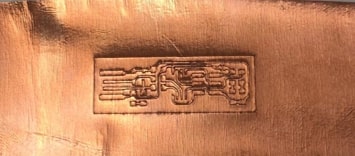
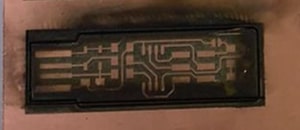
This is the chip I produced for using the vinyl machine. It is noticed that it’s looks much better than its decedents, as the traces and pads are clear and wide enough for soldering.
The next step was the weeding, where I carefully pulled the excess copper around the pads and the traces. A useful tip is to use a good pier of tweezers to remove the large parts, x-acto knife to release any parts that might get stuck, and some small scissors to cut large pieces as you weed away the copper.
Next, I applied some double-sided tape to the back of the tracing paper and adhered it to a piece of acrylic I’ve cut previously using the milling machine. And finally removed the excess tape and excess copper on the sides.
Next was the soldering. Now this step was a bit more difficult to compared to the chip produced using the milling machine.
When soldering, the traces or the pads (sometimes both!) would lift off the tracing paper, the soldering bits would not stick to the copper so I was extra careful and patient in soldering the components. Also, settings the temperature of the soldering iron too high caused the tracing paper underneath to melt so I kept the temperature at 350 which was ideal for my soldering.
Then it was the time for programming. I used the previously mentioned steps to program my ISP. However, when I tried plugging the ribbon off, the traces came out with it :( and I had to apply some solder on it to fix it again!
This step (like many others!) was full of successes, failures, frustrations and proud satisfaction.
We tested our Trotec fiber laser machine to characterize it’s cutting settings before producing our own chips. All the details for the process along with the results are documented in the Group Assignment page.
To produce my own chip, I worked with my fellow student and friend Fatima to test the settings on for the ISP chip. We have used this page as a reference.
For our first trial, we replaced the C02 lens in our trotec machine with the fiber laser lens.
Then we uploaded the traces on CoralDraw keeping the color as it is (black) for the purpose of engraving, and clicked on print. The detailed process of using the Trotec laser machine can be found in Week 4 page.
Attempt 1: The start
The settings that we used for this test are the following:
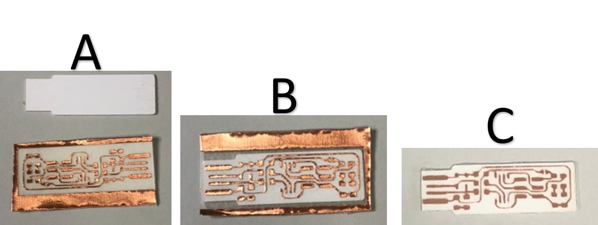
And the result was this:
The traces and the pads of the PCB were clearly visible and well marked. However, a good amount of copper remained on the surface of chip causing short circuits to almost every single connection when tested using the multi-meter. Verdict: Absolute fail.
Attempt 2: The success!
For the second attempt, we kept all the settings used previously, and increased the passes to 10 as it proved a good result in our group assignment test.
And the results?
They were amazing! Traces and pads fully outlined perfectly, not a single short circuit when tested using the Multimeter. Verdict: SUCCESS!!!!.
Attempts 3 + 4: The disappointment !
Hence the previous settings worked perfectly for us, we decided to engrave another board (since we worked together to produce the chip). And well, this is how I felt.

We engraved the boards using the EXACT SAME SETTINGS, but we missed the fact that the FR1 plate was not levelled properly on the MDF board, thus resulting in improper removal of the copper and short circuits. Verdict: Disappointing fail
Attempt 5: The cut trial
The FR1 plate had to be changed, since there wasn’t enough space for another engrave. But before that we decided to try cutting our successful PCB attempt.
We changed the lens back to the CO2 lens., and we’ve used the cutting settings provided in the tutorial. And it almost worked.
The outlines were very charred, and only one side of the outlines was properly cut hence the reference point was lost.
A TIP : Try not to move the placement of the engraving job on the software, or else the outlines would be offset-ed and you’ll have to manually guess the reference point .. which proved to be a bad idea.
Verdict: fail.
Attempt 6: Another trial
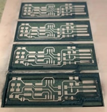
We came back to the Trotec machine after a very much needed break. And decided to engrave a several ISP chips again. We used the successful engrave settings and it yielded perfect results! The process of took about 1 hour and 27 minutes.
Then we replaced the fiber lens with the CO2 lens (again) to attempt the cutting again. And used the previous cut settings. The outlines were not cut! We tried different settings, varying the power, speed and the passes every time but the outlines just wont cut!!
So after thoroughly looking at the causes of the error, we found out that the lens was not installed properly, thus the focus was wrong. After fixing the lens and trying again, several times, it still didn’t cut the traces.

This is what it looked like after all the trials:
We decided that by this point, we had two options. Either we can take the risk of cutting the outlines using the milling machine, trying to use our luck to manually locate the reference point and cut it. Or, we could use a saw to cut the outlines.
So I went with the easier one (in my opinion!), the milling machine option. I tried to locate the reference point by eye and I started cutting. The results were considered pretty good.
Because what’s life without a set of challenges!
Some of the software required installation in windows had outdated links in the tutorial guide which lead us to manually search for the software and choose the version that best suited our computer systems (links for the updated programs are mentioned above under programming.)
Much like the outdated installation links, the paths in the tutorial were outdated and referred to older versions of the software. Thus copying the exact path from the tutorial rendered a fail in the system recognizing the software. The solution to this is to copy the file path directly of the downloaded software files.
The solder jumper! Something that I completely missed on while soldering my components! When I plugged on my ISP chip to the ribbon and the programming ISP borrowed from Hashim, I noticed that the red light was not turning on and the commands I ran rendered no results! Soon I discovered that the jumper solder was not even soldered! thus not completing the circuit and not providing power to the rest of the components. The only solution to this was to go back and solder the part, so I did just that!
One of the main tools required to set up my ISP was not working as it should be. After re-installing the files, and checking the paths for any errors, I tried running the command to recognize the tool on Gitbash, but the results shown were nothing, not confirmation of the existence of the tool nor an error message.
Assuming that I can skip this step, I moved forward to the next few commands and was stopped again by an error message when I tried running the make flash command which required the usage of Avrdude tool.
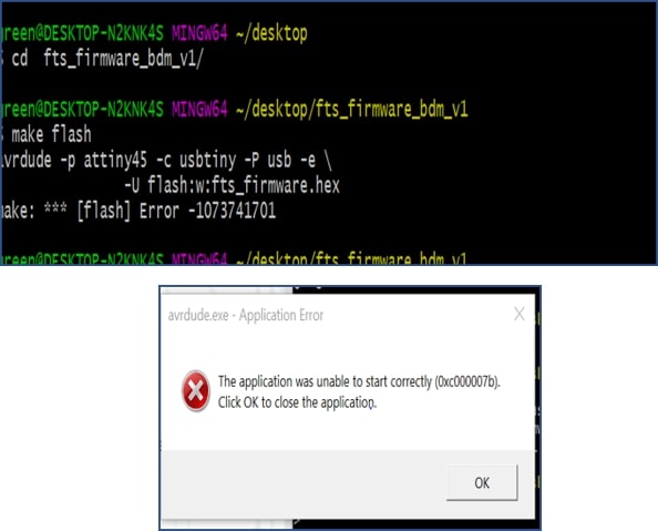
The problem is apparently exists for all my colleagues with a windows 10 x64 bit systems installed. The problem main cause and solution is yet to be known.
I tried re-installing the AVR Gnu tool-chain using Hala’s wonderful and very useful documentation to solve my AVR-dude problem.
The steps that I followed:
Install WinAVR 20100110 and launch it.
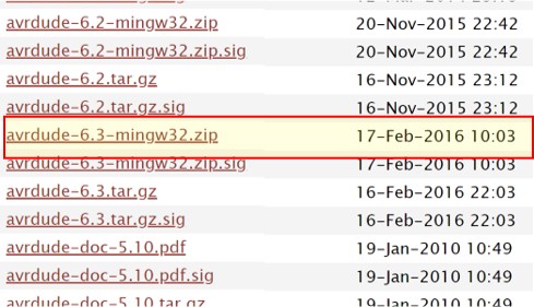
Open the WinAVR folder and find the folder bin. Then delete or move these two files elsewhere: avrdude.conf and avrdude.
Replace the deleted folders with the newer version of them Version 6.3 2016.
In control panel > systems > advanced system settings > environmental variables > path > edit > delete the old AVR (if installed) path and add the new path (../WinAvr/bin).
Connect the ISP programmer to the laptop, and launch Zadig, select the programming > select “libsub-win32 (v1.2.6.0)” > replace driver.
Open the fts_firmware_bdm_v1 folder and open GitBash.
Make sure that all the driver are installed properly:
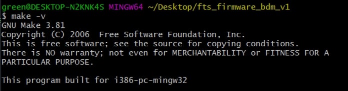
Make -v
Avr-gcc –version
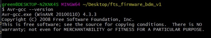
avrdude -c usbtiny -p t45
This time the AVRdude was installed properly as shown.
make flash
make fuses
make rstdisbl
