In this week we were required to design a circuit board using a software called eagle. Personally speaking this is my second time using this software, my first was during the winter camp but to be honest I didn’t get familiar with it back then and I felt that I had to use this software more if I wanted to truly know the ins and outs. So this week I faced some issues while trying to design the circuit board but I want to give some credits to my colleagues Maha and Fatima since they helped me a lot and they ensured that if I had any concern they’ll help me with it, and thankfully I was able to finish the circuit board on time. I was under stress since we were a few days away from the deadline and I was a bit late, but in the end I was able to finish it on time and during the submission date I performed the milling operation on the circuit board and then I soldered it. All of this has been done in a good time and it really teaches me a lesson and that is to always finish my work on time and never postpone any work just before the deadline by a couple of days
The link of the group assignment can be found here
Now I’m going to explain the steps that I did to design the Attiny 44
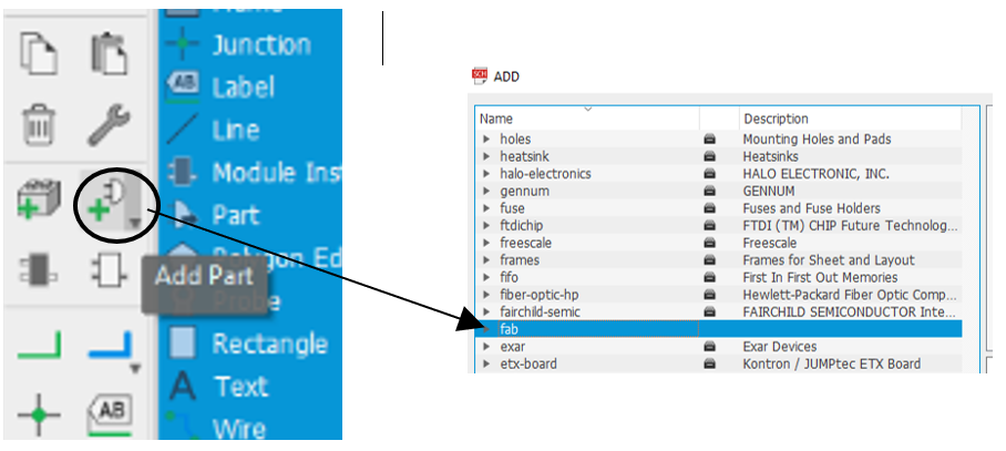
Step 1: I opened eagle software and saved the file under a specific name then I opened the schematic page and chose add port:
Step 2: I added all the components that I required to design the circuit board from the fab library. This option was already included within the software. Below are the name of the files. Since we were required to add at least one input and one output to our circuit, I decided to add an LED along with a button. The components I used are listed below:
Attiny 44
ISP Header
10K ohm Resistor
499 ohm Resistor
20 MHz Resonator
FTDI Connector
1 uF Capacitor
Push Button
LED
(source volatge - forward voltage)/(forward current) to determine the value of resistor needed,
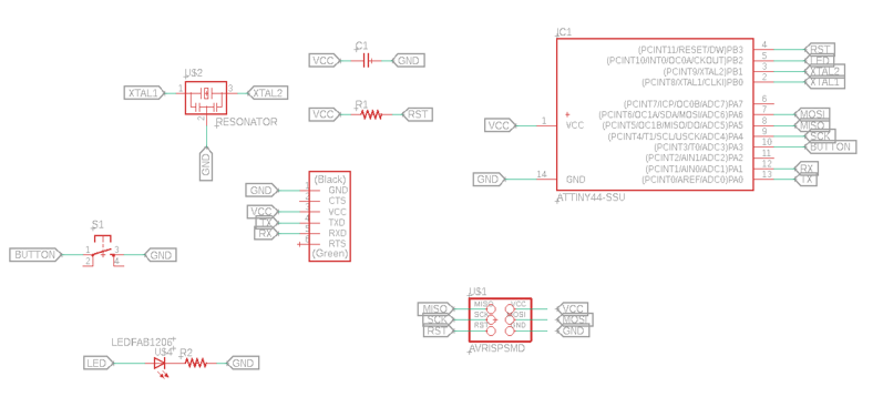
(5-2.5)/0.02 which would equal 125 Ohms. That is the minimal resistor value that can be used for the LED. But what’s available in our lab is the 499 ohm resistor as a minimum value of the resistor in the lab so I used it.Step 3: I placed the components just as our instructor Hashim taught us with the connector having its VCC side on the right and the GND on the Left and used tags to connect the components together instead of using direct links, hence it would be easier to modify later, and much more comfortable on the eye.
Step 4: I then changed the page that I was on from schematic to board page using the switch/generate board tool on the top tool bar.
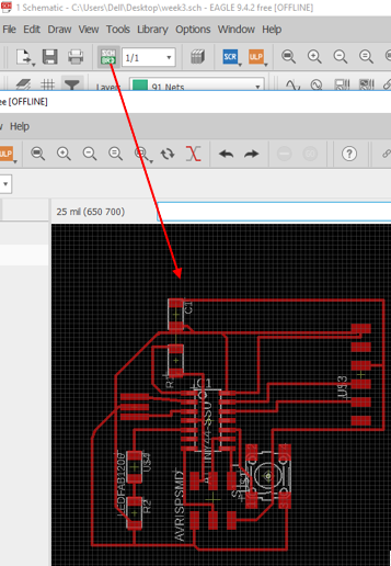
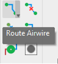
Step 5: I used the airwire tool to do the connection again and arrange the components in a way to ensure that there will be no intersection between any two lines
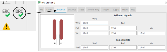
Step 6: I clicked on DRC and changed all the clearance values to 17 because the mill bit for the milling the traces is (1\64) which is equal to 0.0157 to be exact.
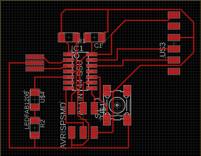
Step 7: This is the final shape of the circuit board.
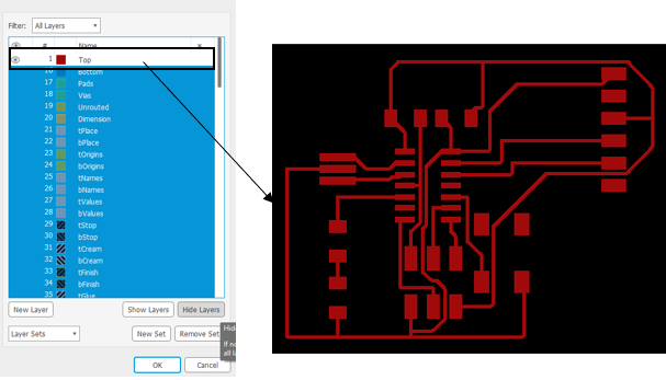
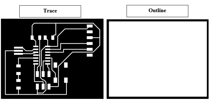
Step 8: I clicked on layer settings and then clicked on hide for all the layers except the top layer
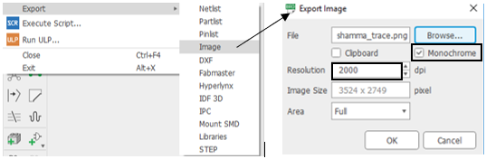
Step 9: Then I had to save the picture so I followed the steps that are shown in the screenshots below.
Step 10: For the outline I used paint software to make the outline and this is result of the outline and trace
Step 11: I opened fabmodulus software and followed the steps that were mentioned during the electronic production week then I had to save them on a flash in order to use them on the computer that is connected to the milling machine.
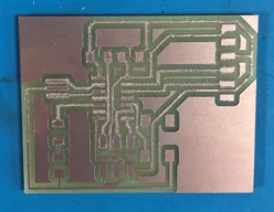
Step 12: Then I had to print the circuit board, So I repeated the steps that I did during the electronic production and this is how the circuit board looks after executing the milling operation
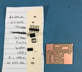
Step 13: I brought the components that I required to perform the soldering operation and I stuck them together on a paper so that I don’t lose them and I’ll be able to find them easily when required and I wrote the name of each component on the paper.
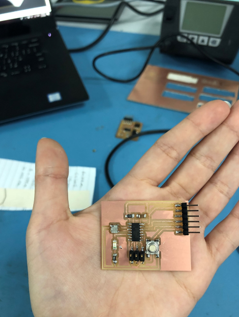
Step 14: This is how the circuit board looks like after the soldering process
My files: