Electronic Design

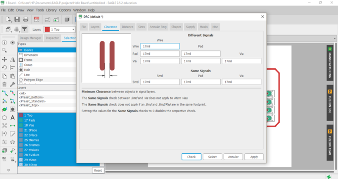
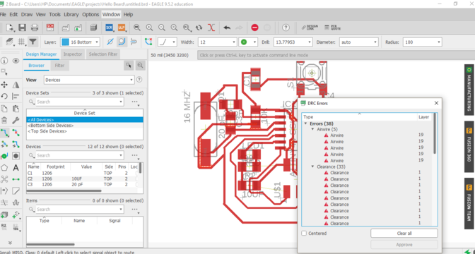
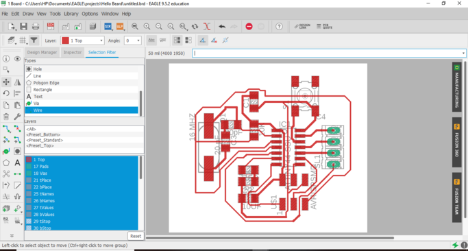
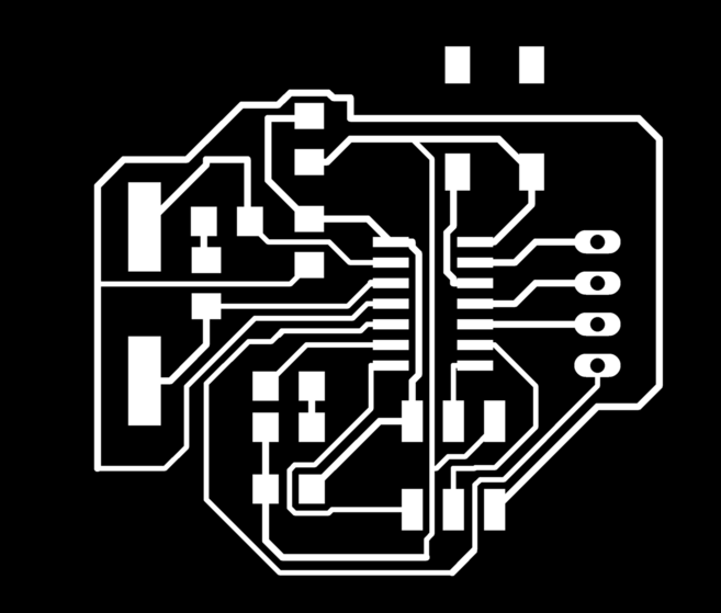
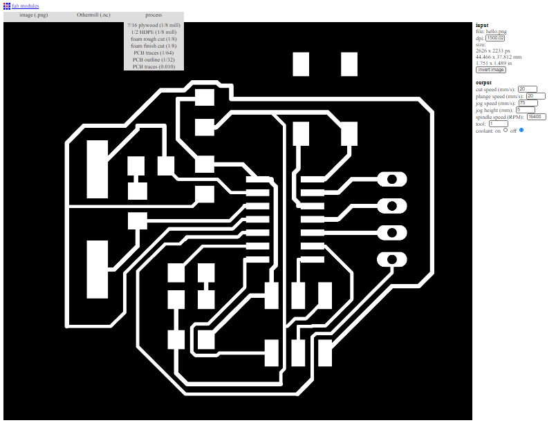
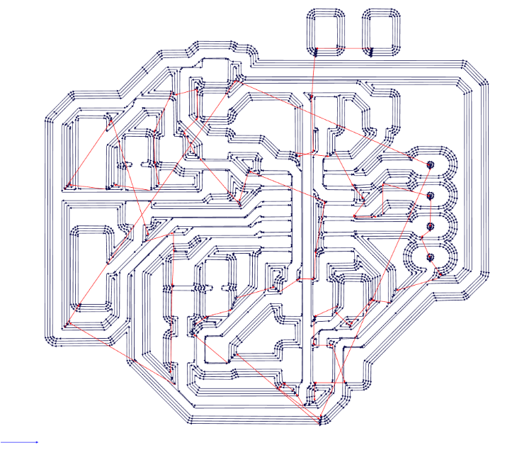
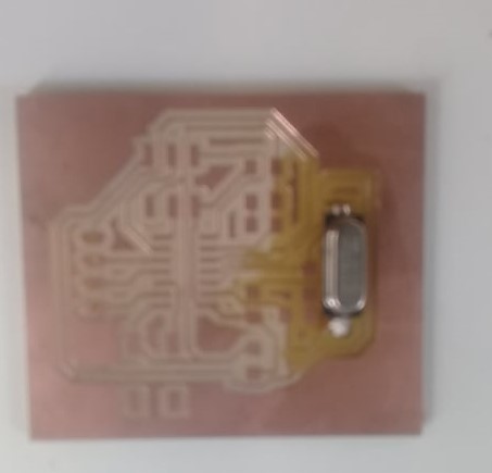
This Week's Objective


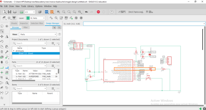
Design, Make & test a PCB

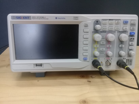
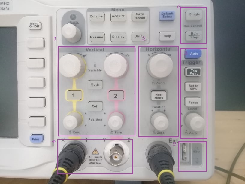
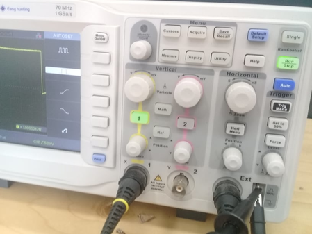
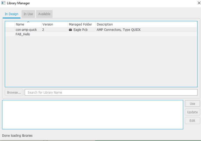
Tools Used in This Assignment
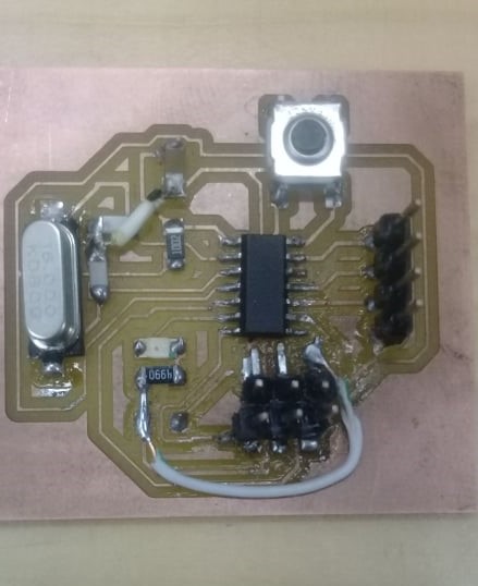
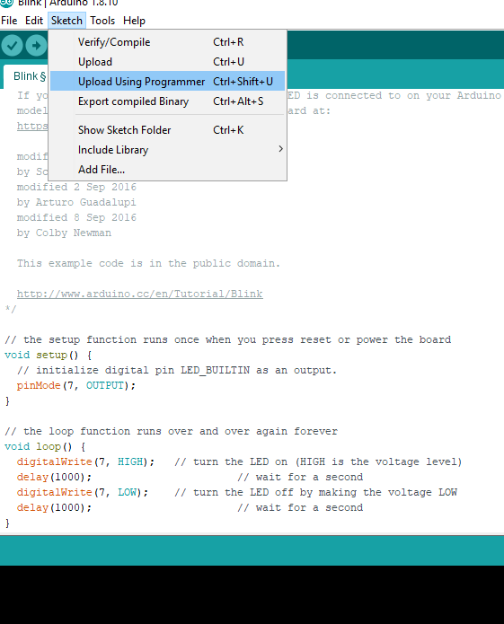


Group assignment

Link for the group assugnment

For the group project this week, we used the test equipment in our lab to observe the operation of a microcontroller circuit board. The oscilloscope we used for this group assignment is Siglent's SDS1072CML+.


I’ll explain how to use an oscilloscope:
  • 1.Vertical Control:Position, Show & Hide, Scale (per division)
  • 2.Horizontal Control:Position, Scale (per division)
  • 3.Trigger:Decide the threshold to catch and capture voltage waveforms and its location.
  • 4.Channels:Inserting probes into it, you can measure and show several waveforms at the same time.
  • 5.Probe configuration
  • 6. Run/Stop and Signal: When Run/Stop is on, oscilloscope continues to record signals to its memory. It is used when you’d like to measure the steady voltage or current.When Signal is on, oscilloscope capture signals at certain threshold you set at Trigger function. It’s like camera.
  • Once the machine is turned on, you can calibrate the machine automatically by first pressing the "Default" button to restore all the settings to its default configuration. Then, plug in a probe into a channel BNC connector on the front panel of the oscilloscope and attach the alligator clips to the Ground Terminal. Finally, click the "Auto Setup" button in the top right corner. In addition, make sure the switch on the probe is also set to 10X.


    We decided to measure the operation of the onboard LED on an Arduino running a simple Blink code. The setting of one of the board's pins to HIGH was accompanied with the onboard LED being set to HIGH. We probed the pin being set to HIGH but if we really wanted to, we could have probed the onboard LED directly.


    Individual assignment

    Designing The PCB


    In this assignment I followed the tutorials to design a pcb. It's again the first time for me to design an electric circuit.I will use EAGLE for this , it's a scriptable electronic design automation (EDA) application with schematic capture, printed circuit board (PCB) layout, auto-router and computer-aided manufacturing (CAM) features.
    So first thing is to import all the required componants. For that a library must be installed first. It's called FAB_hello. It's pretty easy to do that you just have to manage library and add the required files.


    Once I got all the required componants in front of me I started connecting each part to its counter parts. I used labels to assign names to some ports and the program can understand if two componants must be connected by these labels. The other command I used is to assign the values and its just for my referance.

    As shown in the fugure ,I want to add a led and a button . So I started by identifying the pins that are available, for a led I need a digital pin since a led is either closed (no electric current) or open (there is current) also for a button (it is open or closed), the available pins are 5, 6, 10, 11, 12, and 13.


    If I plug the LED directly on the board, she won't like the 5V supplied. With this very high voltage, the current will also most likely be too high.As a result, the LED will heat up and may burn out if you leave it on for too long.that's why I added Aresistor 499 Ohm. Iwill conect them both to the pin number 6 and GND.

    Then I add the button by connecting it to pin number 12 and GND


    There are many ways to draw a schematics, possibly one for each designer, and I figured out that no one is better than another as long as it is clearly readable and concise. It's important to mention thant after creating and editing a schematic it is possible to confirm whether it is electrically correct ,by running an ERC .


    Once it's ready,I took the design schematic to board view and it gaves me the design with all the componants.you will enjoy moving componants and triing to find the good positions.
    The good thing is that board view showes lines that need to be connected. After connecting all the lines with width : 16. I change some setting in the clearance of the DRC


    Then I started correcting errors and wornnings with width wire: 12


    YOU CAN FIND HERE the file ( file.sch andfile.brd )
    Once the board was finished I export a PNG file through the File -> Exoport -> Image command menu, ensuring that the resulting image would be rendered monochrome and with a resolution of 1000 DPI.and I used gimp software to make a cut out for the board


    I used Fabmodules online atFabModules to upload the .png images successively and to generate the G-code for the CNC mill to mill the traces and to mill the outline shape of the PCB


    After that I was ready to mill my board so using the same steps in the electronic production assignment I was capable to mill it and I start soldring it


    after the soldering, I went to the connection test and to correct the unresolved discontinuities with the solder for the removed traces, I had to make jompers with two cables.


    Moving now to the programming phase,first I upload the code of "arduinoisp " on my arduino , the code is under file --> Exemples --> 11.ArduinoISP


    Then I had disconnect the arduino from my laptop and connect it to the Hello Board as showing bellow ( in my case just swap the MOSI and MISO pins in the arduino) , noting that the purple cable wasn't good so i changed it to the brown cable.


    To program mu board there os some changes that I must do on the arduino software. Fisrt thing is that I had to open this link and then copie it in the arduino preferences as showing bellow


    Now l'm able to select my microcontroller which is ATtiny , in Tools I celected (boards: attiny24/44/84, processor : ATtiny84 ,clock :external 16 Mhz and also the port to which the arduino is connected .DO NOT FORGET ABOUT THE PROGRAMMER you schould put it : arduinoAsISP
    THEN I go to the pereferences and check this two boxes


    THEN I click the button Burn the bootloader under Tools to check if my board is OK and it's GOOD


    THEN I go to exemple , choose the blink exemple under Basic and change the "LED_BUILTIN" to 7 beaucause in my schematic I connect my led to the physical pin number 6 which is A7 ( look at the attiny84 pinout page


    void setup() {
      // initialize digital pin LED_BUILTIN as an output.
      pinMode(7, OUTPUT);
    }
    
    // the loop function runs over and over again forever
    void loop() {
      digitalWrite(7, HIGH);   // turn the LED on (HIGH is the voltage level)
      delay(1000);                       // wait for a second
      digitalWrite(7, LOW);    // turn the LED off by making the voltage LOW
      delay(1000);                       // wait for a second
    }


    Then just go to scketch and upload the code using programmer


    And this is the final result YEEEES