7. Electronics design
Group assignment
Individual assignment
It is my first time designing my own circuit,so I have started by downloading Eagle software from Autodesk and read this tutorial to get familiar with the program and know how it works and how to use it.
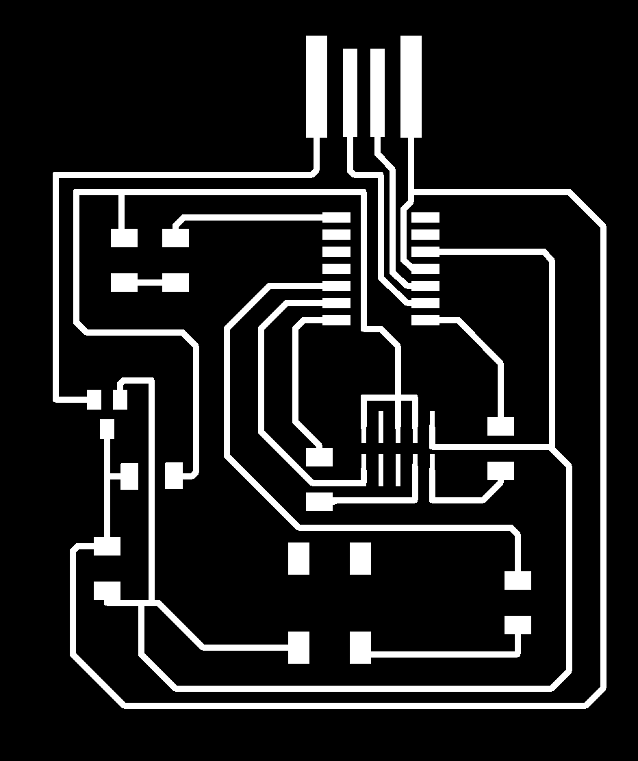
I chose ATSAMD11 to re-drow it.
This is the original ciruit:
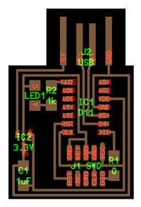
Disgning PCB
Those are the steps I have done:
First, I download fab library where I will find the components needed.
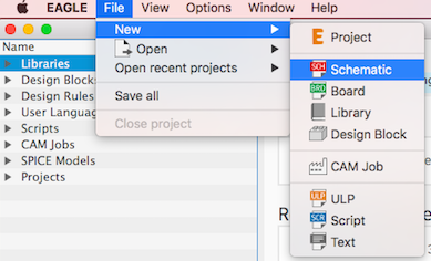
Second/ into eagle software > file > new > schematic
 Then, library > open library manager > in use > browse > the library “eagle fab” > open. Now its installed in eagle.
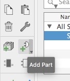
Next, I added the electronics components from this icon in the tool bar;
Then, library > open library manager > in use > browse > the library “eagle fab” > open. Now its installed in eagle.
Next, I added the electronics components from this icon in the tool bar;
 All of the available libraries appeared, I chose eagle fab and started to add the components I need.
I noticed that the IC I need is not available in fab library, therefore I installed anther one that has it.
After that, I started to connect them to each other.
All of the available libraries appeared, I chose eagle fab and started to add the components I need.
I noticed that the IC I need is not available in fab library, therefore I installed anther one that has it.
After that, I started to connect them to each other.
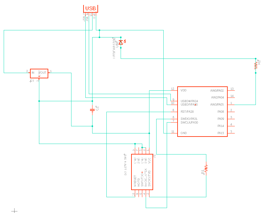 Then I added a LED and a push button.
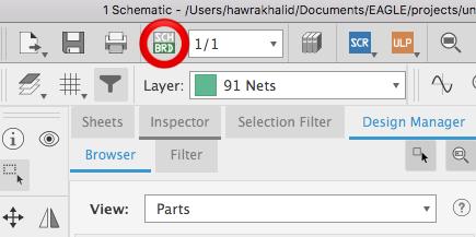
the next step after finishing the schematic is to design the pcb, click this icon;
 It will move you to the desging space.
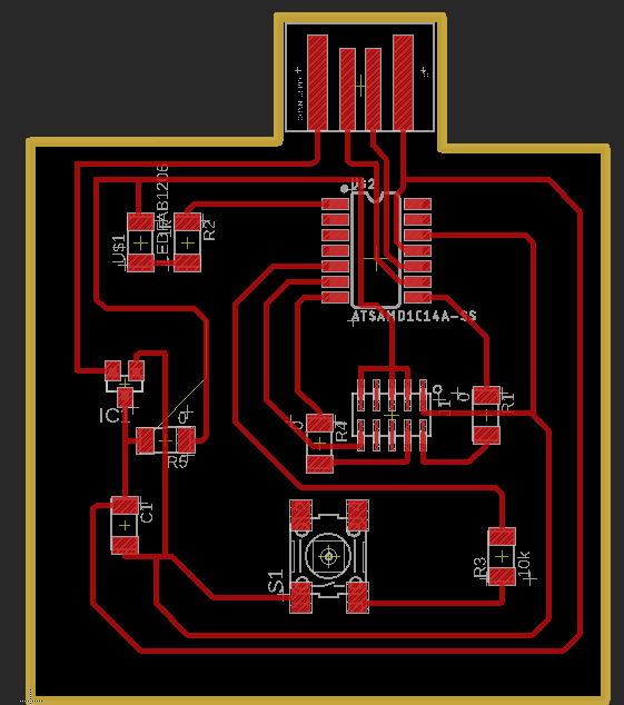
Start to drag and drop the electronics components to the board which is the black area and organize the layout, rotate and put what is connected to each other next to each other, I found that this part is very hard and difficult to me.
I needed to add some jumper resistance and move the components several times.
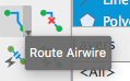
Then rotate the wires with this icon;
It will move you to the desging space.
Start to drag and drop the electronics components to the board which is the black area and organize the layout, rotate and put what is connected to each other next to each other, I found that this part is very hard and difficult to me.
I needed to add some jumper resistance and move the components several times.
Then rotate the wires with this icon;
 It also make it easier because it lights the ones whose connected to each other, and make sure that the width is more than 12.
Thats how it turnes;
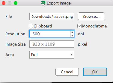
Finally to export the images as traces go to layer setting> hide layers> Top, then click OK.
Now export it file> export > image. and changed the settings as follwing.
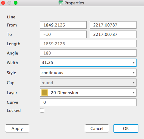
For the outline, make sure that the width is 1/32 inches which equals to 31.25 mils, right click on each line and change them
 then do the same steps above but insteade of showing the top, click “Dimension” then export it.
Milling & Soldering
I export the images into mods and I have done the same steps I did in Electronics production week.
After clicking calculate “to produce the RML file”, I sent the files to the SRM-20 milling machine.
I placed the 1/64 excavator to cut the traces and when its finshed as shown below half of it did not mill well because I did not put an enough support Underneath it.
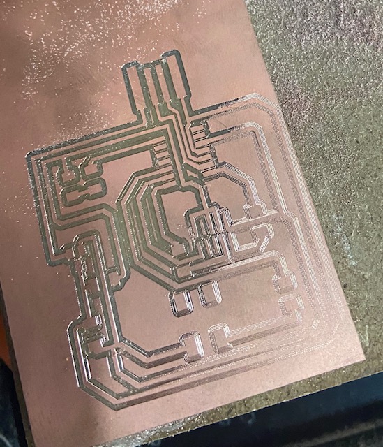
Therefore, I downloaded the excavator a bit more to see if its gonna work.
Apparently it worked except the corner , so I placed some papers underneath the copper hopping that it will work
And finally the circuit milled well
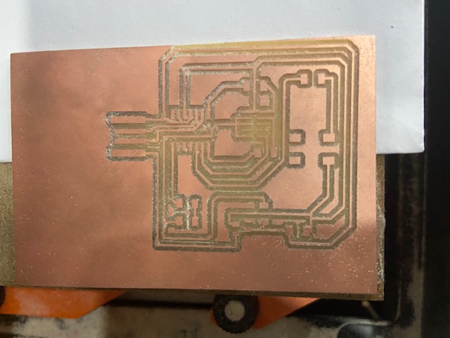
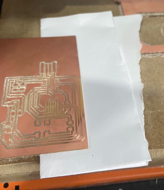
Then, I placed the 1/32 milling bit and mill the outline, and while its milling I prepared the components I need.
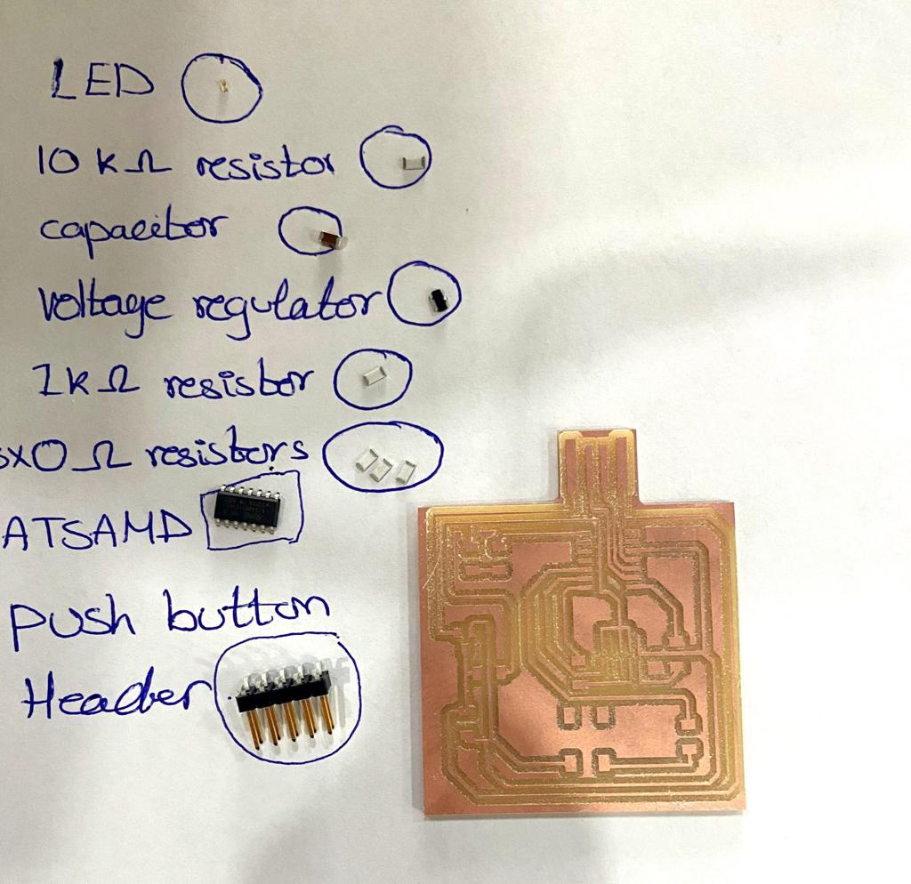
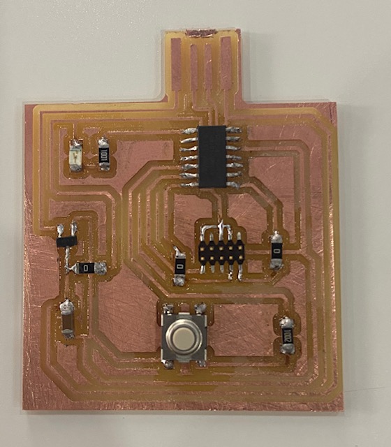
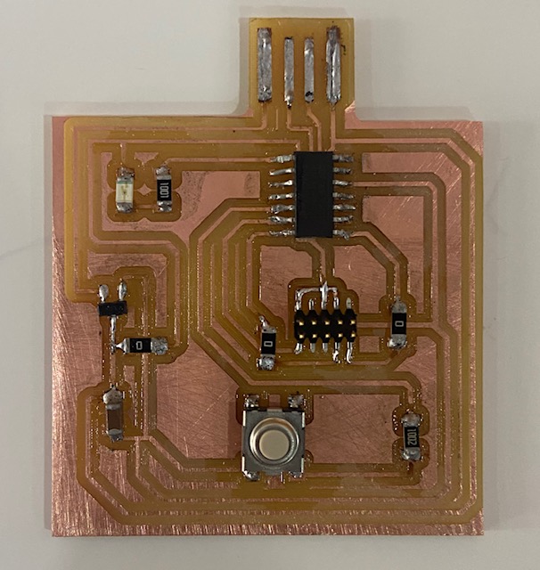
I started soldering the components on my circuit and here the final result
Programming
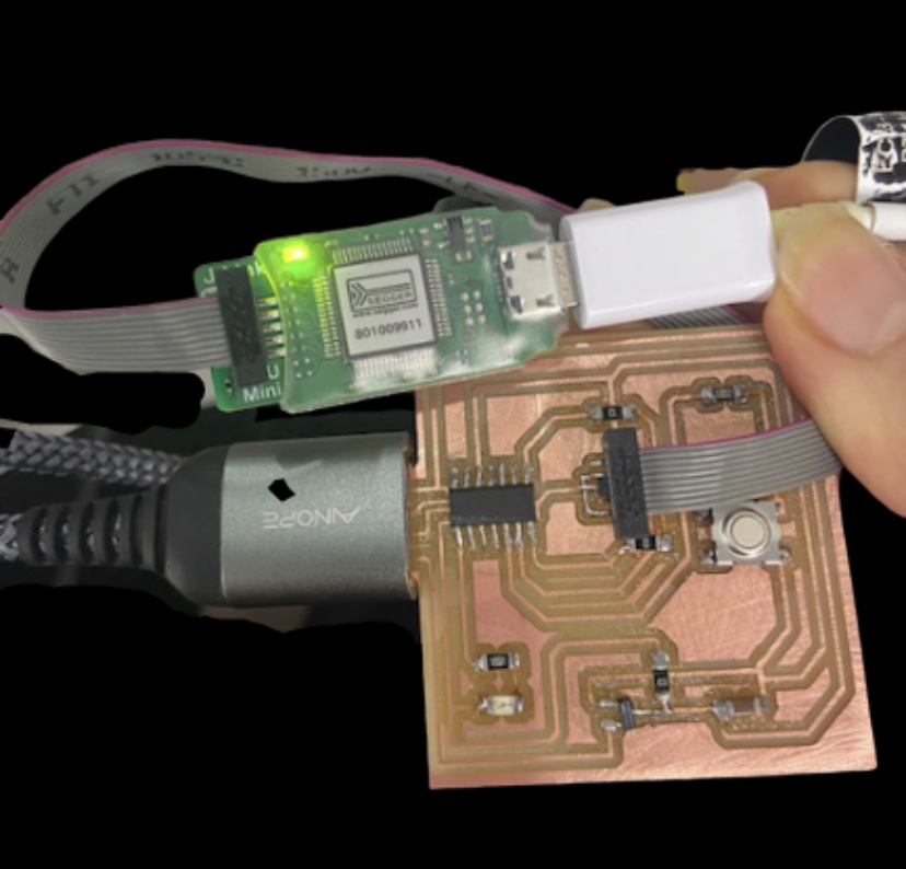
Using Atmel Studio and j-link programer I have done these steps:
-
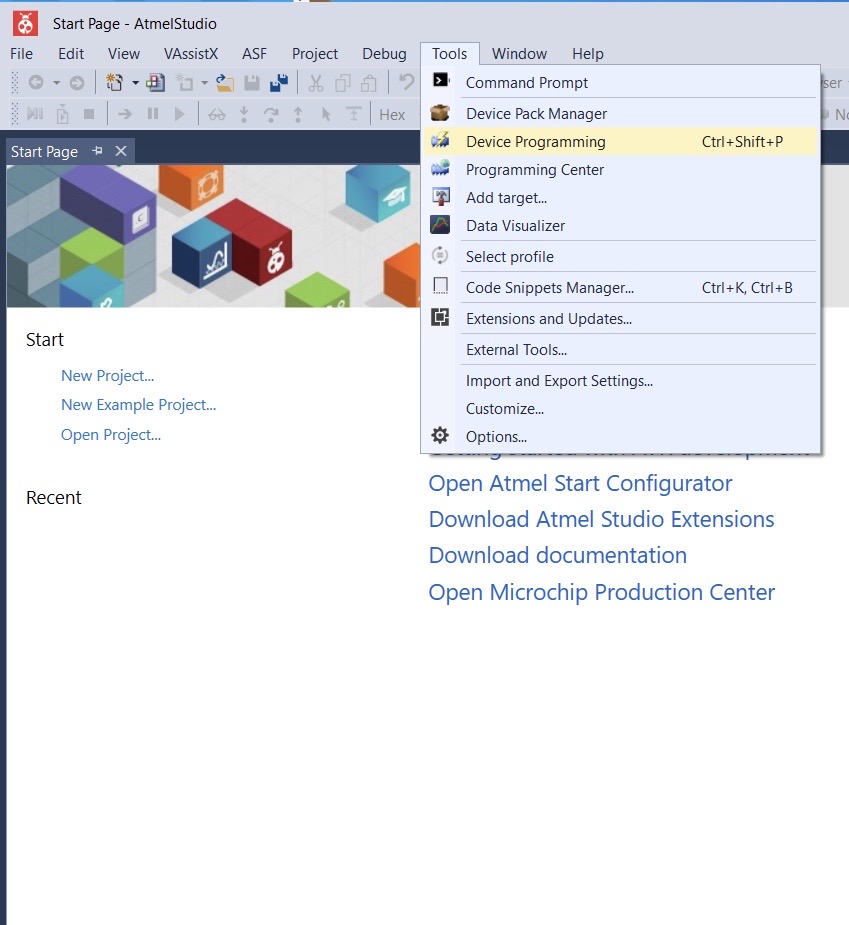
Open atmel studio > tools > Device programming.
-
It will show off an page , chose “J Link” as a tool , and while I’m using “ATSAMD11C” I put it as a device ,then click apply > read
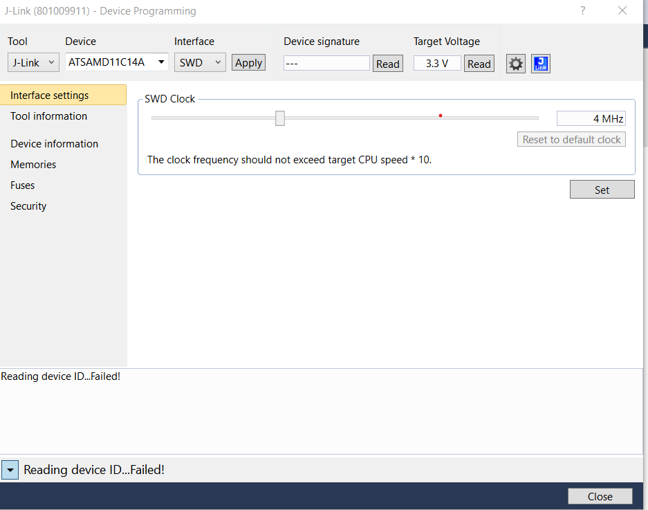
As shown below, an error message appeared
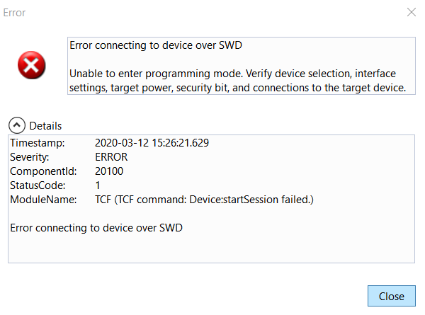
So I re-checked the connection with the voltmeter and found out that I did not soldered the vcc of the header and put some solder in the top.
Then repeated the same steps above and this message appeared
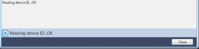
Which means that the circuit could be a programmer succfully.