Embeded Programming
Assignments
So in this week, we are learning about Embeded Programming. So on week 7 , we learn how to make a electronic circuit board. But the board is just for show if there is no program in it. So we code it accoring to its requrements.

So let's meet with Embeded system...
Embeded Systems
An embedded system is a controller programmed and controlled by a real-time operating system (RTOS) with a dedicated function within a larger mechanical or electrical system, often with real-time computing constraints. It is embedded as part of a complete device often including hardware and mechanical parts.
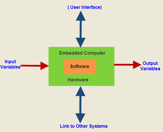
Embedded systems are commonly found in consumer, industrial, automotive, medical, commercial and military applications. (Source:wiki)
Embeded Systems
Microprocessor is an IC which has only the CPU inside them i.e. only the processing powers such as Intel’s Pentium 1,2,3,4, core 2 duo, i3, i5 etc. These microprocessors don’t have RAM, ROM, and other peripheral on the chip. A system designer has to add them externally to make them functional. Application of microprocessor includes Desktop PC’s, Laptops, notepads etc.But this is not the case with Microcontrollers. Microcontroller has a CPU, in addition with a fixed amount of RAM, ROM and other peripherals all embedded on a single chip. At times it is also termed as a mini computer or a computer on a single chip. Today different manufacturers produce microcontrollers with a wide range of features available in different versions. Some manufacturers are ATMEL, Microchip, TI, Freescale, Philips, Motorola etc. Microcontrollers are designed to perform specific tasks. Specific means applications where the relationship of input and output is defined. Depending on the input, some processing needs to be done and output is delivered. For example, keyboards, mouse, washing machine, digicam, pendrive, remote, microwave, cars, bikes, telephone, mobiles, watches, etc. Since the applications are very specific, they need small resources like RAM, ROM, I/O ports etc and hence can be embedded on a single chip. This in turn reduces the size and the cost.
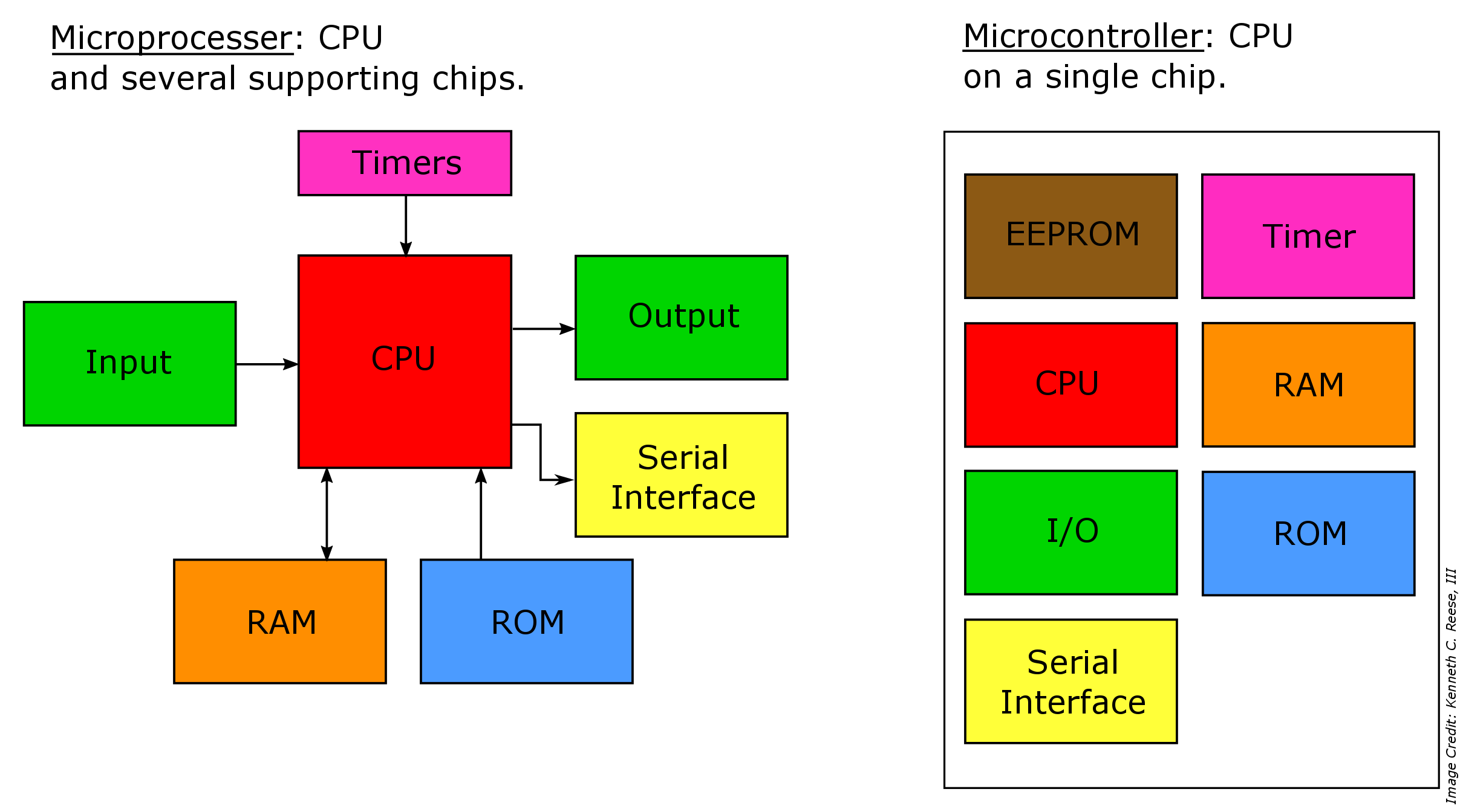
Microprocessor find applications where tasks are unspecific like developing software, games, websites, photo editing, creating documents etc. In such cases the relationship between input and output is not defined. They need high amount of resources like RAM, ROM, I/O ports etc. The clock speed of the Microprocessor is quite high as compared to the microcontroller. Whereas the microcontrollers operate from a few MHz to 30 to 50 MHz, today’s microprocessor operate above 1GHz as they perform complex tasks. (Source:https://www.engineersgarage.com/tutorials/difference-between-microprocessor-and-microcontroller)
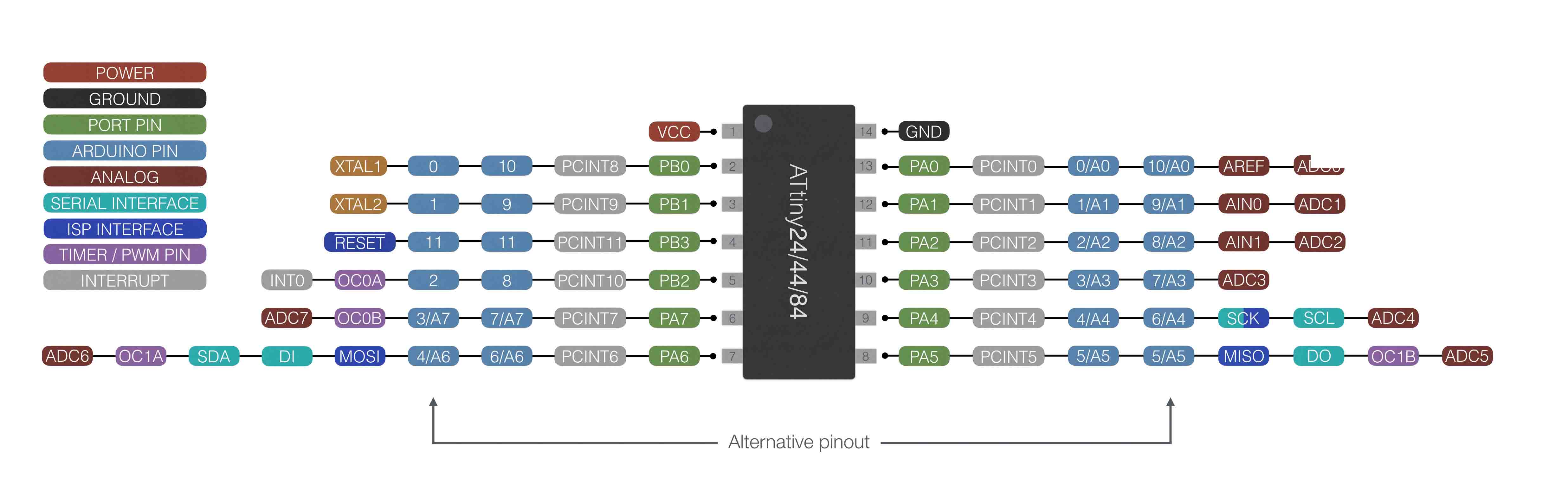
ATTINY 44
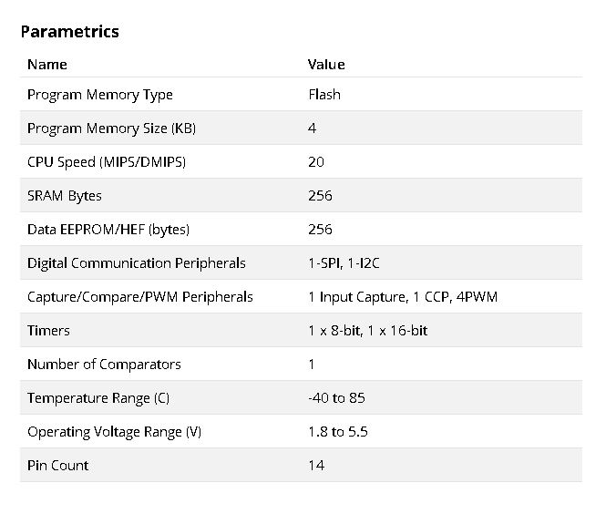
ATtiny (also known as TinyAVR) are a subfamily of the popular 8-bit AVR microcontrollers, which typically has fewer features, fewer I/O pins, and less memory than other AVR series chips. ATTINY 44 is 16 pin 8bit microcontroller.The ATtiny44 is a high-performance, low-power Microchip AVR RISC-based CMOS 8-bit microcontroller.It combines 4KB ISP flash memory, 256-Byte EEPROM, 256B SRAM, 12 general purpose I/O lines .The ATtiny44 consistof 32 general purpose working registers, an 8-bit timer/counter with two PWM channels, a 16-bit timer/counter with two PWM channels, internal and external interrupts, an 8-channel 10-bit A/D converter and a programmable gain stage (1x, 20x) for 12 differential ADC channel pairs. It has a programmable watchdog timer with internal oscillator.The a internal calibrated oscillator and three software selectable power saving modes makes it suitable for small embedded products . By executing powerful instructions in a single clock cycle the device achieves throughputs approaching 1 MIPS per MHz .It also balance power consumption and improve processing speed.
You can read the data sheet Here
These are some basic details about the chip.
Let's check out the black diagram...
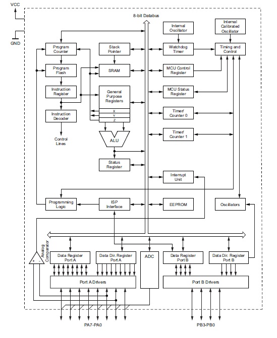
Pin description
Supply voltage.
Ground
Port B is a 4-bit bi-directional I/O port with internal pull-up resistors (selected for each bit). The Port B output buffers have symmetrical drive characteristics with both high sink and source capability except PB3, which has the RESET capability. To use pin PB3 as an I/O pin instead of RESET pin, program (‘0’) RSTDISBL fuse. As inputs, Port B pins that are externally pulled low will source current if the pull-up resistors are activated. The Port B pins are tri-stated when a reset condition becomes active, even if the clock is not running.
Reset input. A low level on this pin for longer than the minimum pulse length will generate a reset, even if the clock is not running.
Port A is a 8-bit bi-directional I/O port with internal pull-up resistors (selected for each bit). The port A output buffers have symmetrical drive characteristics with both high sink and source capability. As inputs, Port A pins that are externally pulled low will source current if the pull-up resistors are activated. The port A pins are tri-stated when a reset condition becomes active, even if the clock is not running
Programming ATtiny44 with ARDUINO IDE
Arduino is an open source computer hardware and software company, project, and user community that designs and manufactures single-board microcontrollers and microcontroller kits for building digital devices and interactive objects that can sense and control objects in the physical and digital world.[wiki]
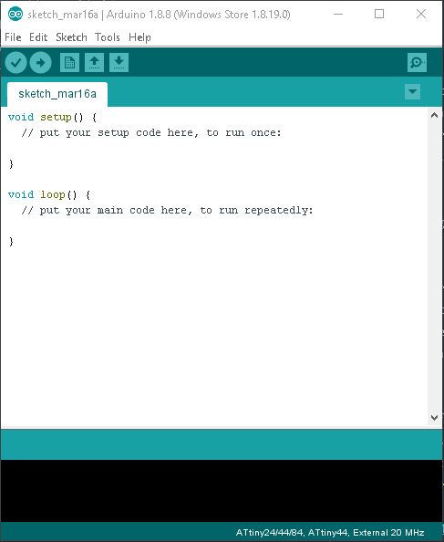
I had some previous experience with adruino, so the processes that are done here is familiar to me. Arduino IDE can be downloaded from Online. Open it and you can see following window
The original arduino software does not support Attint series. So we have to add some udates for that. Go to "file" and click "preference"
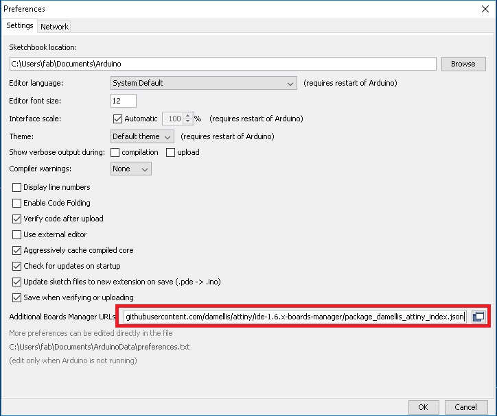
Add following address to the "Additional Board Manager URL"
https://raw.githubusercontent.com/damellis/attiny/ide-1.6.x-boards-manager/package_damellis_attiny_index.jsonclick "OK"

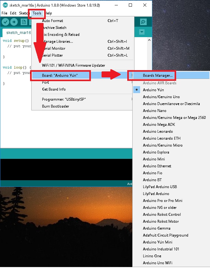
Now to set up the attiny boards, Go to "Tools". Then you can see "Boards". Then click "Board Manager"
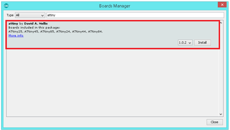
Now search for attiny file in the manager
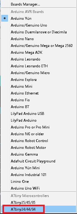
Now you can select ATtiny44 under the ATtiny Microcontrollers in board Selection
We are using the "Fab ISP" wee made in week 5 to program "Echo Hello World" board that we made in week 7 . For that select"usbtiny" under "Tools" to "Programmer"
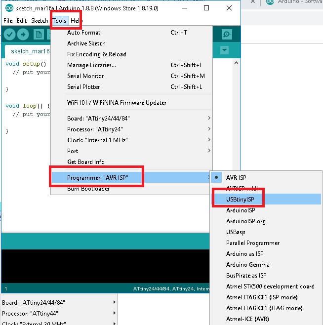
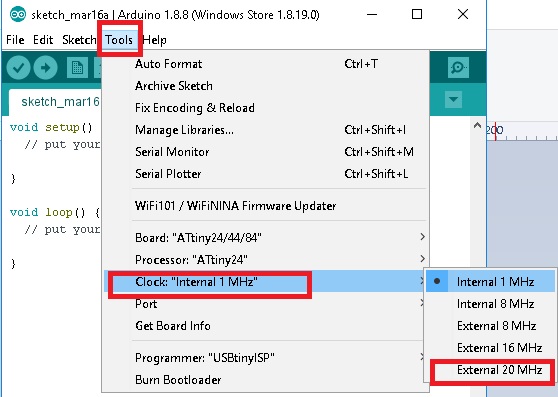
Arduino runs on 1MHz clock. But "Echo Hello World"works on 20MHz.So go to "Tools" then select "Clock" to "20MHZ"
Arduino Code
Here is the code that I used for the board;
int led = 7;
int btn = 3;
int val = 0;
void setup()
{
pinMode(led,OUTPUT);
pinMode(btn,INPUT);
}
void loop(){
if (digitalRead(btn) == LOW) { // check if the input is HIGH (button released)
digitalWrite(led, HIGH); // turn LED On
} else {
digitalWrite(led,HIGH);
delay(100);
digitalWrite(led,LOW);
delay(100);
}
}
Copy and paste the code into Arduino IDE. The main buttons on top are listed below. Save and varify the the code for errors
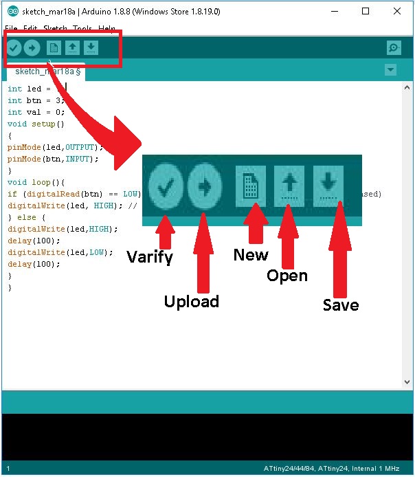
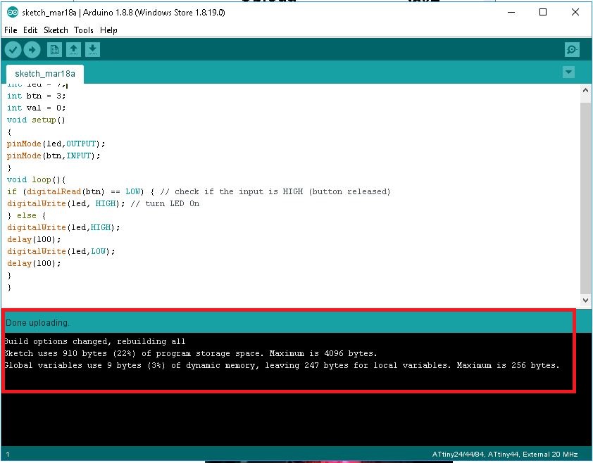
After varification, upload the code into the hello-world-board.
Normal
Push-Button
Programming ATtiny44 using ATMEL STUDIO
Studio 7 is the integrated development platform (IDP) for developing and debugging all AVR® and SAM microcontroller applications. The Atmel Studio 7 IDP gives you a seamless and easy-to-use environment to write, build and debug your applications written in C/C++ or assembly code. It also connects seamlessly to the debuggers, programmers and development kits that support AVR® and SAM devices.

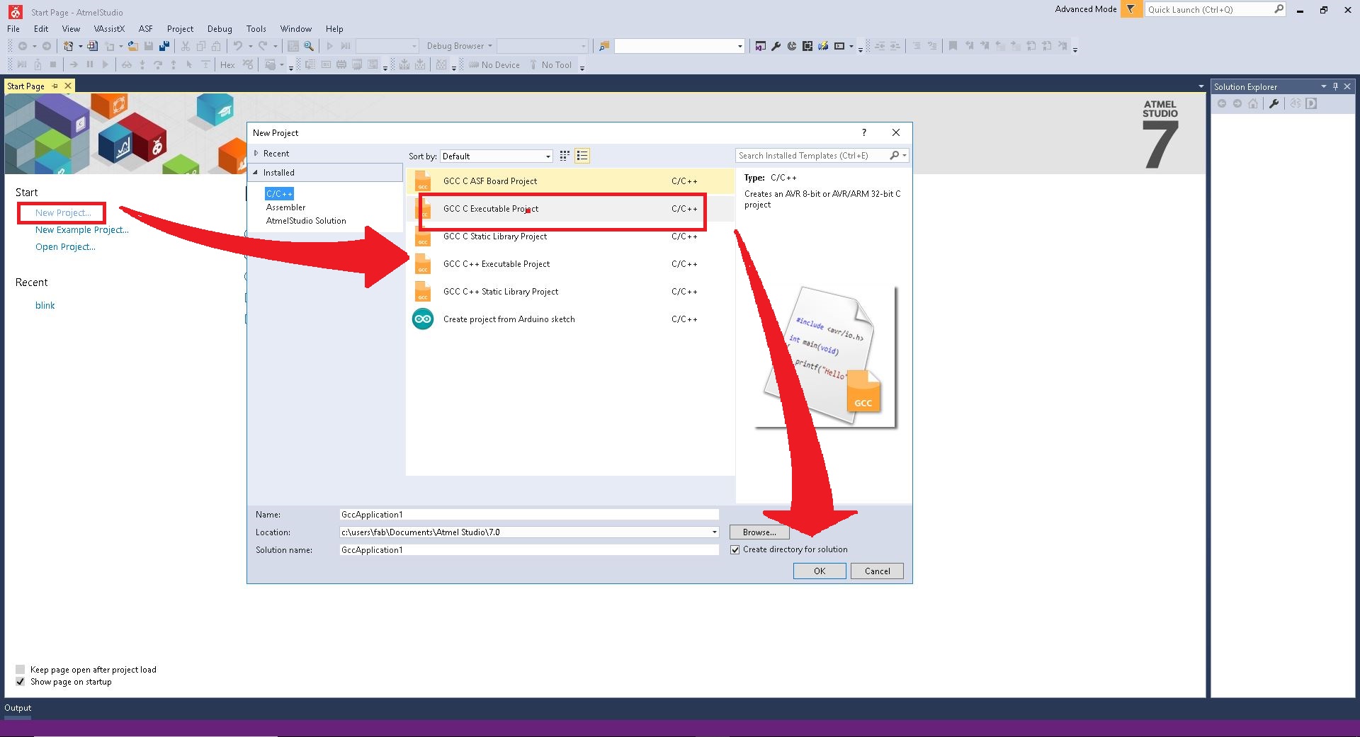
For programming first install and open ATMEL STUDIO. Click "New Project" and srlect"GCC C Exictable project". Click ok to confirm the selection
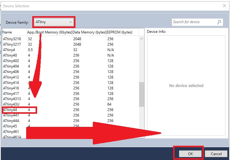
Now you can see the following window. Select device famiy as Attiny and select Attint 44. Click ok to confirm the operation.
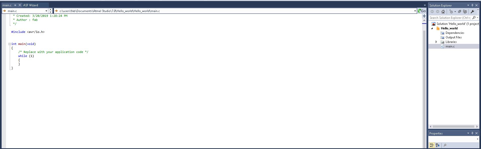
Now you will get a window like below
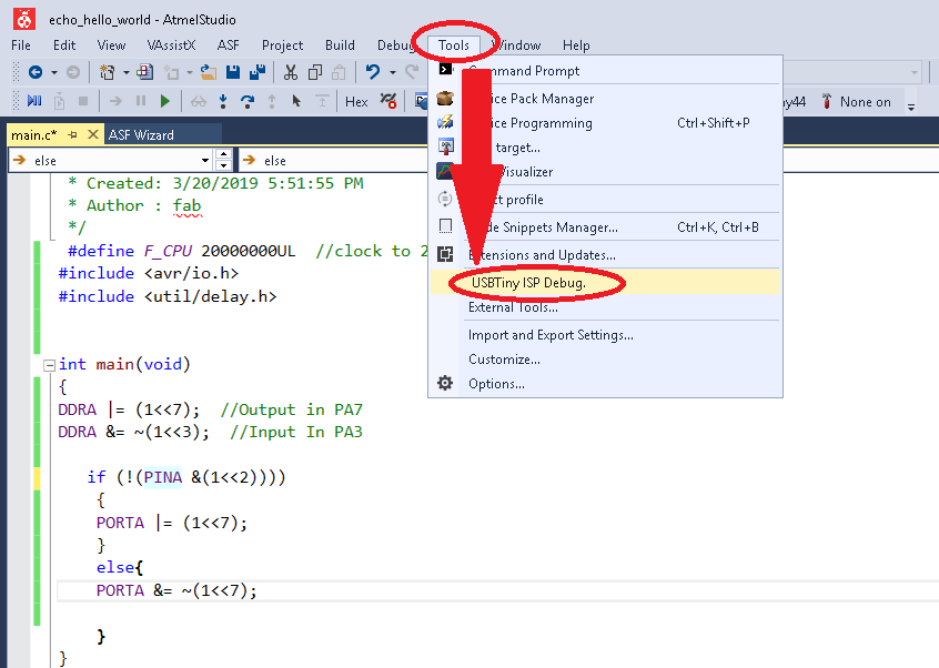
Now we need to setup some parameters for usbtiny debugging. For that Go to "Tools" and Select "External Tools..."
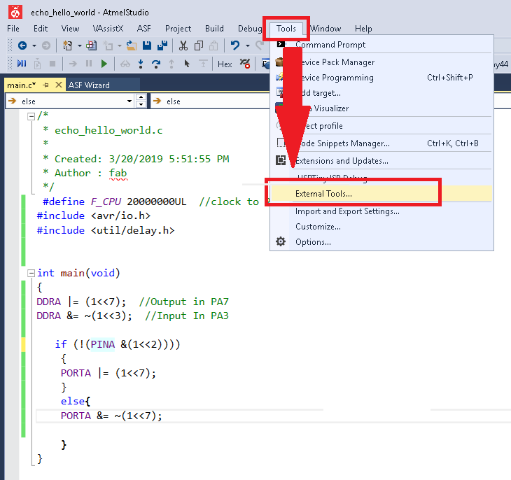
Add following details to the box:
Title:- USBTiny ISP Debug
Command :- avrdude.exe
Arguments :- -c usbtiny -p attiny44 -U flash:w:$(ProjectDir)Debug\$(TargetName).hex:i
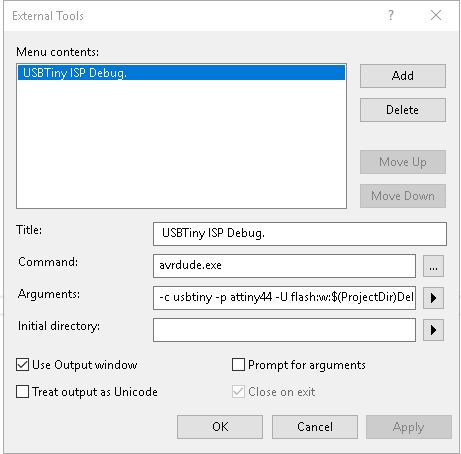
Click "Apply" and "Save" tools. Now add the folling code to the editor:
Now for testing the board, Open "Build" from the menu and click "Build solution"
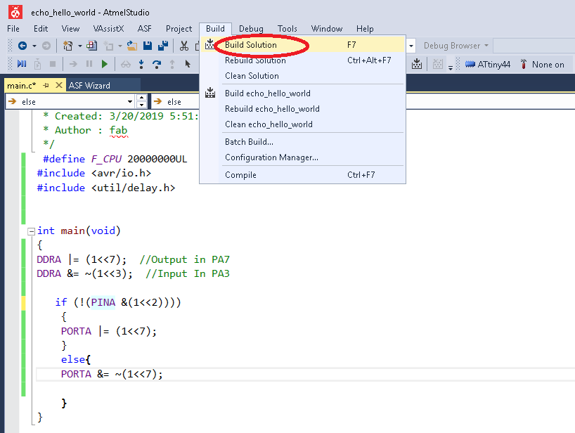
Now it is compailed. We have to upload into the board. For that go to "Tools" again and click "USBTiny ISP Debug":
Here is the code
/*
 *echo_hello_world.c
 *
 * Created: 3/20/2019 12:12:37 PM
 * Author : Fab
 */

#define F_CPU 20000000UL  //clock to ppppp
#include <avr/io.h>
#include <util/delay.h>


int main(void)
{
DDRA |=(1<<7);  //Output in PA7
DDRA |=(1<<3);  //Iutput in PA3

      if (!PINA &(1<<2))))
     {
    PORTA |= (1<<7);
     }
      else{
        PORTA &= (1<<7);
     }
}
Now we get the same result
Normal
Push-Button
Experiment with other architectures
In this week group assignment is to try out some other acchtecture other than AVR microcontrollers.
ARM (Advanced RISC Machines)
y now, there would be a very small segment of the mobile community that would not have heard anything about the Android OS by Google. This OS seems to be giving many proprietary vendors a run for their money and the owners many a sleepless nights. But did you know as to what does android depend on for its good performance apart from its robust code? What makes it run so smooth and yet amazingly fast without costing you a fortune? What drives the Android? The answer is ARMs, Advanced RISC Machines, previously known as Acorn RISC Machines.
ARM machines have a 32 bit Reduced Instruction Set Computer (RISC) Load Store Architecture. (Also read article on CISC & RISC Architecture) The relative simplicity of ARM machines for low power applications like mobile, embedded and microcontroller applications and small microprocessors make them a lucrative choice for the manufacturers to bank on. The direct manipulation of memory isn’t possible in this architecture and is done through the use of registers. The instruction set offers many conditional and other varieties of operations with the primary focus being on reducing the number of cycles per instruction featuring mostly single cycle operations.
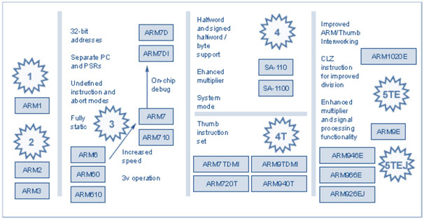
All instructions in the ARM ISA are conditional with the normal execution instructions also being accompanied by condition AL. There are 14 conditions available excluding AL. The instruction set added many feathers to its cap as and when the generations grew. The transistor count has also increased substantially from 30000 in ARM2 to about 26 million in Cortex-A9 ARM. An additional Thumb architecture was developed to support 16-bit instruction models on the otherwise 32 bit ARM machines. No matter the added advantage of increased code density which was about 65% of the original ARM code, this resulted in a little performance drop in the ARM machines. This drop was somewhat balanced with Thumb 2 which was a major extension over the Thumb ISA.
ARM Architecture Contd.
In Thumb 2, the compiler automatically selects a mixture of 16 bit and 32 bit instructions. It is to be noted that only the instruction set changes from 32 bit to 16 bit, the core continues to operate at 32 bit. The evolution of ARM v7 cores saw the development of Thumb Execution Environment (Thumb-EE) which offered dynamic coding by compiling the code moments before or during execution itself. Thumb feature is basically another Instruction Set running on the same platform. Another Instruction set, to execute Java codes on ARMs was developed soon and was named Jazelle. These three Instruction sets are now the three states on an ARM core and to shift from one state to another, directives like ARM, THUMBX and THUMB are given to the assembler. The evolution of ARM architectures is shown in the figure below:
The nomenclature of ARMs is based on the type and features used in it. For example in ARM7TDMI, ‘T‘ stands for Thumb, ‘D’ and ‘I’ together comprise the on chip debugging facilities and ‘M’ signifies support for an enhanced multiplier and support for 64-bit results. ARMx7z like the ARM1176JZ-S indicates AXI bus, physically mapped caches and MMU, has version 6Z architecture. In this way, there is a naming convention for ARM devices.
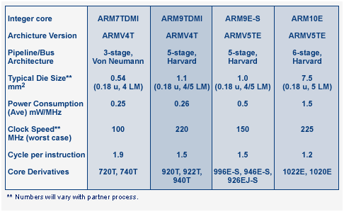
ARM architectures used various stages of pipelining to enhance the flow of instructions to the processors. This allows several operations to be performed simultaneously which would otherwise be performed serially. For example, the ARM7TDMI used 3 stages, ARM9TDMI uses 5 stages and the ARM10TDMI use 6 stages of pipeline to speed up delivery and faster clocking. Cores up to ARM7 followed a Von Neumann type architecture which is essentially memory mapped architecture. ARM9 and its successors shifted to Harvard Architecture which is port mapped. They also provide a robust debugging environment like the Embedded ICE Logic which connects with the external world through a Test Access Port or a standard IEEE 1149.1 JTAG connection. This helps shorten the development cycle.
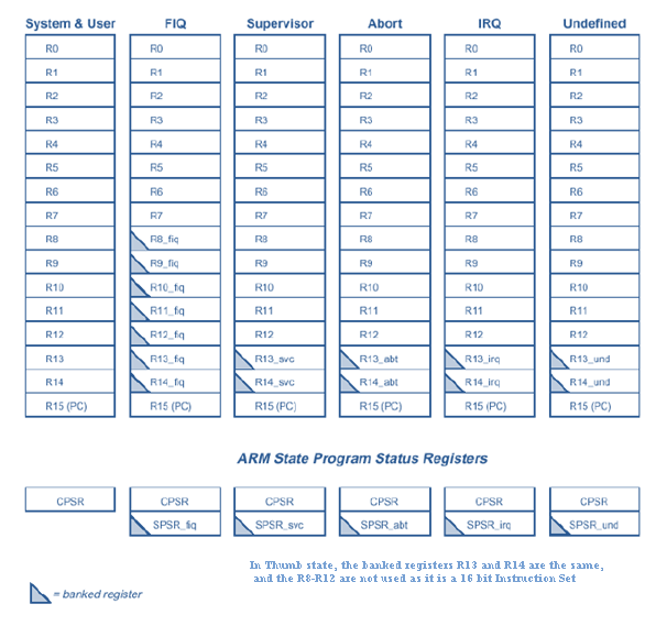
ARM Registers
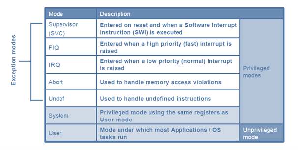
In general ARMs have 37 registers arranged in partially overlapping banks, with separate register banks for each processor mode thus providing rapid context switching for special operations. The various modes in an ARM can be summarized in the figure below.
Each register is 32 bits in size.
The registers are roughly divided into:
Classification of Instruction Set
The ARM and Thumb instruction sets can be broadly classified into the following functional groups.
Source:https://www.engineersgarage.com/articles/arm-advanced-risc-machines-processors
STM32
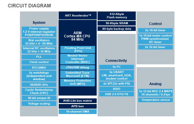
STM32 is a family of 32-bit microcontroller integrated circuits by STMicroelectronics. The STM32 chips are grouped into related series that are based around the same 32-bit ARM processor core, such as the Cortex-M7F, Cortex-M4F, Cortex-M3, Cortex-M0+, or Cortex-M0. Internally, each microcontroller consists of the processor core, static RAM memory, flash memory, debugging interface, and various peripherals.
In here Fablab Kochi we have the STM32F401 series Nucleo development boards.it's a part of the STM32 Dynamic Efficiency™ device range. These devices offer the best balance of dynamic power consumption (in run mode) and processing performance, while integrating a high number of added-value features in packages as small as 3 x 3 mm.
The MCUs deliver the performance of Cortex®-M4 core with floating point unit, running at 84 MHz, while achieving outstandingly low power consumption values in run and stop modes.
- Performance: At 84 MHz, the STM32F401 delivers 105 DMIPS/285 CoreMark performance executing from Flash memory, with 0-wait states using ST’s ART Accelerator. The DSP instructions and the floating point unit enlarge the range of addressable applications.
- Power efficiency: ST’s 90 nm process, ART Accelerator and the dynamic power scaling enables the current consumption in run mode and executing from Flash memory to be as low as 128 µA/MHz. In Stop mode, the power consumption can be as low as 9 µA.
- Integration :The STM32F401 portfolio provides from 128 to 512 Kbytes of Flash, 96 Kbytes of SRAM. The available packages range from 49 to 100 pins.
- 3x USARTs running at up to 10.5 Mbit/s,
- 4x SPI running at up to 42 Mbit/s,
- 3x I²C,
- 1x SDIO,
- 1x USB 2.0 OTG full speed,
- 2x full duplex I²S up to up to 32-bit/192KHz,
- 12-bit ADC reaching 2.4 MSPS,
- 10 timers, 16- and 32-bit, running at up to 84 MHz
You can Download the Sheet from here