Week 7: Electronic Design
Objectives
Learning Outcome
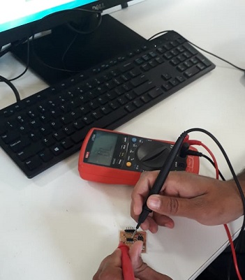
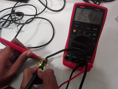
This week's group assignment was to use the test equipment in our lab to observe the operation of a microcontroller circuit board. In order to test the designed microcontroller circuit board we used digital equipments for example multimeter and oscilloscope. By Using digital multimeter we tested continuity , voltages and resistance of components. We also checked the led polarity using multimeter.
Group Assignment
In our lab we have available two types of digital multimeter.
1. UT33C
2. DMM 8061
Continuity check of components.
Voltage check across Attiny 44.
In begining I did my group assignment with my fabmates Azmat, Tariq, Ali raza and Ali Haider. Later I did individual assignment which was to redraw the echo hello board and add at least one button and led. First step for that was to download and install the cad software for pcb designing. There were many like Kicad, proteus and eagle. I used eagle software for my echo hello board because it is versatile. Furthermore in order to mill my designed zee Pcb I repeated all of the steps learnt in fourth week of electronics production. It was really nice to work in this week.
Individual Assignment
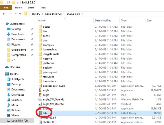
The eagle software uses libraries for different components so for fab ehcho hello board I needed to download fab library which i downloaded from tutorial link. Later we need to paste this library to the eagle file where it is installed. The snap shows below that fab library is pasted in location of eagle software.
After Saving it to location now open the software and do following steps.
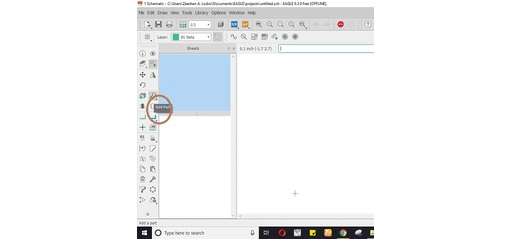
Step 1. I created new file (File => new => schematics).
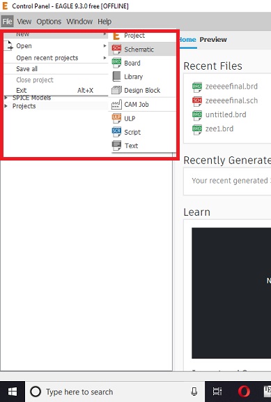
Step 2. I added fab library
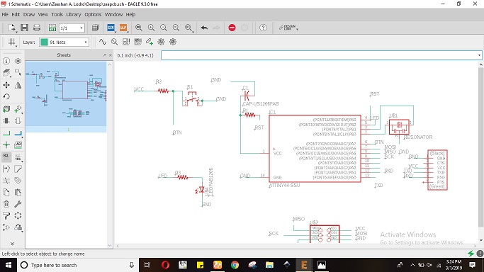
Step 3. In order to design schematics of Echo hello world board I choose following components with fingerprint.
1) Attiny 44.
2) Resistor.
3) Capacitor.
4) LED.
5) SMD Header.
6) Resonator
7) Push Button.
8) Isp Header
All of the connections should be done according to provided board. For led and button connections I followed nadir's fabpage.
Step 4. After making schematics I went to file and clicked switch to board which asked me to create new file from schematics. After saying yes it took me to pcb design file.
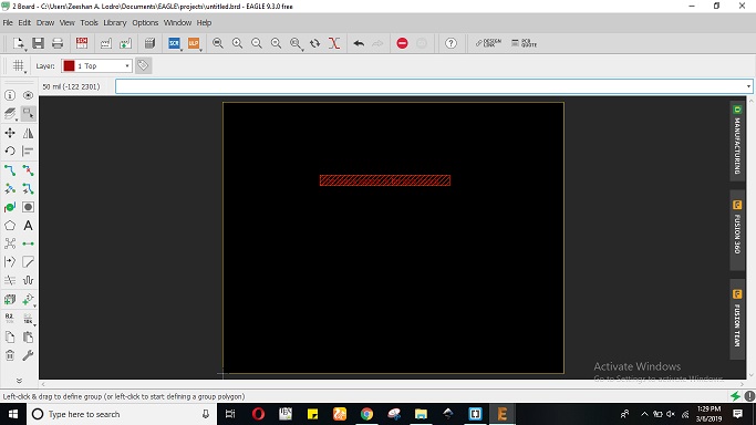
Step 5. Now by using few commands like group, move, rotate and route I arranged my components in a desired shape. Few things should be considered while routing that board. make angles of connections equal to 45 or 60 and less than 90. make trace width atleast 0.012. try to keep distance between connections because they might get short and your board may not work.
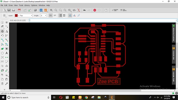
Step 6. I did DRC rule check just to know the errors in board if any. The figure below shows the drc check of my designed board where I found almost 8 errors of air wires which I resolved one by one.
.png)
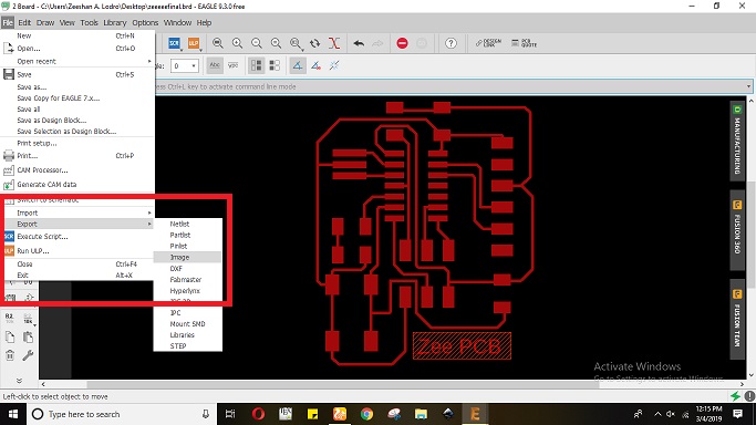
Step 7. It's time to export the designed board as monochrome type image with pixel density of 2000 dpi. Please hide all layers, go to layer setting =>click hide layers=>click top layer before exporting the monochrome image.
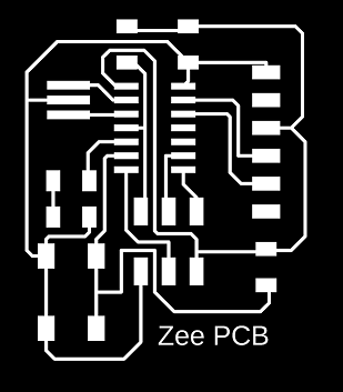
Step 8. The monochrome exported image is shown below.
Step 9. Now echo hello world board is ready. In order to mill this board I needed to make it's rml files using fab mods or cba mods. I repeated all of the steps of fourth week. The below fig shows the generated rmls of board.
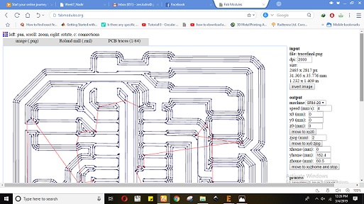
Step 10. Now I needed to fabricate the ftdi hello board using srm 20 machine. The output can be seen below
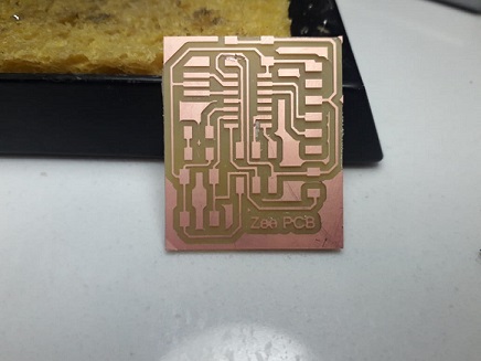
Step 11. After milling the board I needed to solder the required components. I picked up following components from fablab kahirpur inventory.
1) Attiny 44 (01).
2) Resistor (10 Kilo Ohm =>02 and 499 Ohm => 01).
3) Capacitor (10 uf).
4) LED (green colour).
5) SMD Header (6 pin).
6) Resonator (20 MHz)
7) Push Button (01).
8) Isp Header (6 pin)
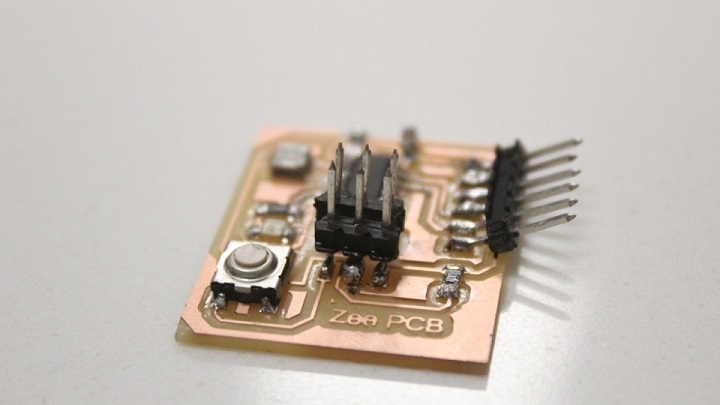
I soldered all of the componets very carefully. My soldered zee pcb can be seen below