
Week 1: Principles and Practices
Objective
Learning Outcome
Final Project Thoughts
Initially I searched number of projects using fab search engine where I found many display projects for example Lixie display, cubic display and ilusion mirror. All in all I found a project idea given by Mr Christian Cardenas of crystal structures. After thinking alot I realized that their should be a device which shall help students to imagine the nano structures. Basically We have learnt a course of nano technology in which we were taught about nano 3D cubic lattice structures which were hard to imagine and understand in short time. Therfore idea is that to build a 6x6x6 digital latice cube which print all chemical cubic structures, mathematical cubic structures etc.
Introduction to Solids
The outstanding macroscopic properties of crystalline solids are rigidity, incompressibility and characteristic shape. All crystalline solids are composed of orderly arrangements of atoms, ions, or molecules. Furthermore macroscopic result of the microscopic arrangements of the atoms, ions or molecules is exhibited in the symmetrical shapes of the crystalline solids. Solids are either amorphous, without form, or crystalline. In crystalline solid s the array of particles are well ordered. Crystalline solids have definite, rigid shapes with clearly defined faces. The arrangement of the atoms, ions or molecules are very ordered and repeat in 3-dimensions. Small, 3-dimensional, repeating units called unit cells are responsible for the order found in crystalline solids. The unit cell can be thought of as a box which when stacked together in 3-dimensions produces the crystal lattice. There are a limited number of unit cells which can be repeated in an orderly pattern in three dimensions.
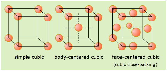
The basic cubic lattice structures are categorized as given
1. Simple cubic structure
2. Body centered cubic struccture
3. Face Centered structure
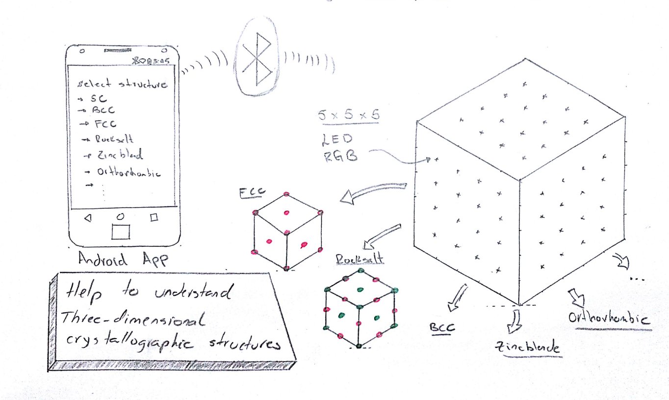
First Sketch
Initially I want to detect any crystall material which should have cubic structure. After detection of that structure it will be shown on digital atomic cube. Almost all of cubic structures will be predefined in a mobile app which shall direct the structure via Wifi or blutooth module to digital atomic cube. After receiving the command the specified leds light up for example if we have a cubic crystal structure then corner leds shall be lighten up in a red colour while others should be in blue colour.
Add on: If I succeeded in project I may record human voice, convert it to particular pattern and print it on digital atomic cube with frequency and pitch of voice for example if your voice is heavy then it shows your voice pattern like that given below.
To Coverup the project I need following skills to learn.
Few components which I shall buy.
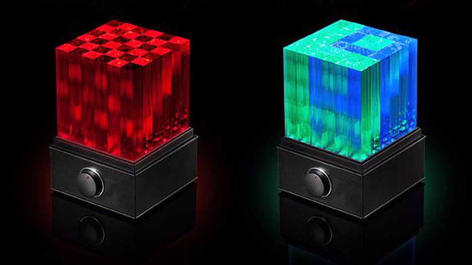
The final model will some how look like this.
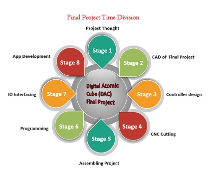
Project TimeLine
What It will do?
It will print the crystallographic structure taught in nano technology course or chemistry. The crystallographic structures like simple cubic, face centered, orthorhombic and salt etc will be printed on this cube just to imagine the structures easily
Where I will use this?
In higher secondary education students are very confused while imagining the 3D structures. In order to increase imaginative power this device works superbly for student where they can imagine all 3D structures at cheep cost. This device could be used in all educational institutions wherever 3D stuctures are taught specifically chemistry or nano electronics.