group assignment here
Electronics Production
Group assignment : Characterize the design rules for your PCB production process
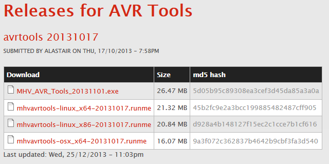
MACHINE WE USE
Roland monoFab SRM-20
relevant technical data fom roland web page
roland web page
Cuttable Material Modelling Wax, Chemical Wood, Foam, Acrylic, Poly acetate, ABS, PC board
X, Y, and Z Operation Strokes 203.2 (X) x 152.4 (Y) x 60.5 (Z) mm
Workpiece table size 232.2 (X) x 156.6 (Y) mm
Distance From Collet Tip to Table Max, 130.75mm (5.15 in)
Loadable Workpiece Weight 2 kg (4.4 lb)
X-, Y-, and Z-Axis Drive System Stepping motor
Operating Speed 6 - 1800mm/min 0.24 - 70.87inch/min
Software Resolution 0.01 mm/step (RML-1), 0.001mm/step (NC code) 0.000039 inches/step (RML-1), 0.000039 inches/step (NC code)
Spindle Rotation Speed Adjustable 3000 - 7000 rpm
Milling tools diameter:
1/64" = 0.015625 in = 0.397 mm
1/32" = 0.03125 in = 0.794 mm
1/16" = 0.0625 in = 1.588 mm
.png)
.jpg)
.jpg)
.jpg)
.jpg)
.jpg)
.jpg)
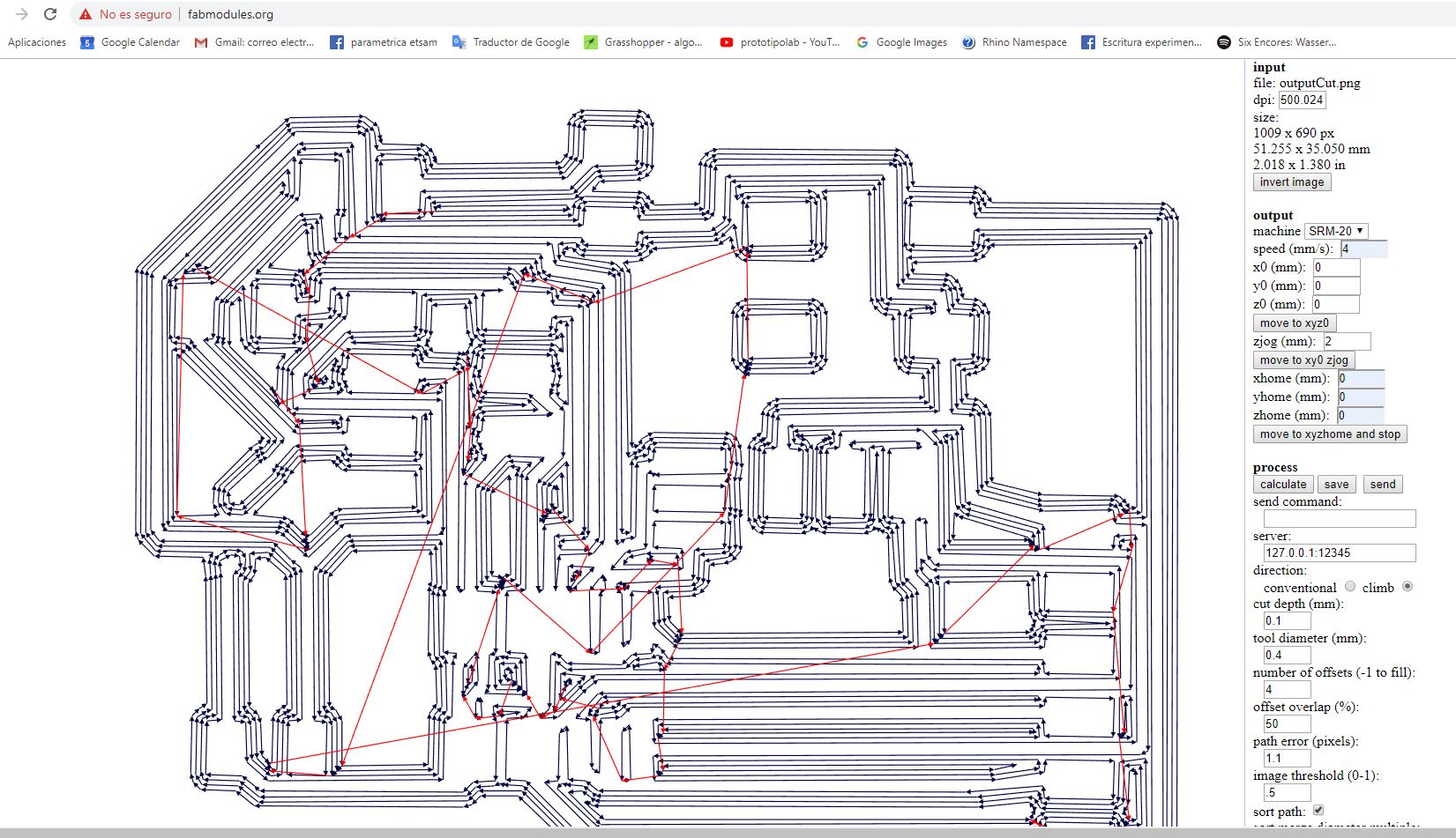
using this parameters:
speed(mm/s): 4
cut depth(mm): 0.1
tool diameter(mm): 0.4
number of offsets(-1 to fill): 4
offset overlap(%): 50
path error(pixels): 1.1
image threshold(0-1): 0.5
.jpg)
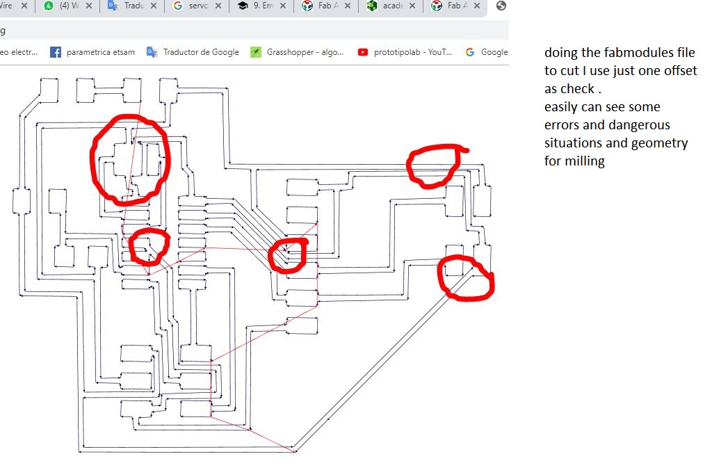
TEST PATTERN OBSERVATIONS
At the beginning of this test, most of the tools were broken in the first attempts to record the test. Thus most of the tests are made with tools whose head has a V-termination. This causes that at a greater depth of engraving the width of the
plot increases beyond the nominal width of the tool.
In the different attempts, it is first tested with successive passes, increasing the Z as engraving depth from -0.02 to -0.05 mm (each with the corresponding offset designated in fab
modules) and later a single pass was attempted with Z between -0.05 and -0.07 mm since there was no fear of breaking the tool.
Since this test is made for the subsequent engraving of lines in the different circuits we look especially at the separation between lines and the thickness of these. In the separation between lines there is no problem in general in the tests
since taking into account the deformation produced by the termination in v of the tool tends to a greater separation. However, special care is taken in the width of the lines to be drawn from 0.04 mm. Below thickness it is possible that the
line is lost
SOLUTION for the different engraving depths
.jpg)
.jpg)
.jpg)
.jpg)
.jpg)
.jpg)
.jpg)
.jpg)
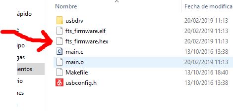
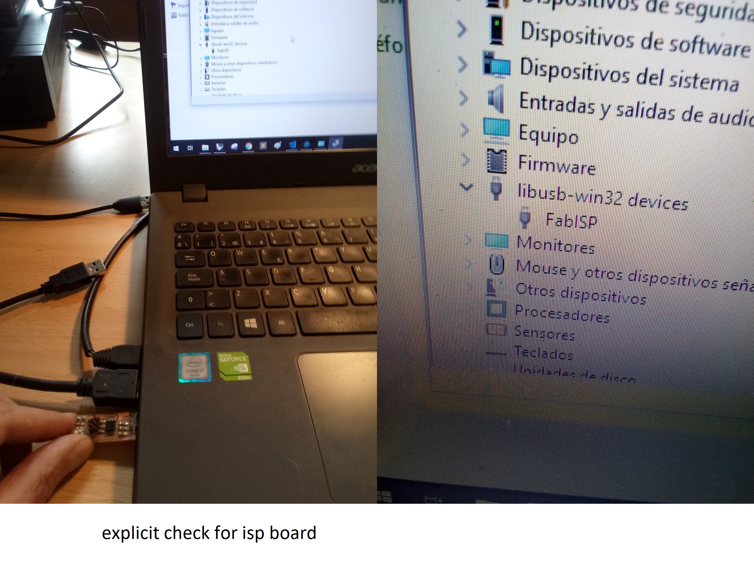
missing process
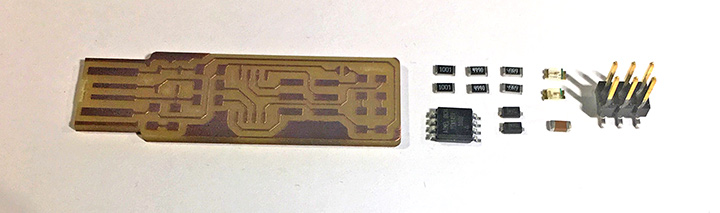
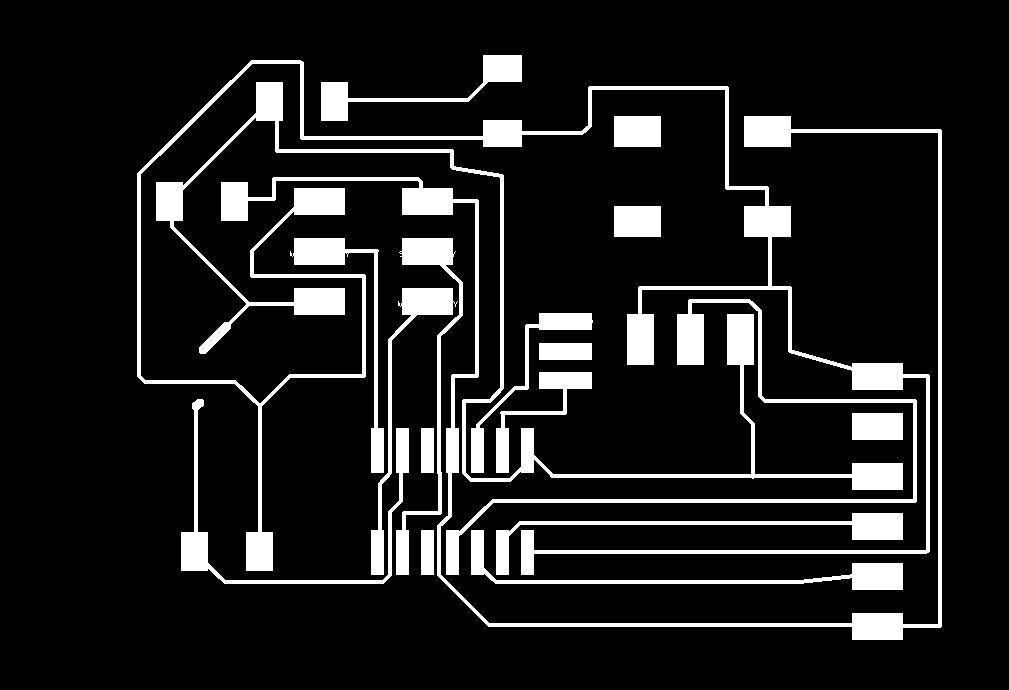
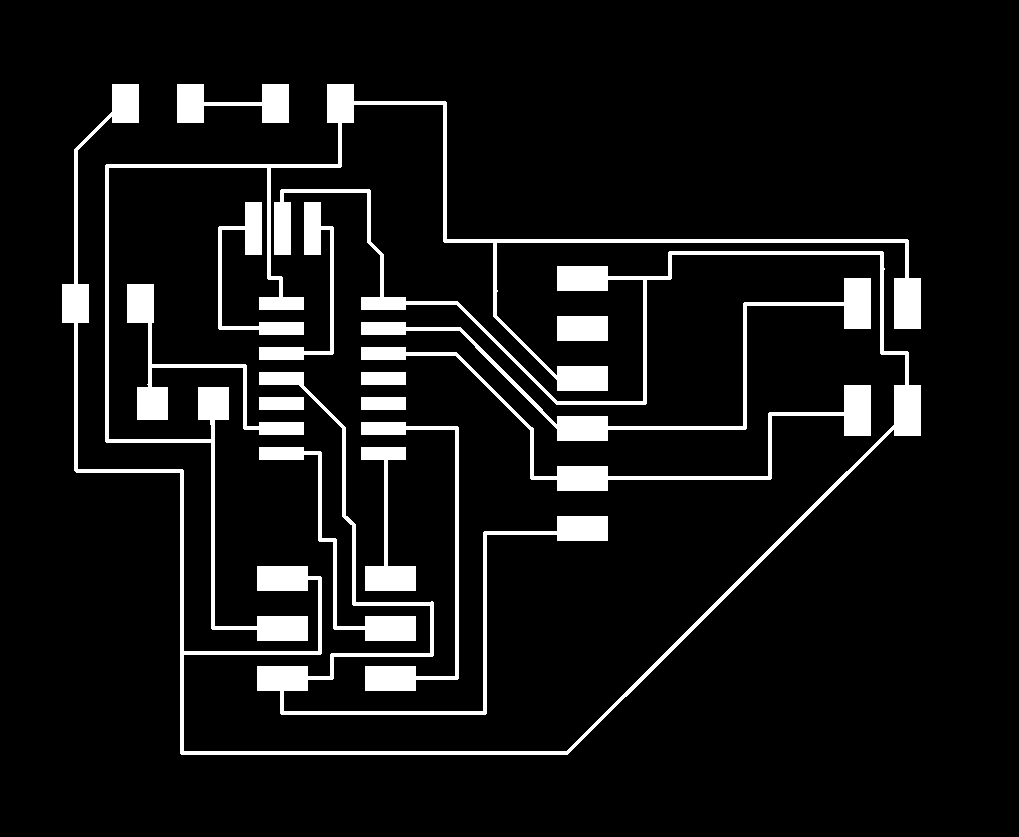
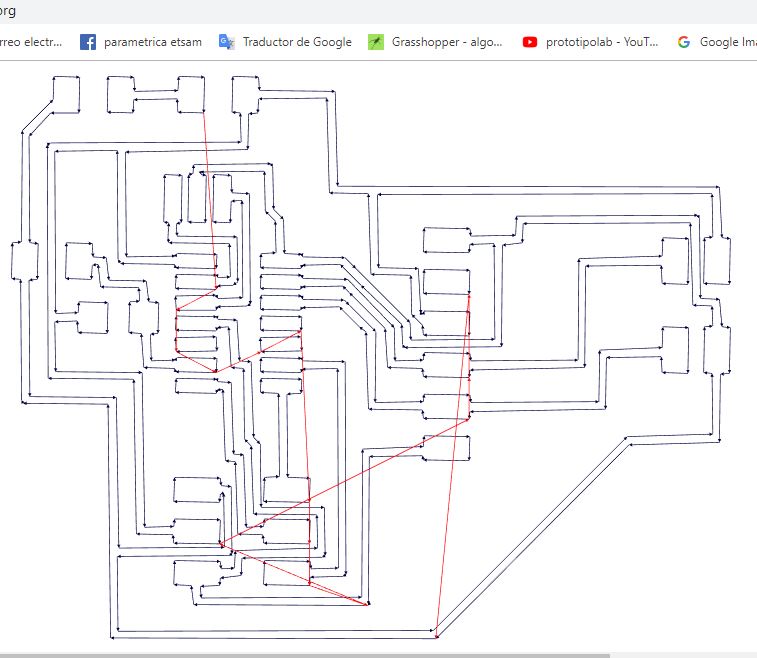
output board for complete milling process
.jpg)
this board has been milled with the next configuration in fab modules:
milling :
tool : 0.4 mm
speed : 3 mm/s
cut deph = 0.1 mm
first check lines for cutting : 1 offset
final configuration for cutting : 3 offset
cutting:
speed : 0.5 mm/s
offsets : 3
.jpg)
.jpg)
.jpg)
.jpg)
.jpg)
.jpg)
.jpg)
.jpg)
.jpg)
.JPG)
.JPG)
.JPG)
.JPG)
.jpg)
.jpg)
.jpg)
.jpg)
.jpg)
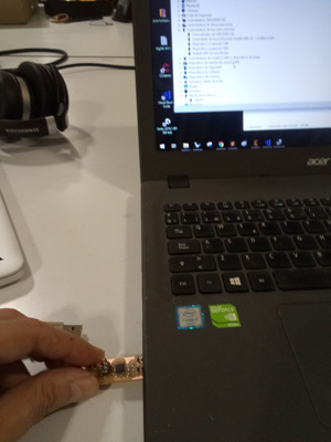
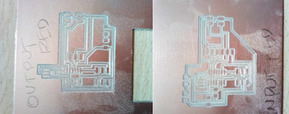
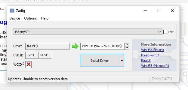
update deburr sharp and jagged copper traces.
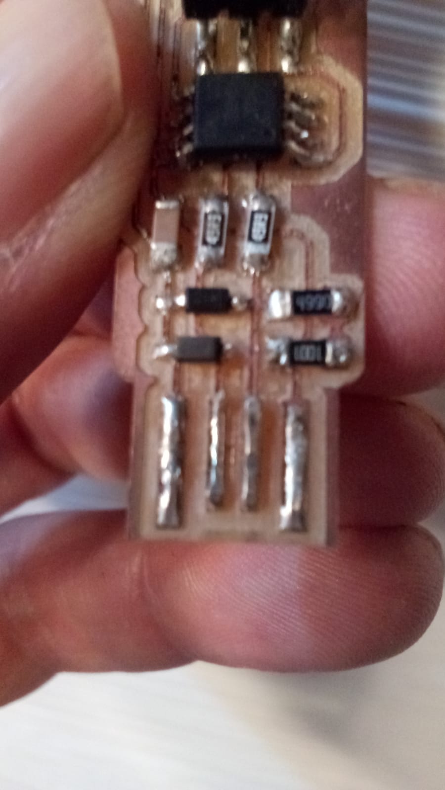
although at the time I did not realize it later during the welding process I proceeded to the smooth sanding of the lines and the removal of the small copper plate from the USB connection
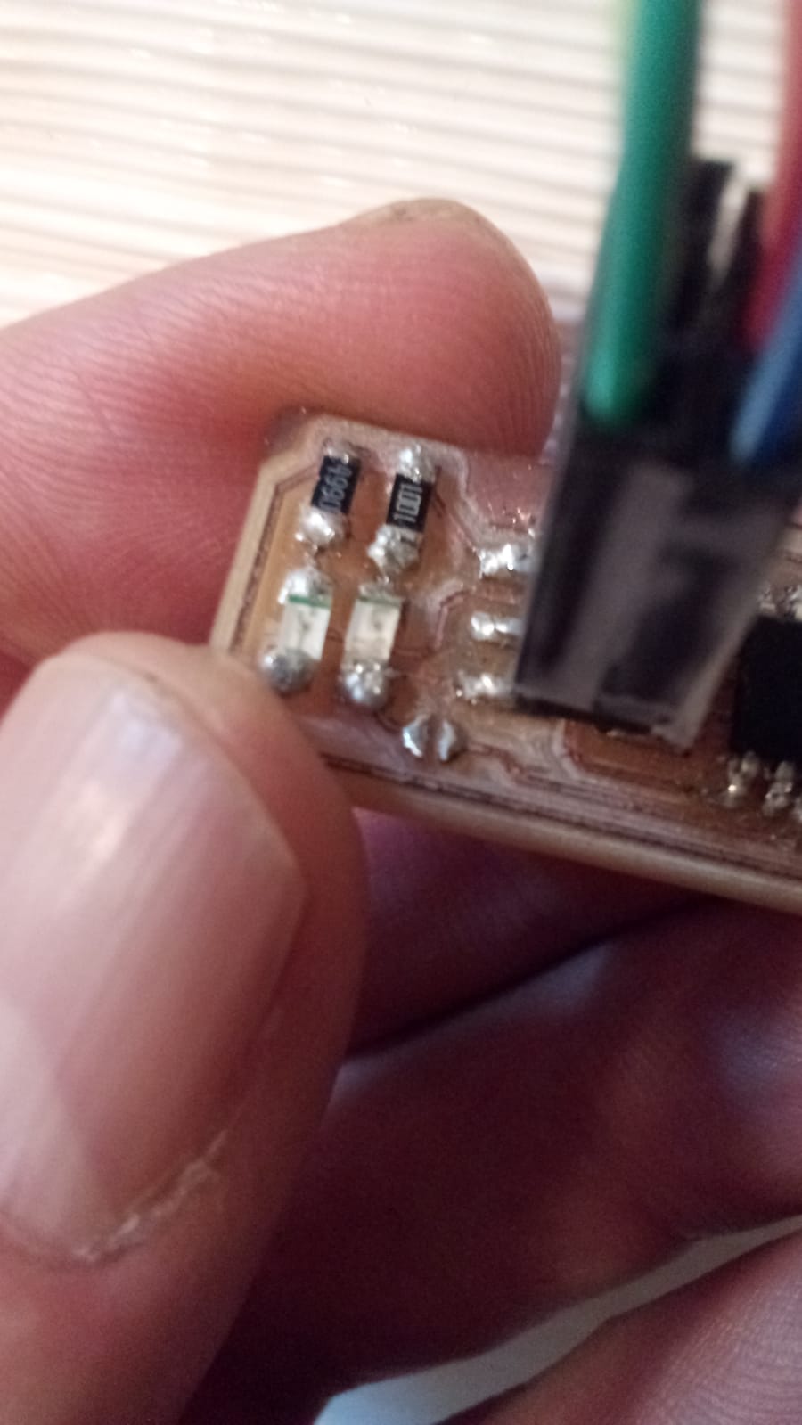
update broken bridge
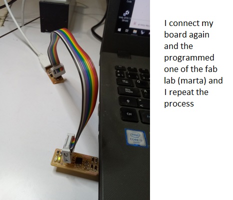
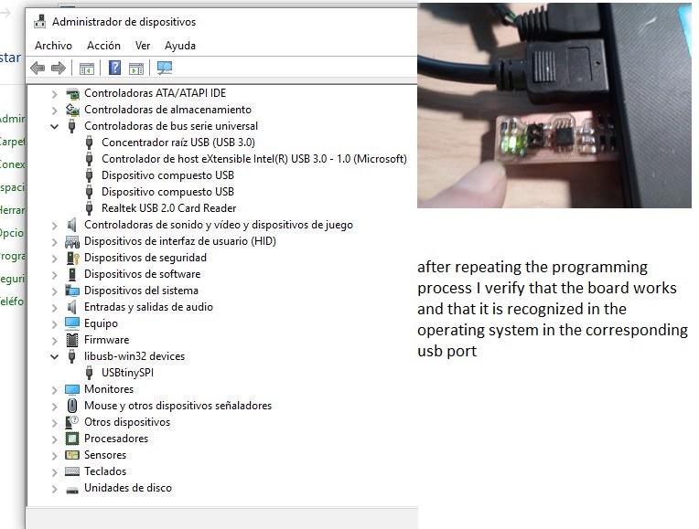
please go for a complete process to the next assignments
if you find some documentation failures in the board manufacturing process please go for a complete process to the assignment 11 "output new board"
//see complete process input board
//see complete process output board
//see complete process network boards