#Week 11 / Input Devices
Assignment and learning outcomes.
What is this week assignment?
For the individual assignment , we must measure something with the sensor it could be for example
We must add this sensor to a microcontroller board that we designed and read information from the sensor using FTDI cable. As a group assignment, we must measure the analog levels and digital signals in an input device using an oscilloscope.
What I gonna do this week?
For this week I what to make a multifunctional board which has more than one sensor. It will have switch buttons and with this switch buttons, I can change from one sensor to another. And also I what to add a push button, with this push button I gonna change the program for one sensor to the program for the other sensor, and probably it gonna have LED for recognizing the changes. I will use the attiny45 microcontroller.
How I gonna do this week assignment?
First I need to decide which sensors I will include on my board, also which microcontroller is good. For understanding which microcontroller I need, I must read the datasheet which I learned from Week 7 Electronics Design(I will try to use Attiny45V-10SU ). After choosing microcontroller and sensors, I need to draw schematics and layout design which I learned from Week 7 Electronics Design. After designing I must manufacture and solder it, manufacturing and soldering skills I learned from week 5 Electronics Production. After manufacturing and soldering, I must program the board, which I learned from week 9 Embedded Programming .
What is the learning outcomes for this week?
The learning outcomes for this week is demonstrating workflows used in circuit board design and fabrication and also implement and interpret programming protocols. And also it is important for documentation to describe your design and fabrication process using words/images/screenshots or link to previous examples, explained the programming process/es you used and how the microcontroller datasheet helped you, explained problems and how you fixed them, Included original design files and code.
Which tools and materials I will use for this week?
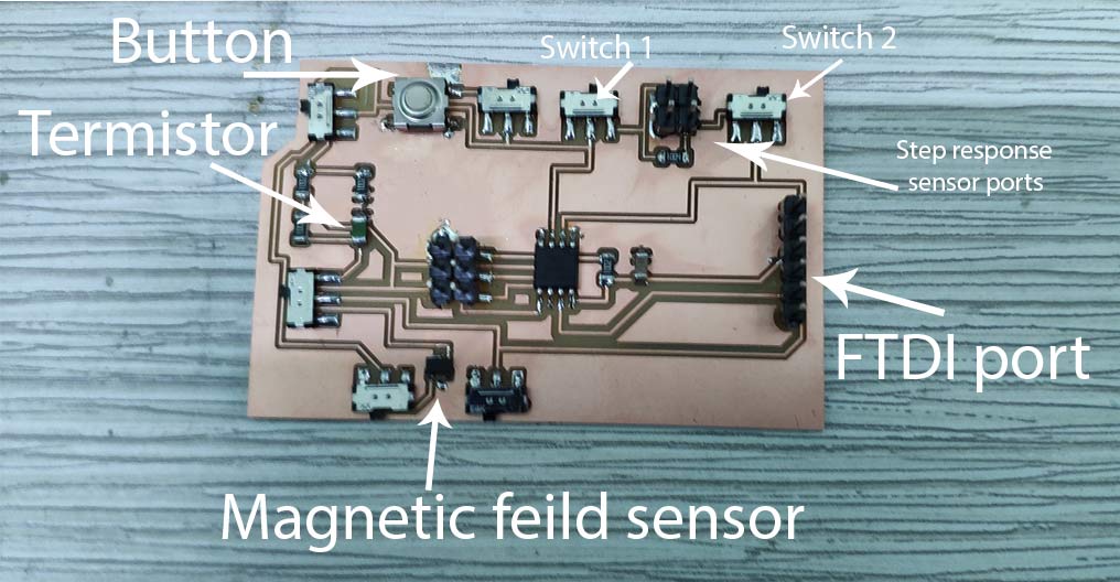
For this week I gonna use KiCad for schematics and layout design, for PCB manufacturing I am gonna use Rolland SRM-20 milling machine, also I gonna use switch, temperature sensor, magnetic field sensor, the step response sensor. I will use attiny45 as a microcontroller.
Which step am I gonna follow?
Individual assignment
Description of step )
In this step, I design the actual board by choosing my board functions and components.
First of all, you need to decide which components you will use(make sure you have all components), after making sure you have got everything the next step is drawing the schematics and layout of your board. After designing and double checking the board design, the next step is milling the board and soldering, and finally program and check if the board is working properly.
Components
My board is multifunctional sensor board so it has 4 sensors, for that, I need 7 switches to switch between them. Components list and their definitions
Schematics
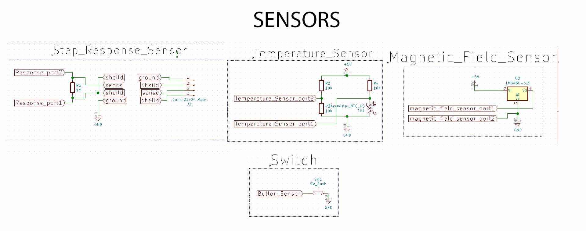
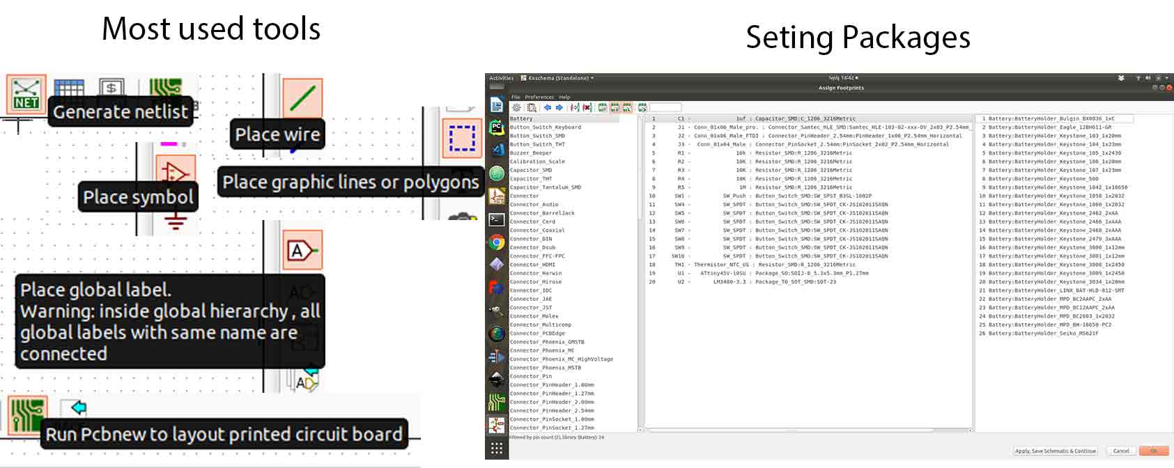
For Schematics and layout design, I used KiCad PCB designing tool. I drow my schematics like block diagram, each block has its label, definitions, and function, and they are connected by “Place global label” function (you can find the icon on the right corner of the panel), it makes schematics more intuitive and understandable for investigation. It consists of 6 main blocks
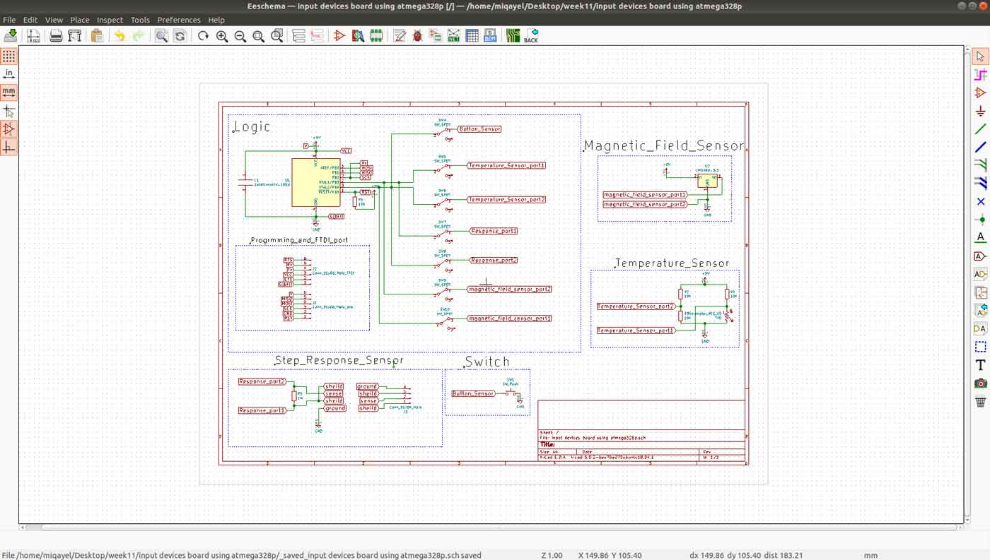
Before making blocks you need to add all components and give them value and number after that connect them (as board sample I used Neils boards). Connections are very simple all sensors I connect to PB4 and PB4 ports through switches, also as general I connect programming connector and FTDI connector to microcontroller pins. Pin connections
After checking all symbols, values, numbers, and connection between parts you can assign footprints for each part (choosing package) by going to “Tools > Assing Footprints”, after choosing a package for each component press “Apply, Save Schematics and Continue”.After click “Generate netlist” by clicking the icon on the top of the panel and finally you have done with schematics. You can go and start work on PCB layout if any problem appears you can go back to change and generate netlist again. If you what to know more how to draw schematics and reading datasheet go to week 7 “Electronics Design”.
PCB layout design
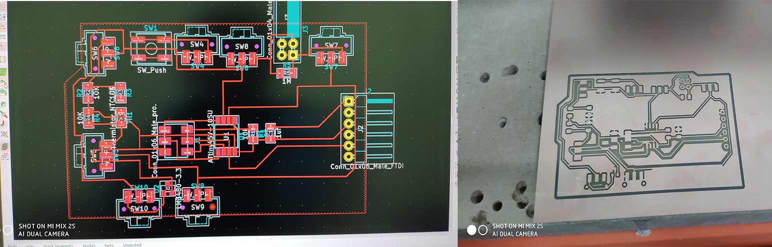
To start layout design you need to click to “Run Pcbnew to layout printed circuit board” icon on the top of the panel. After the program opens the next step is to read netlist that you have generated in schematics program. To add all footprint for all components, you need to click “Read Netlist” icon on the top of the panel and click “Read Current Netlist”, and you will get all footprints. From this point, PCB layout design is started. First, you need to organize all the components optimally. In my case, I tried to use only one layer of the board but I have got a problem with the ground connection. I have solved it by connecting several jumpers in the process of soldering (It is not represented on layout design). After organizing all components (you can do it as blocks like in schematics) next step is connecting them together by choosing “Route tracks” function icon on the right side of the panel. Also, you need to set tracks thickness and Grid to avoid mistakes. In the process of milling your board, you can adjust grid on the upper side of the panel(I have chouse 10.00 mils (0.2540mm) it is not the same diameter as my tool (1/64 inch ) by it is ok ). After setting up the “Grid” next step is connecting components together. Couple advises for connecting
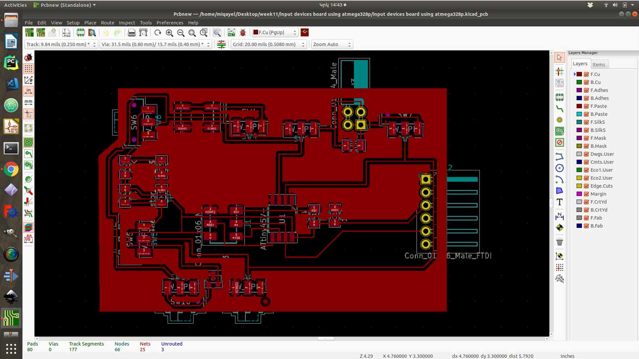
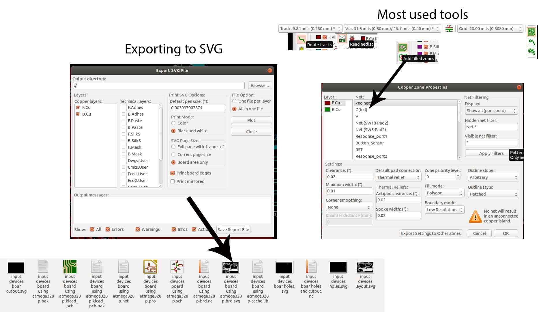
After connecting, the final step before exporting is to “Add Fill Zone ” by clicking the icon in the right corner of the panel and by choosing G(bkl), sketch outline and ground copper(at the same time it will do). And finally, you can export your board in .svg file format by going “File > Export > SVG…>(before clicking “Plot” .Print mode: choose Black and white, SVG Page size: Board area only, ) Plot ” it will save in the project folder.
Board Milling and Soldering
Before milling the board I need to generate g codes for traces, holes and cut out. I have generated all g code by using fab modules web version (for more information on how to use fab modules go to week 5 “Electronics production”). For milling the board I used “Roland SRM-20” milling machine, 1/64, 1/32 inch end mills.
For Information on how to solder the boards go to week 5 “Electronics Production”(the main difference is that I used 3 jumpers to connect all grounds area). Also, make sure that there is no short circuit on the board by using a multimeter.

Programming
For programming, I used Neils Code and FabISP as a programmer. For reading the information I used FTDI cable. Before running the code make sure that you have installed “AVR dude”, connected FTDI cable to the board and the computer.You can check connection by writing on the teminalusb /dev and you should find ttyUSB0(it means your FTDI cable is connected to the computer).

Also, make sure that you have python serial installed (you can check by writing sudo apt install python-serial). After writing lsusb command and check if you're FabISP is connected to your computer check all connections , download .make .c(c code file) and .py(python desktop program ) files from week11( save the link in some folder).

The next step is to run make file by writing make -f hello.button.45.make program-usbtiny it will program your board after run .hex file by writing avrdude -p t45 -P usb -c usbtiny -U flash:w:hello.button.45.c.hex and finally run your python program by writing sudo python term.py /dev/ttyUSB0 9600 (but before check which name your FTDI cable has by writing ls /dev). With the help of the python program, you will get all information from your board. In my case, I need to program each time if I what to use a certain sensor on my board. Here I have only push button code but it will work for any other program, just download files from the site and run it.
This API provides high-level building blocks to communicate with FTDI MultiProtocol Synchronous Serial Engine based on D2XX and FT4222H drivers. The API enables users to write applications and communicate with the FTDI Chip’s I2C/SPI/JTAG/GPIO devices without needing to understand the low-level D2XX and FT4222 drivers and theirs command sets. MPSSE provides a flexible means of interfacing synchronous serial devices to a USB port. Being “Multi-Protocol”, the MPSSE allows communication with many different types of synchronous devices; the most popular are SPI and I2C. Data formatting and clock synchronization can be configured in a variety of ways to satisfy almost any requirement. In addition to the serial data pins, additional GPIO signals are available. The API support Windows and NI Linux RT. The Linux version of LibFT4222 has D2XX built-in.
Conclusion and issues
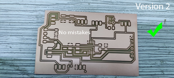
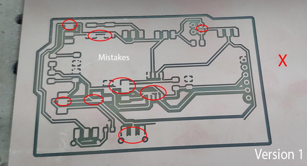
This week was a very interesting week, I have designed my board and make it work as I want. I have also learned how to program the board using terminal commands. I have got some problem regarding the PCB ground. Because I what to make it one layer board, but I find a solution by adding jumpers to connect ground everywhere. Also, I have problems with opening python programs. Button program works well but others are not, in any case, the button program receives the signal from the board. It means the board works good, the only problem is that my computer was not opening other python programs, but I will solve it.