#Week 05 / Electronics Production
Assignment and learning outcomes.
What is this week assignment?
As a group assignment we must characterize the design rules for your PCB production process, and as a individual assignment I need to make an in-circuit programmer by
What I gonna do this week?
In this week I what to make FabTinyISP and program it with AVR programmer “AVRISP mkII”. And after programming the first bord, I what to build a couple of FabTinyISPs and program them with my first programmed FabTinyISP.
How I gonna do this week assignment?
First of all, I need to mill my board on “Roland SRM-20” milling machine, for that I need to generate .nc(g code) or .yml file format in fab modules. For generating files I need an image of traces and outline cutout of the board in .png or .svg file format. Before milling the board I need to make sure that I have all the components for soldering. After milling the board I will solder the board. After soldering I will program it using “avrdude” program and try to program other ISPs with my FabTinyISP.
What is the learning outcomes for this week?
Learning outcomes for the week is to be able to
and also demonstrate correct workflows and identify areas for improvement if required.Also, it is required to show how we made and programmed the board, explain any problems and how we fixed them, and include a “hero shot” of your board.
Which tools and materials I will use for this week?
For this week assignment I will use
Which steps I am gonna follow?
The first step is creating fils for milling, second is mill actual board, third step solder it, fourth step program it.
Step 1) Generating files .
At first I chose the program which can generate files for PCB milling . So I chose Fab modules which is perfect for exporting files for SRM-20 . Also there is desktop version which you can download on your computer but I used the web version which is very easy to use .
Step 1.1) Go to http://kokompe.cba.mit.edu/ .Step 1.2) Go to current: http://fabmodules.org/ .
Step 1.3) Choose the image format and import it on website .The available formats.
- .png
- .svg
- .stl
- .vol
- I download FabISP layout and cutout images from here .
- Also you can design your own PCB and export it in .png format .
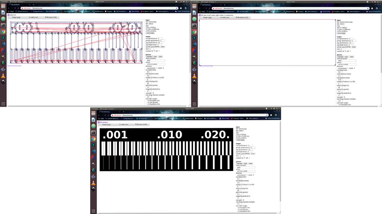
Step 1.5) Choose export format of the file . This is important because it must be readable for your machine . In my case I chose G-Code format which is working with different kinds of machines including SRM- 20 .There is also .rml file format which is exactly for SRM-20 and MDX-40 . But I used .nc or in another words G-code format in any case if your machine is different of mine .
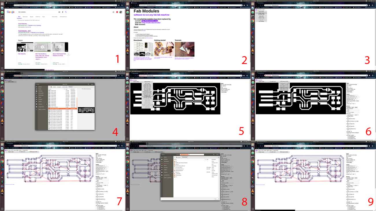
Step 1.6) Choose 1/64 inch tool for traces .
Step 1.7) Adjust the parameters .
- cut depth
- tool diameter
- number of offsets
- offset overlap
- path error
- image threshold
In my case I haven't changed anything , I calculated it by default parameters . So after looking through parameters press calculate and wait .
Step 1.8) Press “Save” and save somewhere .
Step 1.9) Restart the page choose outline image and choose 1/32 inch tool for it (the file format is the same .nc ) . You can change the parameters , but I prefer to save it by default . And after saving the you got 2 files one for layout and one for cutout .
Step 2) Preparing for Cut .
Step 2.1) Clean up the area of machine , and board (make sure there is no oil on it).
Step 2.2) Make shure you got all tools
- Double side tape .
- Milling bit 1/64 .
- Milling bit 1/32
- Cuter for paper .
- Vacuum cleaner .
Step 2.3) Stick Double-sided tape on the board tightly .
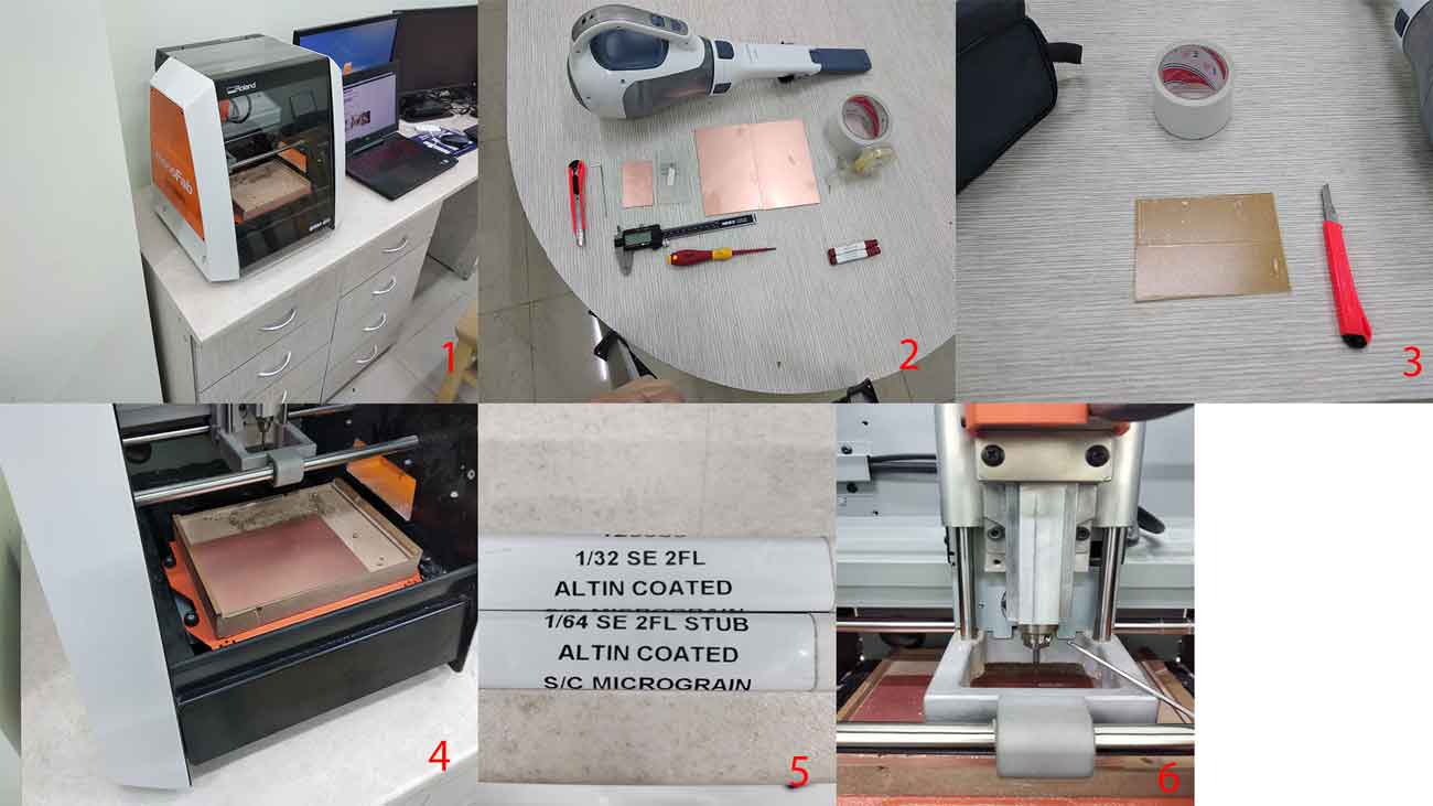
Step 2.4) mount board inside the machine . ,
Step 2.5) Choose tool .
- For layout 1/64 inch .
- For cutout and holes 1/34 inch .
Step 2.6) Tight the tool in the spindle (By holding with the finger)
Step 3) Setting up the Roland SRM-20 with Vpanel - X,Y,Z Zero , Importing files , cut out .
Before starting these steps you must read the manual .
Step 3.1) Open Vpanel for SRM-20 .
Step 3.2) Choose G54 in “Set Origin Point ” on the right side .
Step 3.3) Choose G54 in the left side .
Step 3.4) Go to Setup and choose “RML-1/NC Code ”
Step 3.5) Choose the tool , at first 1/64 inches . (If you have not done it yet )
Step 3.6) Tight the tool in the spindle.(If you have not done it yet )
Step 3.7)Move the tool wherever you what to zero it .
- You can move it by using buttons in the middle +Y , -Y , +X , -X , +Z, -Z(be carefully with Z), you can adjust the speed of movement in “Cursor Step ” section .
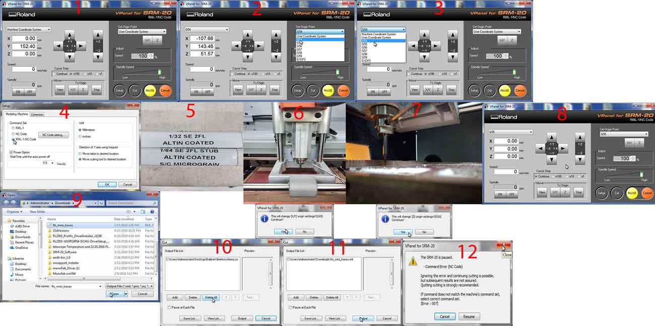
Step 3.8) Press “X/Y” on the right side and click “Yes” , and press “Z” “Yes ” , it will change the origins by 0 .
Step 3.9)Make sure you have generated the files in Step 1 .
Step 3.10)Click “Cut” and press “Delete All”
Step 3.11)Press add button and choose the g-code file . At first 1/64 inches file and press output .
Step 3.12)Press “Red X ” , and the machine will start the milling proces .
Step 3.13)When it finish , press “View” button in the “Move” section .
Step 3.14) Change the tool to 1/32 inches .
Step 3.15 ) Zero the Z origin .
Step 3.16) Output the cut out file .
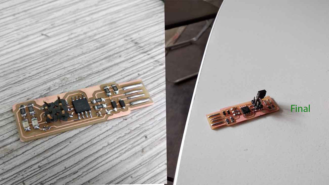
And finaly will get the board .
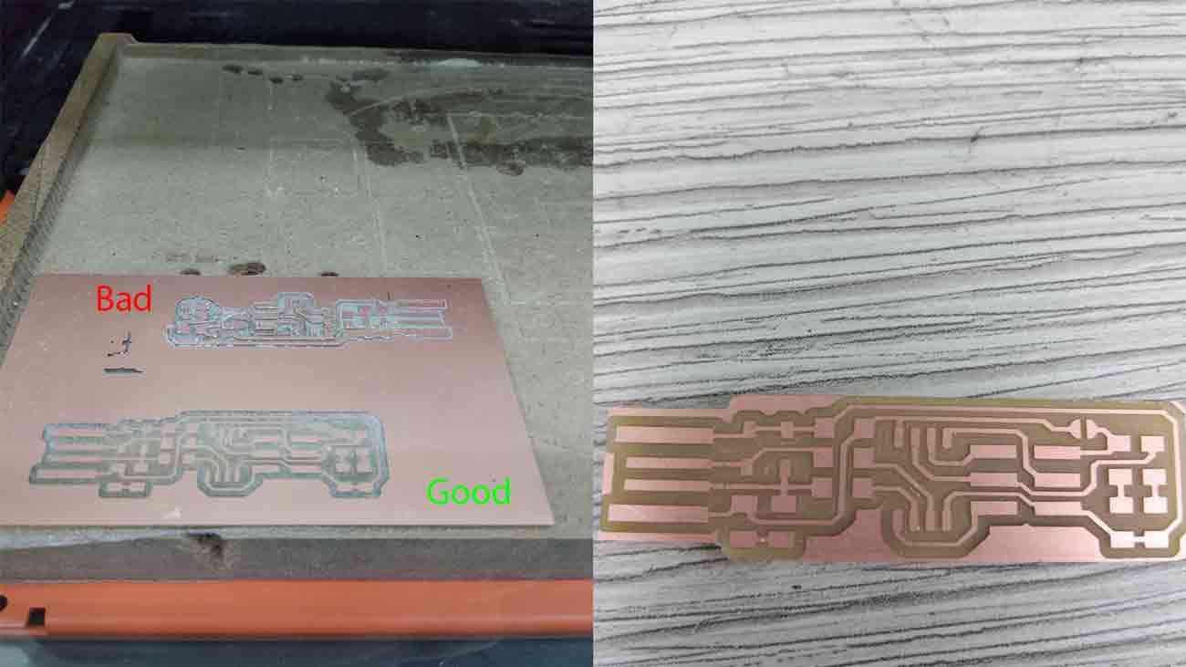
The same process we have done on group project , and got this .
.jpg)
Step 4) Soldering
Step 4.1) Clean up the space around .
Step 4.2) Make sure you have .
- Soldering Iron.
- Cuter .
- Fume Extractor for Soldering
- Solder Wire
- Flux
- Soldering sponge
- Pinset
Step 4.3) Make sure you have the electrical components .
- ATTiny45 -1x
- 49.9 ohm resistor - 49R9 - 2x
- 1k resistor – 1001- 2x
- 499 ohm resistor – 4990 -2x
- 3.3V Zener diode – 2x
- Red LED -1x
- Green LED -1x
- 100uf Capacitor -2x
- 2 pin header -3x
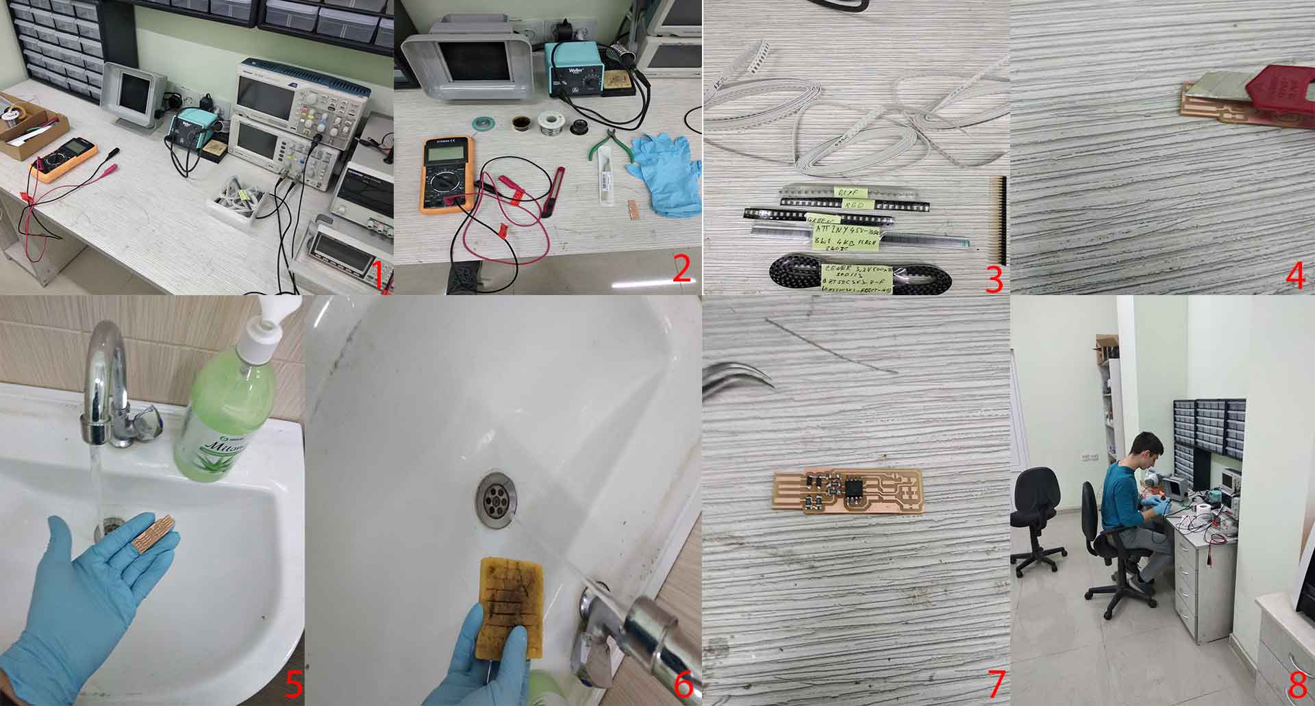
Step 4.4) Remove unnecessary parts on the board with cutter .
Step 4.5) Clean up your PCB with water .
Step 4.6) Water the soldering iron sponge .
Step 4.7) Start Soldering
- Make sure that soldering iron is about 350 degree celsius .
- Make sure that ventilation is working well (because the smoke is dangerous if you breathe a lot )
- Clean the parts to be joined
- Clean soldering iron tip and "tin" all faces of tip with a coating of solder
- Heat parts ,not solder, to be joined
- Apply flux-core solder to heated parts, not the soldering tip, and heat it till solder melts and flows freely
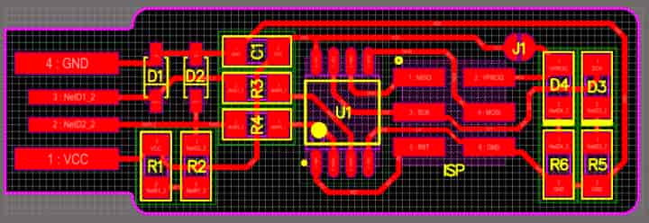
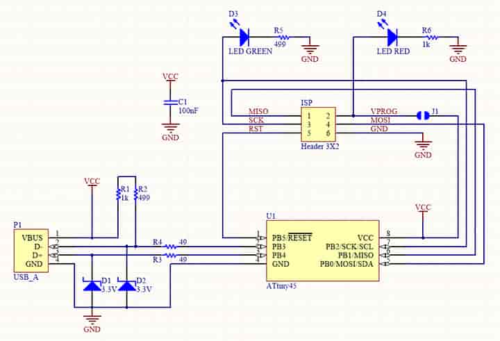
Step 4.8) Solder by looking on schematics and layout .I added a jumper , after programming you can put it in one pin .
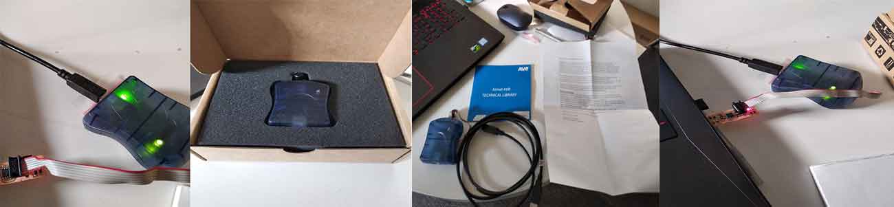
Step 5)Programming
Connect AVR programmer to computer , connect your board to computer , and connect AVR to your board .
Step 5.1)Open terminal and write these command
sudo apt install avrdude gcc-avr avr-libc make
Step 5.2) Downloaded Firmware source code files from here .
Step 5.3) Extract Firmware files .
Step5.4) cd to that folder and write
make
command(this will produce .hex file which will be programmed into ATtiny 45.)
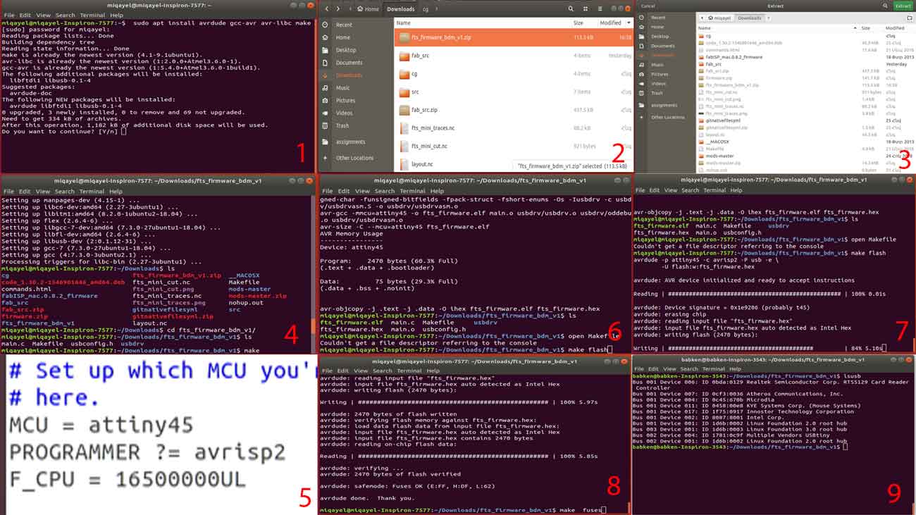
Step 5.5)Next is update makefile with USB name, for this, run gedit in terminal, open makefile in your firmware folder, edit the name usbtiny to avrisp2. And save the file.
Step 5.6) run command make flash(it will program the ATtiny45 memory ) .
Step 5.7) run makefuses .
Step 5.8)Remove AVR and Attiny board , and plug in Attiny board again .
Step 5.9) Run lsusb comman , it must show .Bus 001 Device 009: ID 1781:0c9f Multiple Vendors USBtiny
Step 5.10) Program other boards with your programmer , in the same way .
.jpg)
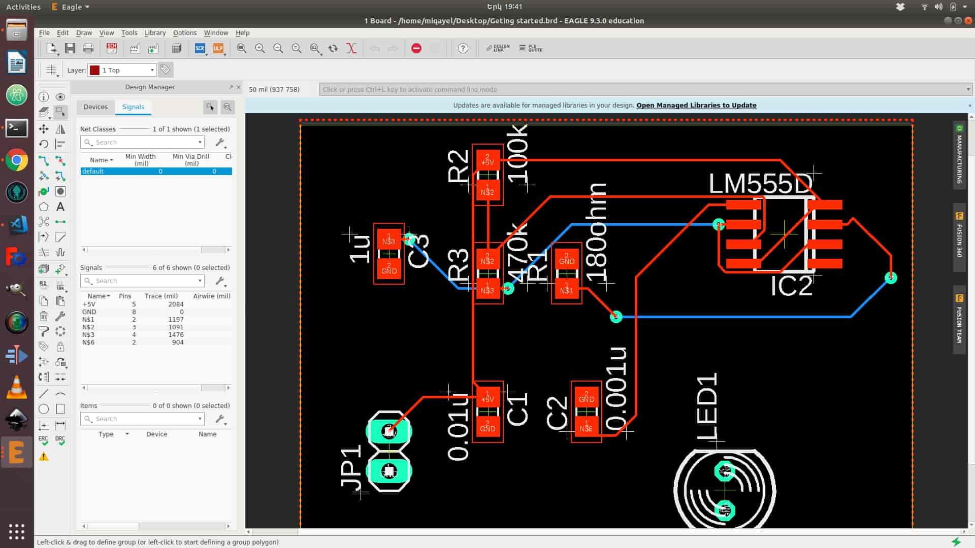
Step 6) Designing my own borad
For Circuit Designing I chose Autodesk eagle .You can download it on linux free for 3 years , also available for Windows and MacOS .
Step 6.1)Create Project
Step 6.2)Create schematics
Step 6.3)Add components
Step 6.4)Add Connect them together
Step 6.5)Write values
Step 6.6)Open layout
Step 6.7)Arrange the components
Step 6.8)Connect them
Step 6.9)Export as gerber or .png image formats .
In this images I just try out the software , for learning purposes .
.jpg)