Reading a Datasheet
What is Datsheet?
From this video I leraned How to reverse engineer and read a datasheet For our purpose
It's a detailed document describing all the features about a specific product similarly in electronics like microcontrollers and sensors it's adviced to read a Datsheet and proceed because that gives a full idea about how the product is going to work in certain environment,
say how a sensor will behave in extreme weather conditions, or a microcontroller will work at a particular volatage or current, it contains the controller's detailed architecture etc...
Personally reading a 200-250 page documentation is kind of boring and but let's not be naive about it and get started..
AT TINY 44
So I found two Datasheet on the internet one from the official link of MicroChip and One from MIT lab they were literally same just the MIT one has more number of pages I haven't read the all datasheet I just went throug the setions that were required and coulb be understood my lil mind.
Datasheet Official Microchip -194pgs
Datasheet MIT fablab link- 229pgs
Altough they both are the same
I didn't get all of them, I watced it thrice, but somehow I got to know what to search and how to search particular things in a datsheet.
Here's the keypoints from the data sheet-
						    >Program Memory Type      : Flash
						    >Program Memory           : 4KB
						    >CPU Speed                : 20 MIPS
						    >RAM Bytes                : 256
						    >DATA EEPROM Bytes        : 256
						    >Digital Communication    : 1SPI , 1 I2C
						    >Capture/ Compare / PWM Peripherals : 1 Input Capture, 1CCP, 4 PWM
						    >Timers                   : 1 x 8bit, 1 x 16bit
						    >Comparators              : 1
						    >Temperature Range        : -40 to 85
						    >Operating Voltage        : 1.8 to 5.5V
						    >Pin Count                : 14
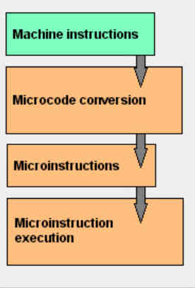
It's a low power AVR 8 bit Microcontroller based on Advanced RISC architecture.
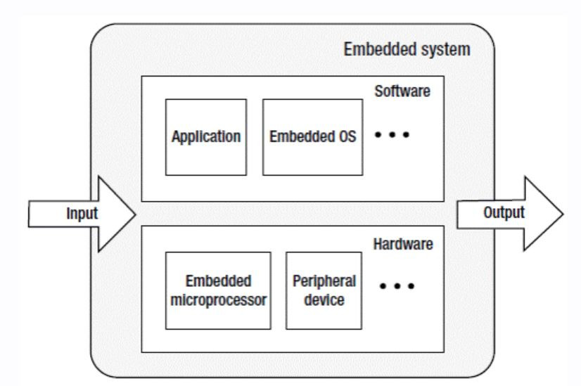
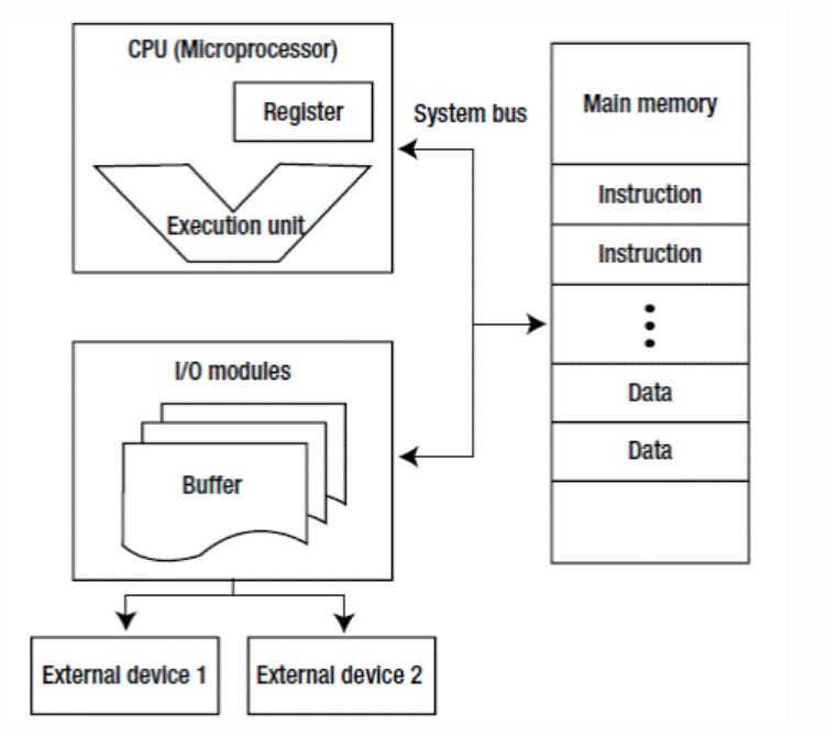
What is meant by architechture?
Computer architecture is a set of rules and methods that describe the functionality, organization, and implementation of computer systems. Some definitions of architecture define it as describing the capabilities and programming model of a computer but not a particular implementation. In other definitions computer architecture involves instruction set architecture design, microarchitecture design, logic design, and implementation.
~Wikipedia
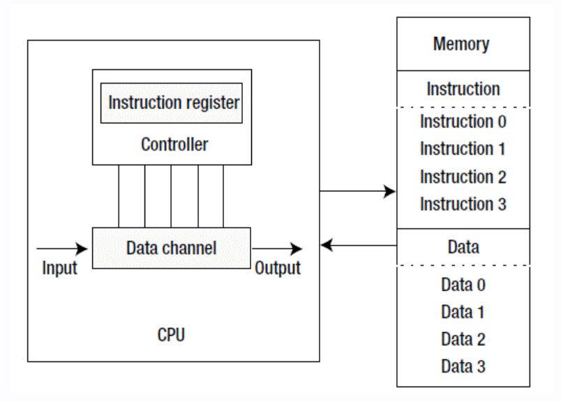
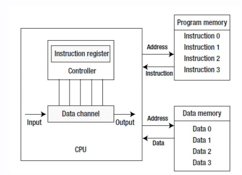
Understanding RISC and CISC
RISC
CISC
The term RISC stands for ‘’Reduced Instruction Set Computer’’. It is a CPU design plan based on simple orders and acts fast.
The term CISC stands for ‘’Complex Instruction Set Computer’’. It is a CPU design plan based on single commands, which are skilled in executing multi-step operations.
This is small or reduced set of instructions. Here, every instruction is expected to attain very small jobs. In this machine, the instruction sets are modest and simple, which help in comprising more complex commands. Each instruction is of the similar length; these are wound together to get compound tasks done in a single operation. Most commands are completed in one machine cycle. This pipelining is a crucial technique used to speed up RISC machines.
CISC computers have small programs. It has a huge number of compound instructions, which takes a long time to perform. Here, a single set of instruction is protected in several steps; each instruction set has additional than 300 separate instructions. Maximum instructions are finished in two to ten machine cycles. In CISC, instruction pipelining is not easily implemented.
~ Source
link
The below image shows the very important pinout for the Attiny 44, in order to make sure of the connections and also the placement of the component.
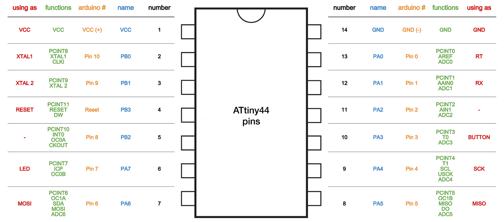
Source ~
link
PIN Descriprions
The content below is mostly from Datasheet I've tried somewhere to explain it in my words.
Supply voltage
Ground
Port B is a 4-bit bi-directional I/O port with internal pull-up resistors (selected for each bit). The Port B output buffers have
symmetrical drive characteristics with both high sink and source capability except PB3, which has the RESET capability.
To
use pin PB3 as an I/O pin instead of RESET pin, program (‘0’) RSTDISBL fuse. As inputs, Port B pins that are externally
pulled low will source current if the pull-up resistors are activated.
The Port B pins are tri-stated when a reset condition
becomes active, even if the clock is not running.
Reset input. A low level on this pin for longer than the minimum pulse length will generate a reset, even if the clock is not
running
Port A is a 8-bit bi-directional I/O port with internal pull-up resistors (selected for each bit). The port A output buffers have
symmetrical drive characteristics with both high sink and source capability. As inputs, Port A pins that are externally pulled
low will source current if the pull-up resistors are activated. The port A pins are tri-stated when a reset condition becomes
active, even if the clock is not running.
Understanding The PULL UP and PULL DOWN Resistances
You can go to my Week 7 where I explained aboutt PULL-UP resister and how to calculate it's value from
here.
Digital logic gates can be used for connection to external circuits or devices but care must be taken to ensure that their inputs or outputs function correctly and provide the expected switching condition.
Modern digital logic gates, IC’s and micro-controllers contain many inputs, called “pins” as well as one or more outputs, and these inputs and outputs need to be correctly set, either HIGH or LOW for the digital circuit to function correctly.
We know that logic gates are the most basic building block of any digital logic circuit and that by using combinations of the three basic gates, the AND gate, the OR gate and NOT gate, we can construct quite complex combinational circuits. But being digital, these circuits can only have one of two logic states, called the logic “0” state or the logic “1” state.
These logic states are represented by two different voltage levels with any voltage below one level regarded as a logic “0”, and any voltage above another level regarded as logic “1”. So for example, if the two voltage levels are 0V and +5V, then the 0V represents a logic “0” and the +5V represents a logic “1”.
If the inputs to a digital logic gate or circuit are not within the range by which it can be sensed as either a logic “0” or a logic “1” input, then the digital circuit may false trigger as the gate or circuit does not recognise the correct input value, as the HIGH may not be high enough or the LOW may not be low enough.
For further info about pullup and pull down I found this amazing article on the web you can refer to that with this
Source link.
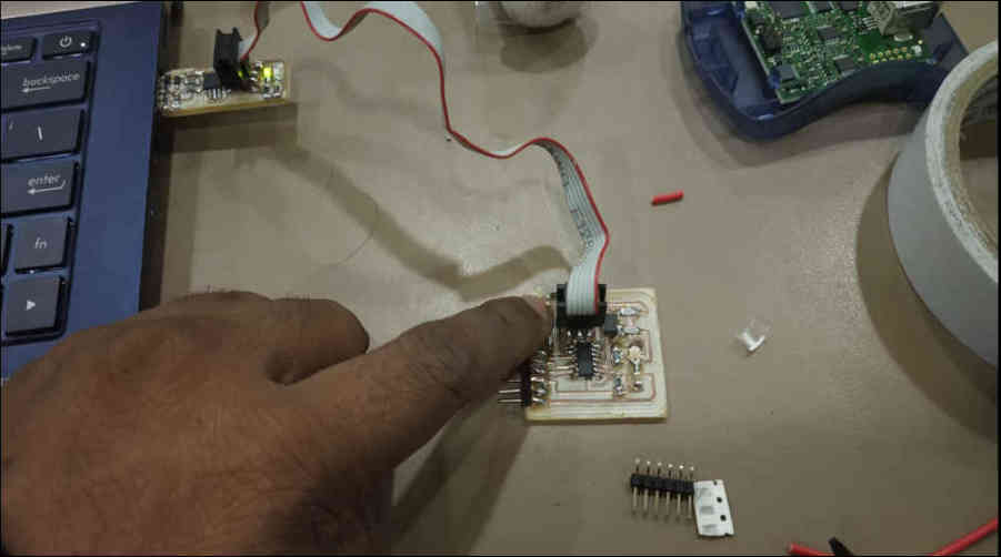
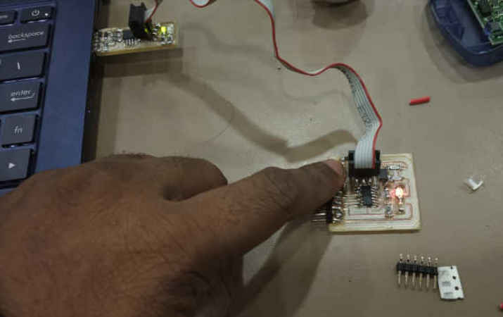
Programming PINs
						SCK(Serial Clock): Programming clock, generated by the In-System Programmer (Master)


						MOSI(Master Out - Slave In ): Communication line from In-System Programmer (Master) to target AVR being programmed (Slave )


						MISO( Master In - Slave Out ): Communication line from target AVR (Slave) to In- System Programmer (Master)


						RST(Reset): To enable In-System Programming, the target AVR Reset must be kept active. To simplify this, the In-System Programmer should control the target AVR Reset


						GND(Ground): Common Ground


						VCC(+5V): +5V input
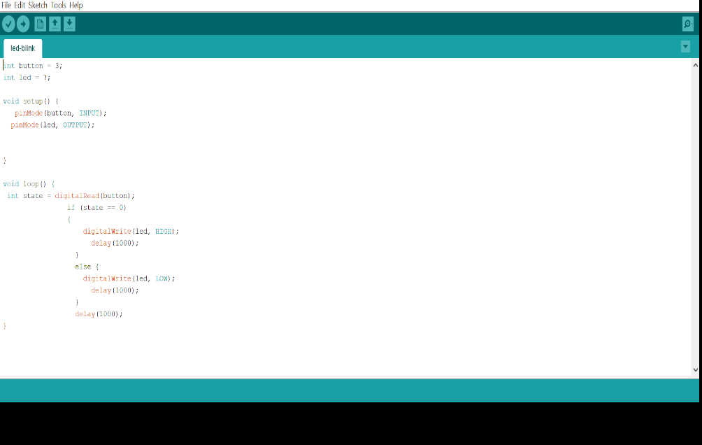
 Not Pressed
 Pressed