Starting Off with Eagle
Eagle is a PCB designing Software which is not fully Open Source but it can download it Under a student Licence and on the very basic ground it doesn't makes an difference all the necessary options, tools are vailabele iin the education licenced version.
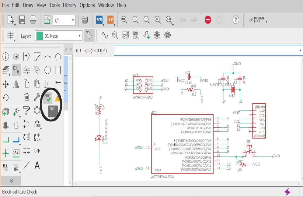
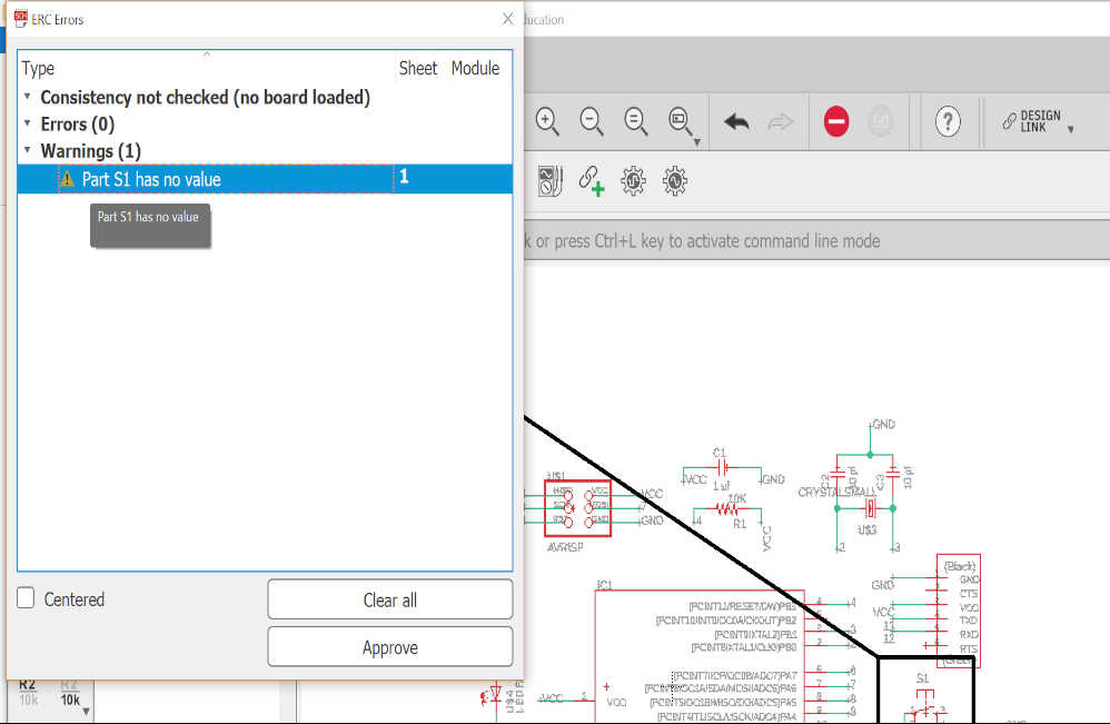
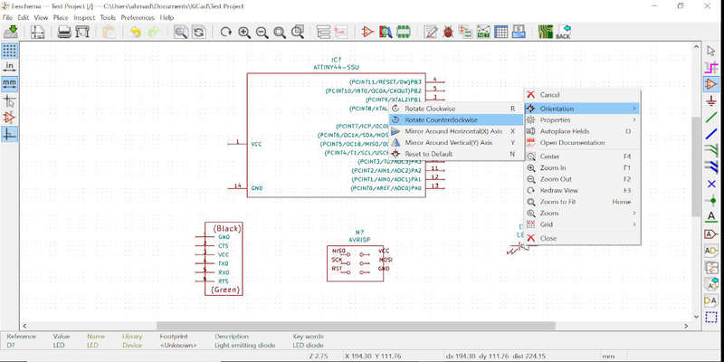
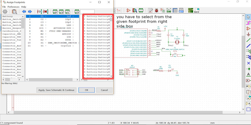
Fortunately I did not get any error just a warning that my switch S1 had no value like I did not assigned any value to it, as it was not rewuired to asssign the value to the pushbutton so that can be ignored.
It is avilable for all type of platform, I use windows ..
I downloaded the latest version of Eagle 9.3.1 from this
link.
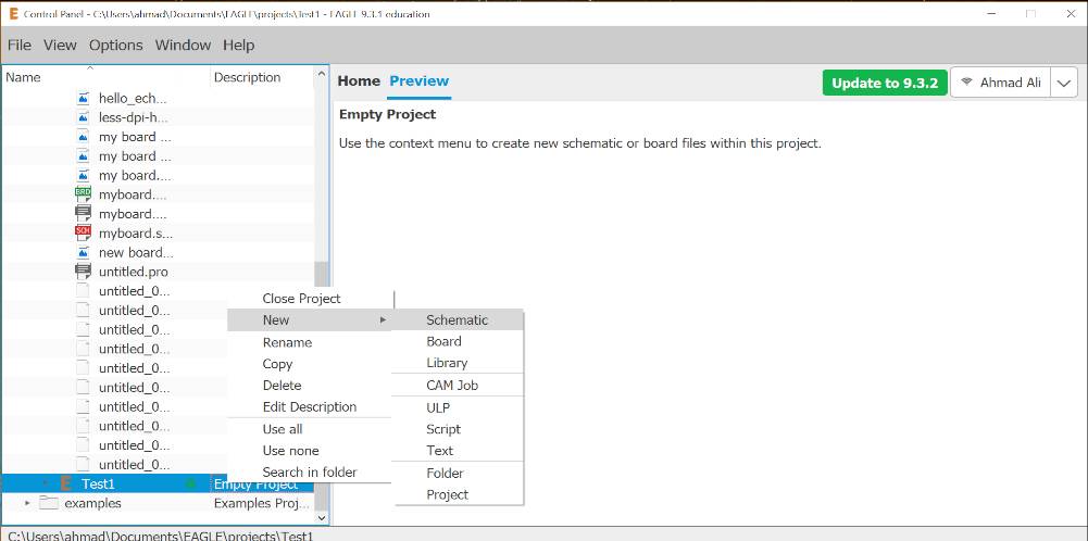
Then I opened a New project on the eagle and give it a name and then click on the project,
There were various options as u can see from the below slider image number 3rd so I need to make a schematic of the board so I selcted schematic and proceeded.
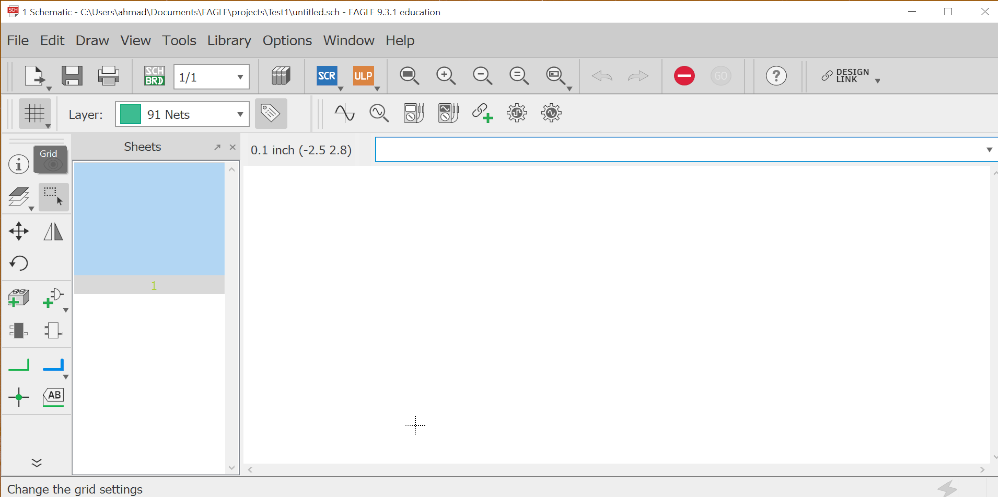
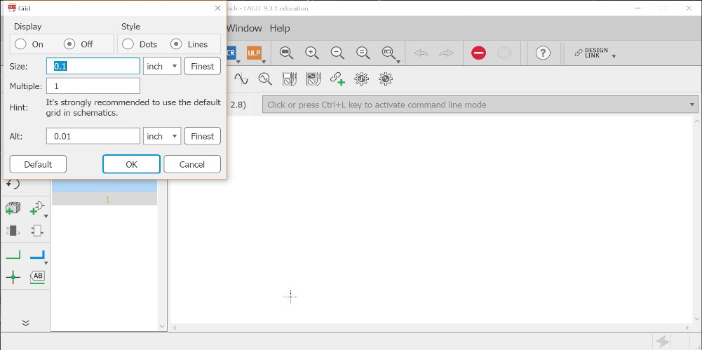
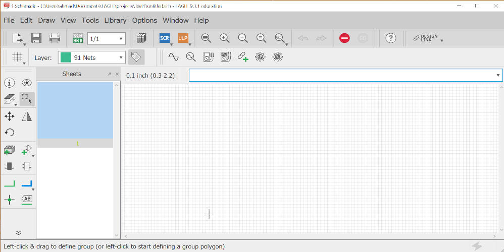
On the top right Icon there sis a grid setting I turn it on for better placing of the components.
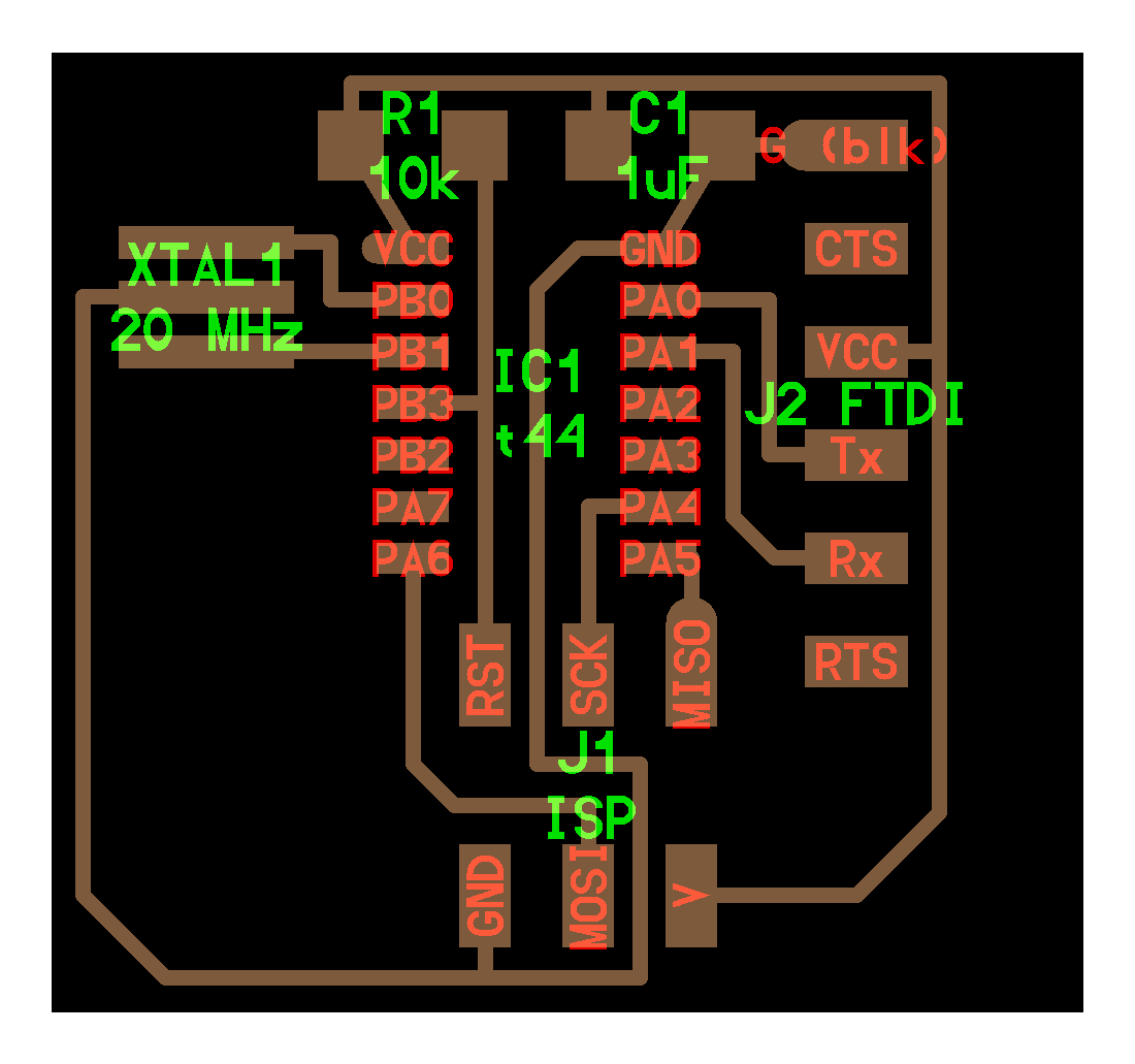
Now let's analyse the circuit that is to be made,
The components used here are-
So, Similar to what we have done in CAD week i.e the designing of the mechanical parts giving them the appropriate dimensions and all,
likewise in PCB designinig too there are various packages, like the same IC of Attiny can be manufactured in many forms like throughole, SMD, etc.
depending on the type of usage and size the person opts for the right package.
Keynote: Selecting the right package of components is very important because it will reflect that in the board layout.
Every component has a footprint which is basically its layout which can be made manually but the easier and best way is to use the libraries.
Libraries contains the files and footprints of the components.
For making the schematic it is necessary to choose the components which is of right package. One can add as many library files in the eagle.
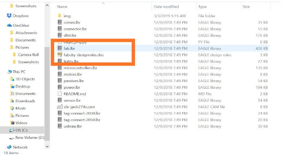
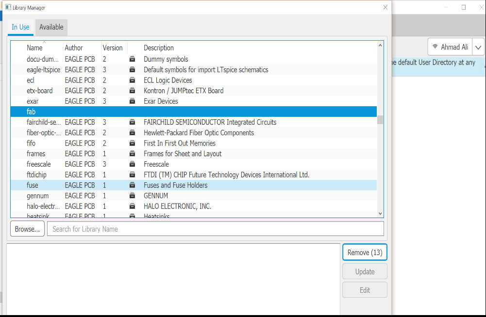
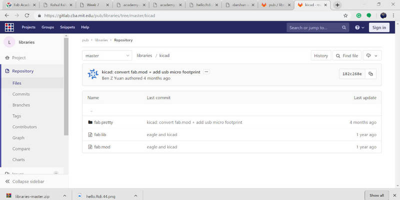
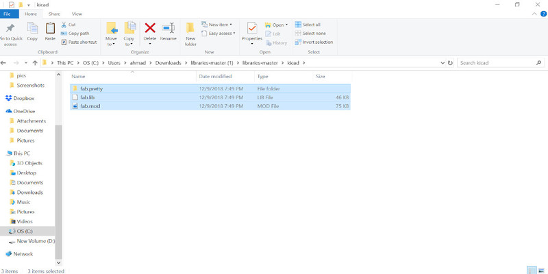
I downloaded the Fab.library from this link which is given on the schedule page of Electronics Design week.
Then I extracted and pasted the .lbr file in the library folder of eagle,
for me it was
-->C-->Eagle 9.3.1 --> eagle
in this folder many other .lbr files were already there so I pasted the fab.lbr in this folder.
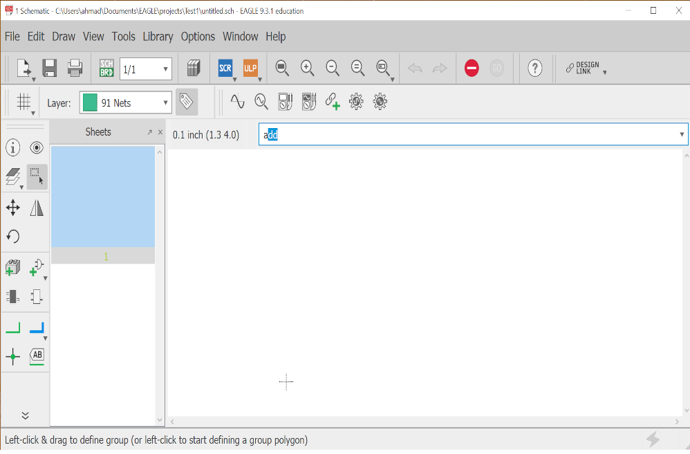
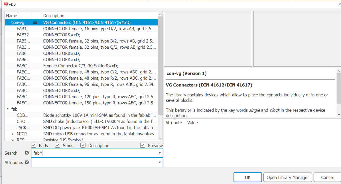
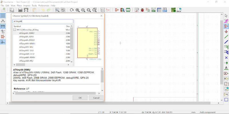
Now it's the time to add the components for the schematic it's pretty easy you just have to type 'add' on the command box and hit -->Enter.
You will be redirected to a list of componrnts i just typed fab*(* to show me the library and components it contains).
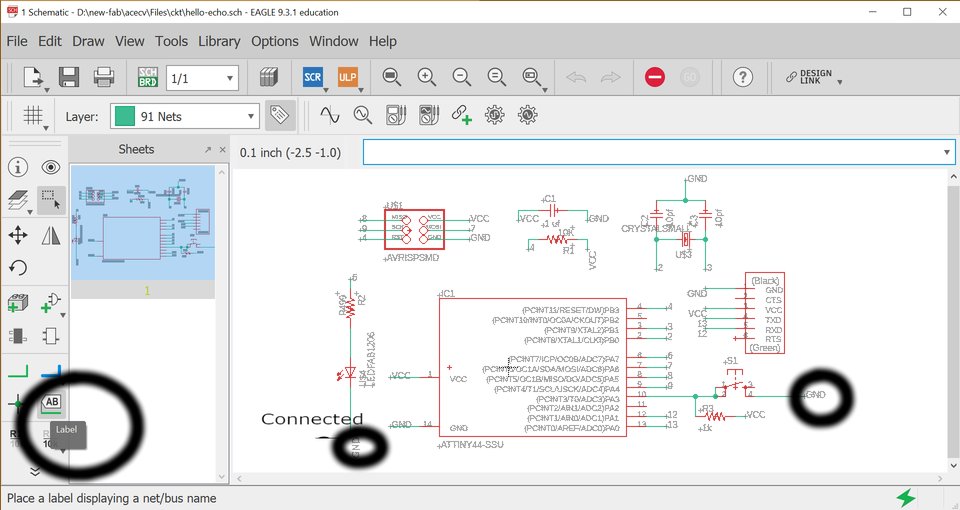
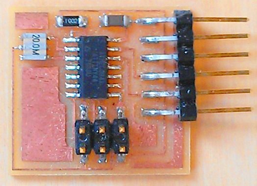
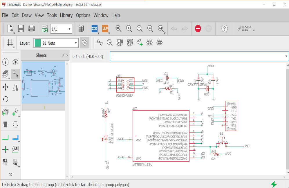
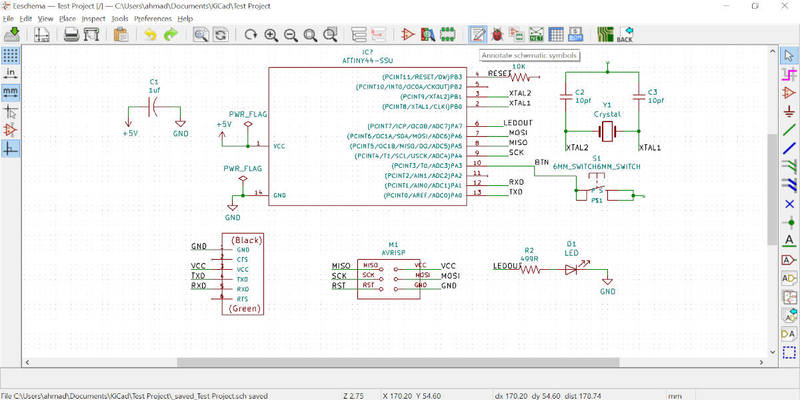
The final Schematic looked like this-
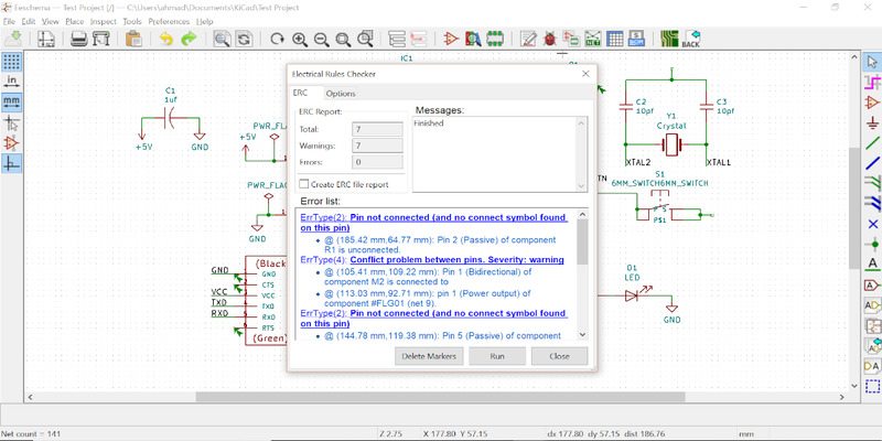
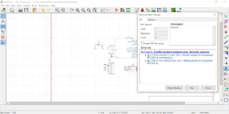
Checking the ERC- Electric Rules Check
This is a handy tool that allows to point out common errors in your schematic. An ERC will check for the following issues:
Types of ERC Errors
When you run an ERC for the first time, you’ll be presented with several error categories, including:
Consistency Errors:
 This error means that something isn’t right between your schematic and PCB layout, and your changes likely aren’t in sync between both files. If you get one of these errors, consider it a major red flag to compare both versions of your design before moving ahead.
Errors:
 Errors are the red stoplights. You need to step on the breaks and check these out before proceeding. Errors can be pretty significant, like having an unconnected pin that will throw your whole circuit out of whack.
Warnings:
 Warnings are the yellow stoplights. While these types of errors might not mess up your design if you move forward without fixing them, it’s good practice to slow down and review them one by one. These guys are minor compared to Errors, and n include many non-design breaking issues like missing net values.
Source-https://www.autodesk.com/products/eagle/blog/schematic-basics-part-3-erc/
Error I got:
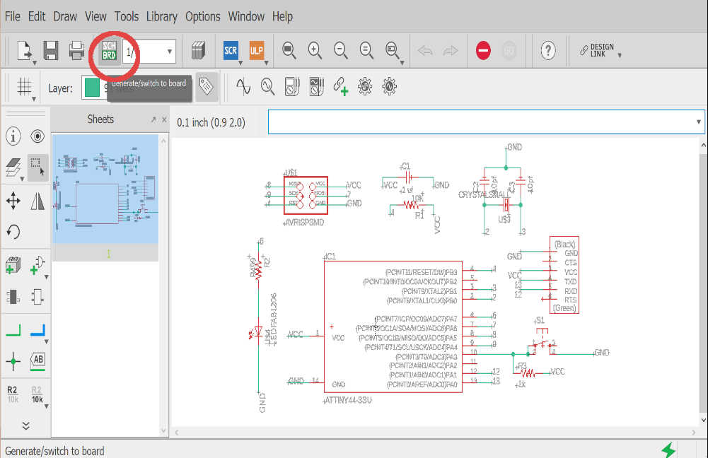
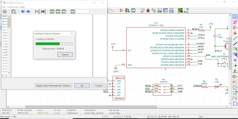
Creating the Board from schematic
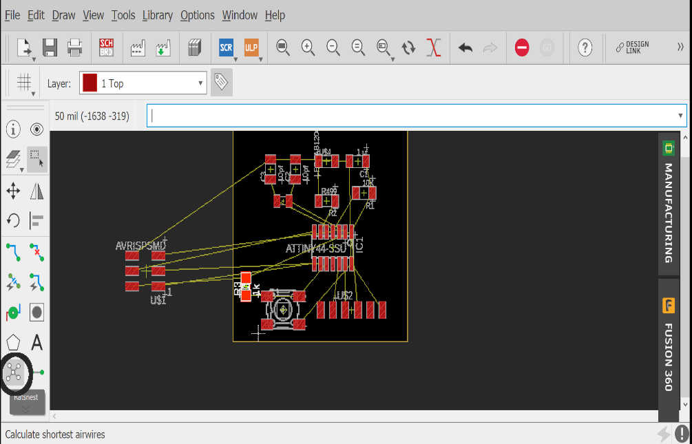
On clicking on the top we Brd/Sch tab We enter into the board view where all the footprints of Schematic are present and I need to manually arrange all the component in a particular layout to solve like a puzzle so when routing my wires don't overlap each other.
In the process of placing the components use the rastnet too just to clear all the excess air wires.
Now u have to create a route or traces of your board which is to be build, it's kinda like solving a jigsaw puzzle but thanks to the Autorouter feature of Eagle. Let's see how i used it..
Need of Resistances and Calculating It's Values
LED's are fragile in terms of amount f current flowing to them, a high current will blow of the LED so a need of current limiter is required in fomr of a resister.
Claculation of the value can be done by using Ohm's Law-
Ohm's Law is given by:
V = I R
where V is the potential difference between two points which include a resistance R.
I is the current flowing through the resistance.
Based on the above formula and the Datasheet of the Red LED which has been used for the accurate information regarding voltage and current, I calculated that if
Voltage (V)is 5 Volts and Current (I) is 20 Miliampere (i.e 0.02 Ampere) so the resistance (R) is the Voltage divided by the current as shown below:
R = V/I
= 5 / 0.02
R = 250 ohm
The calculation as per the formula explains I need at least 250 ohm resistance and so accordingly I select the closest resistor available -499R for the above mentioned function and purpose.
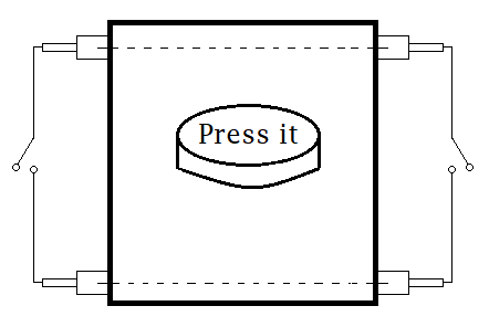
Button
Reference from -
https://circuitdigest.com/electronic-circuits/push-button-led-circuit
Button with the "push-to-make" (normally-open or NO) mechanism are a type of push button electrical switch that operates by the switch making contact with the electronic system when the button is pressed and breaks the current process when the button is released.
I used A pullup resister of 10K to my button.
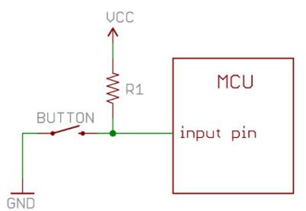
With a pull-up resistor, the input pin will read a high state when the button is not pressed. In other words, a small amount of current is flowing between VCC and the input pin (not to ground), thus the input pin reads close to VCC. When the button is pressed, it connects the input pin directly to ground. The current flows through the resistor to ground, thus the input pin reads a low state. Keep in mind, if the resistor wasn’t there, your button would connect VCC to ground, which is very bad and is also known as a short.
Pull-Down:
Similar to pullup the end is connected to ground so as the button is pressed ground formed or Vcc flows along the ckt.
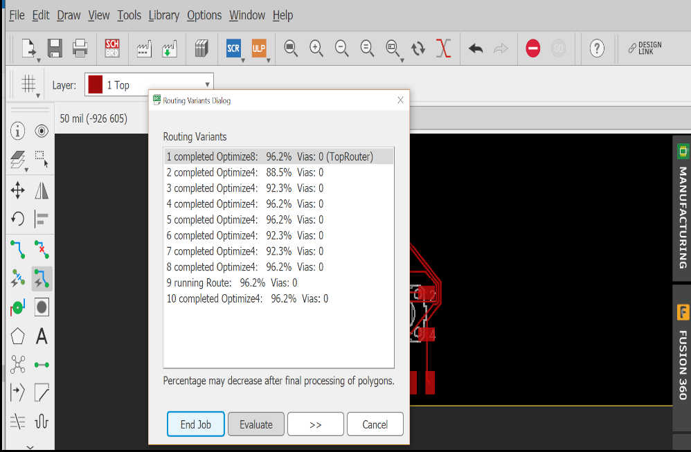
Routing Your Board With the Autorouter
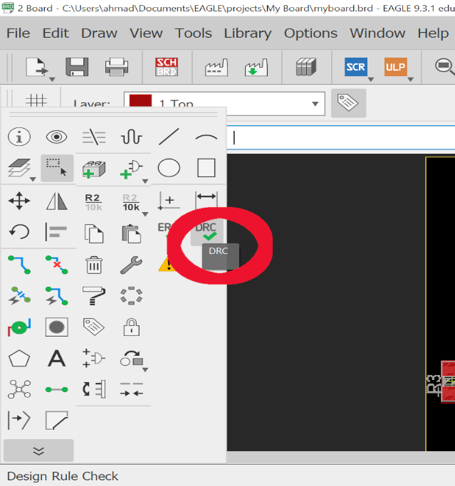
Doing a DRC check Design rules
Reference taken from an article on quora- https://www.quora.com/How-do-I-use-auto-router-on-Eagle-PCB-design
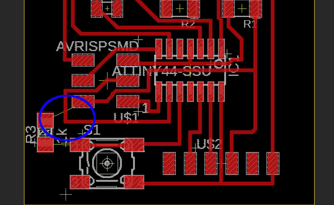
My routing was 94% and there was one air wire from the VCC to the resister of led so I left that planning to add a jumper wire along it.
Say If you are making a circuit where a relay is used or a constant high current is going to be flown on that trace then you need to make that trace bit wider than othre traces where the current is low. here For my design I chose the size to be 16 mils.
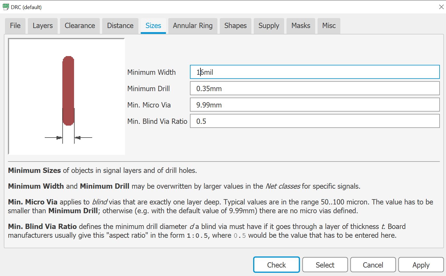
Then click on Clearance and set the following parameters.
Again you only need to set clearance in first column depends of how much clearance you want in your design only I used 14 mils clearance for the design. It's basically the distance between the traces the pads and the traces, After that click on the apply button.
![]()
For my design I kept the trace width of 16 mils and clearence of 14 mils.
While doing the DRC for the circuit I didn't get any errors so I then started for the routing of the pcb.
Routing Your Board With the Autorouter
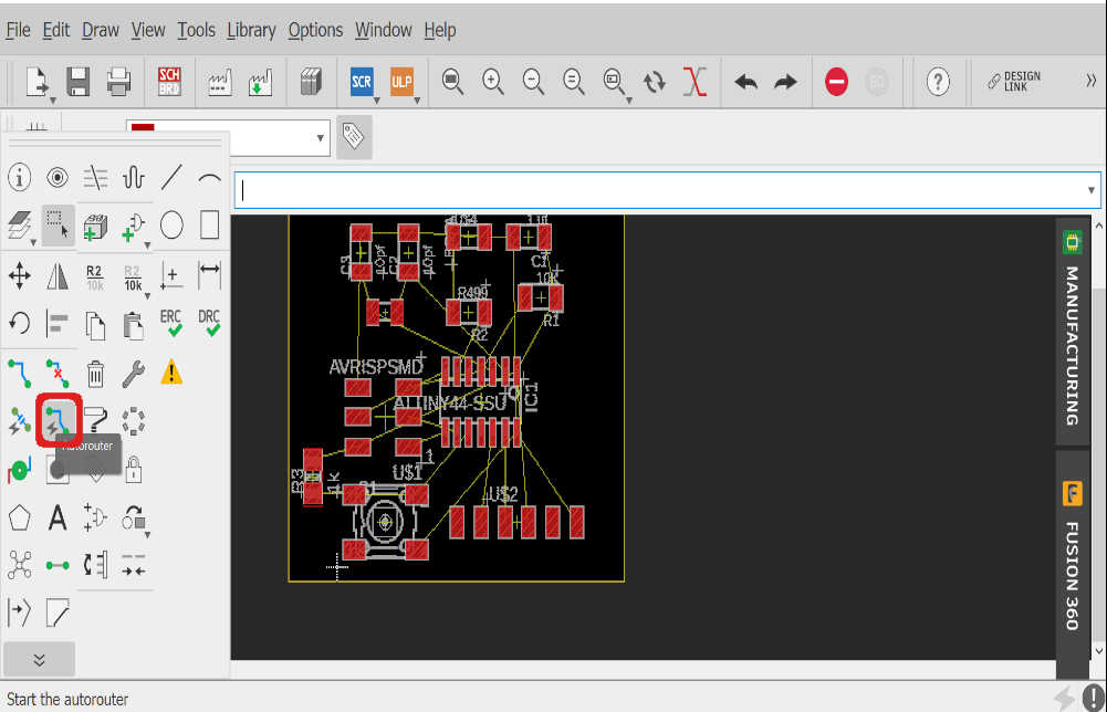
Then click on Start job.
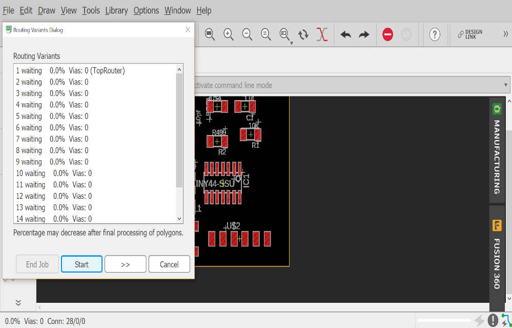
The rule of thumb of routing is that it should be 100%. but incase of less than that some adjustment and manual routing helps.
Some valuable instructions taken from instructors-
Now go to Files-->Export as Image
Use monochrome and export as it is..
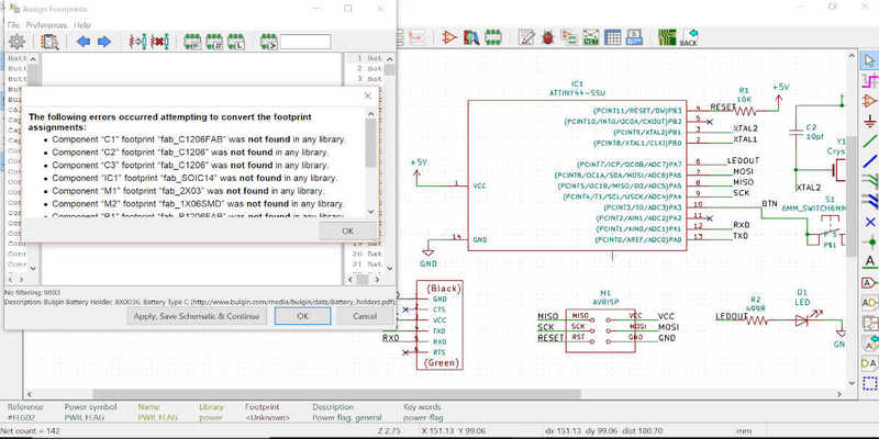
Error Error !!
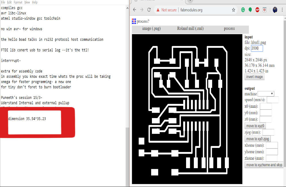
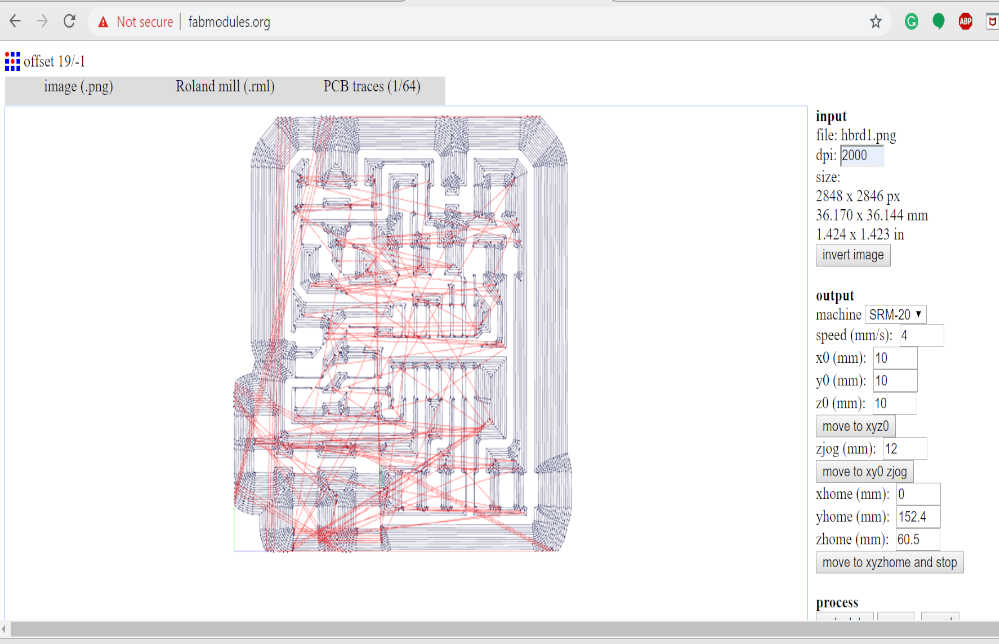
While going throuh my instructors Documentation He instructed to keep resolution high upto 1000 dpi but It was to be fone in FamModules.
But I exported increasing it resolution therby ignoring that it inscreased my size of PCB and blindly generated the .rml files in Fabmods.
If you want to know how to gnereate .rml go to my Electronics Production week from this
link.
The error in dimension led to this..
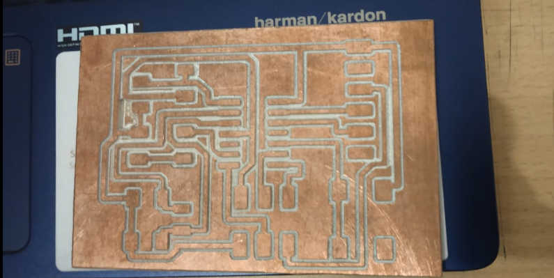
Doing everything again!
So again I exported the file from Eagle this time taking all the dimension in Consideration..
The files for above circuit can be downloaded from here
hello-echo.sch
hello-echo.brd
All files
 we tested out the crystal on an Arduino UNO, we connected the probes to the crystal of Ardunio Uno which showed a frequency of 16 MHz.
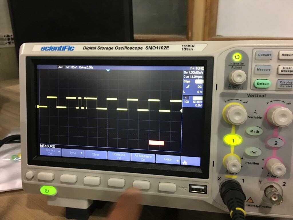 We then uploaded Blink code on the UNO board and we observed the pulse signal.
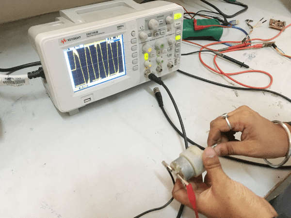 For measuring the analog signals, We connected both the terminals for the motors with the probes of the DSO and then we rotated the motor shaft manually.