Week 9: Embedded Programming
Group assignment:compare the performance and development workflows for other architectures
Individual assignment: Read a microcontroller datasheet program your board to do something, with as many different programming languages and programming environments as possible
In this week I have to learn about microcontroller, read a data sheet and program microcontroller using different programming languages. I have designed a microcontroller PCB during my electronic design week.PCB connected with a LED, Switch and ATtiny44 Microcontroller. First, I have to go through the Datasheet of ATtiny44
The Datasheet has a lot of information about the chip like the pinout configuration, the different registers and timers that are available in the chip. From the first page of Data sheet we get some basic features about the microcontroller such operating voltage, number of timers, registers etc.going inside we get a deep idea about how it works.
I need to share some basic informations that i got while reading the Attiny data sheet.
Before going to that I need to share what is a microcontroller and why we use it.
Microcontroller is a single chip, in which it embbed with some peripherals like the fixed amount of ram, room and memory. The microcontroller is designed to perform some specific functions in which input and output defined, depends on input from some process to need to done and output delivered. Which means microcontroller used for applications which are specific which means uses the small amount of memory, ram and room.
Details About Attiny44
Attiny44 is high performance Low power AVR 8 bit RISC microcontroller.RISC means Microcontrollers that follow Harvard architecture, In Harvard architecture data bus and address bus, are separate so greater flow of data through CPU which gives greater speed. Older microcontrollers are with von numbers architecture. 8-bit microcontroller means CPU can take 8bit of data at a time, means it can take 8bit of data from memory to process.
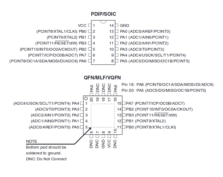
Form the pin diagram we see that Attiny44 have two ports named port A and Port B.PortA (PA0-PA7)is 8bit I/O(input/output ) port with internal pull up resistors.PortB(PB0-PB3) is 4 bit I/O(input/output ) port with internal pull up resistors .
Details are taken from this source
Attin44 have following features of 4k byte In-system programable flash In-System Program-mable Flash,256 bytes EEPROM, 256 bytes SRAM, 12 general purpose I/O lines, 32 general purpose working registers, an 8-bit Timer/Counter with two PWM channels, a 16-bit timer/counter with two PWM channels, Internal and External Interrupts, a 8-channel 10-bit ADC, programmable gain stage (1x, 20x) for 12 differential ADC channel pairs, a programmable Watchdog Timer with internal oscillator, internal calibrated oscillator.
PORTS

I am used this pdf as the refrence document for learning more about ATtiny44
Start with Programming
I had designed a board based on Neil's Echo Hello board in electronic design week . I had added a switch to PA3 switch which is in active low state and PA2 with a Red LED.first i start program the board using avr-gcc compiler. For program thb ISP which i made during the Electronic Production week
AVR-GCC is a compiler that takes C language high level code and produceses a machine code for AVR microcontroller,Machine code lies in HEX format.The programming software reads the hex file and transmits the contained information (the machine code ) into the memory of the Microcontroller
Programming
First i open gedit and create a file named led.c. and type the code mentioned bellow
    // code is copied from Lancy's Fab archive :
    //http://archive.fabacademy.org/2017/fablabkochi/students/157/week8/week8.html

    #include<avr/io.h>               //Import constants related to AVR chip.
    #define F_CPU 20000000            // External clock frequency .
    #include<util/delay.h>            // delay for execution of loop
    int main(void)
    {
     DDRA=0b00000100;                 // Set PA2 as Output port.
     while(1)
       { PORTA=0b00000100;            // LED high at port PA2.
        _delay_ms(1000);             // Delay of 1000 milli seconds.

        PORTA=0b00000000;             // LED low at port PA2.
        _delay_ms(1000);             // Delay of 1000 milli seconds.
       }
    }
Explanation for the code
#include <.avr/io.h> :- Preposser directives that related to your AVR chip into the program which includes pins and Ports. When you compile the program, you must specify the type of AVR chip that you use.
#include<.util/delay.h> :- This includes the function creates short delays in the program execution inside loop.
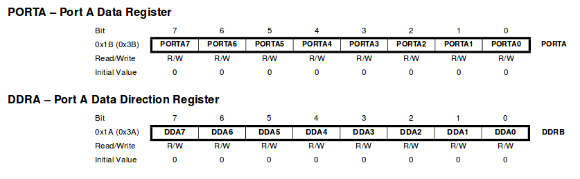
Here i was using Port A its has three registers DDRA,PORTA,PINA.
DDRA means (Data Direction Registor A) here defines the corresponing bit in port A as an input or output respectively. Here in this case 0b represented binary digit representation followed by port specified by one or zero. 1 is defined as output ports and 0 for input. DDRA=0b00000100 means PA2 is output port
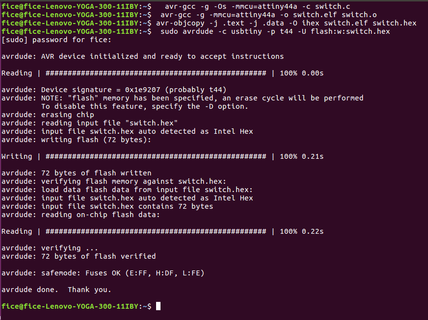
The programming steps using AVR GCC compiler is mentioned below. Open the terminal and enter the following commands.
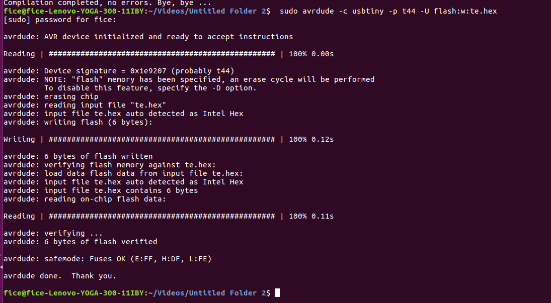
  avr-gcc -g -Os -mmcu=attiny44a -c ledblink.c
  avr-gcc -g -mmcu=attiny44a -o ledblink.elf ledblink.o
  avr-objcopy -j .text -j .data -O ihex ledblink.elf ledblink.hex
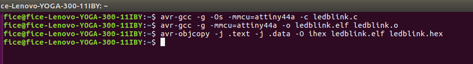
Above three commands generate the hex file, next we need to upload the hex file to microcontroller.
sudo avrdude -c usbtiny -p t44 -U flash:w:ledblink.hex
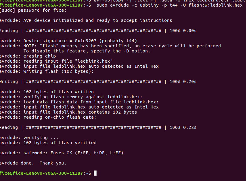
After upload the code LED goes with blinking
Next I write a code to test the switch.My task is to press the switch led goes on and when i release that it turn off.
// Created: March 17 2018
//   Author: Amith G Nair
#include<avr/io.h>
#include<util/delay.h>
int main(void)
{
    DDRA=_BV(PA2); // set PA2 as output
    while(1)
    {
      if((PINA & _BV(PA3)))  // button pressed
      { PORTA=_BV(PA2); //led goes on
      }
      else
      {  PORTA=0;
      }
    }
}
For alternate method we can use arduino Ide for programming. In oder to program ide we need to make some settings change
First we need to add prefernces
go to file--->preferences and add the below link
https://raw.githubusercontent.com/damellis/attiny/ide-1.6.x-boards-manager/package_damellis_attiny_index.json
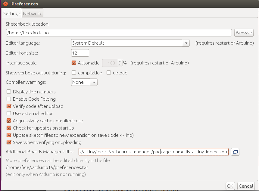
after click ok
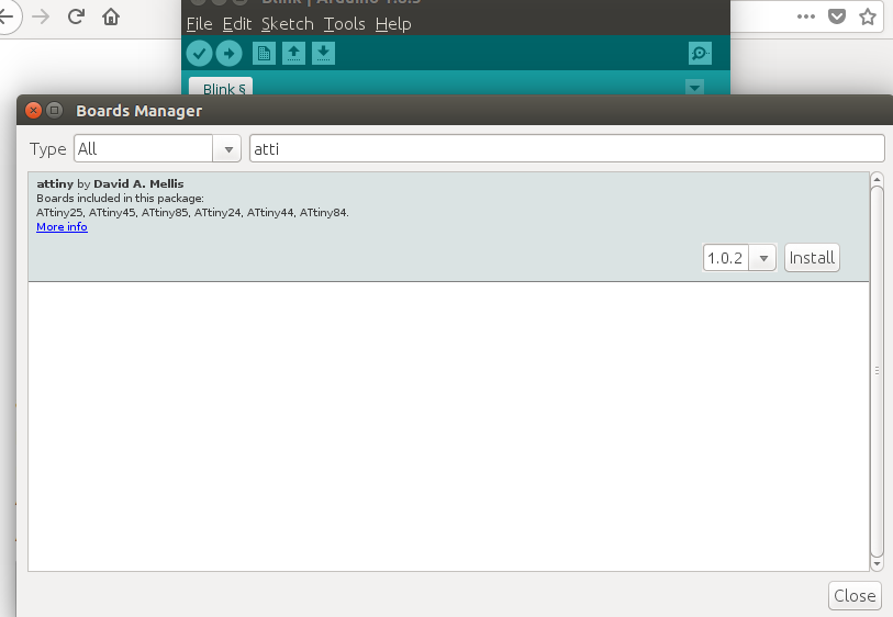
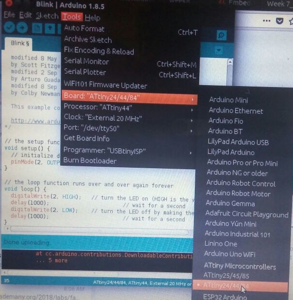
Next go to tools--->Board opens board manager and type attiny and install it.
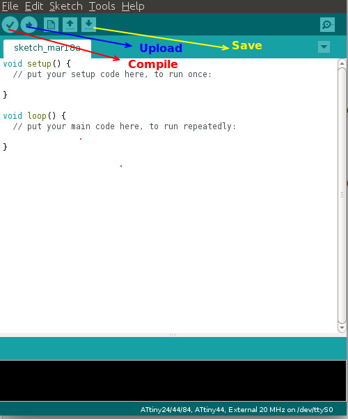
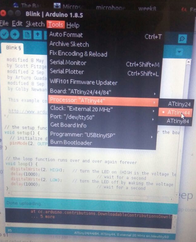
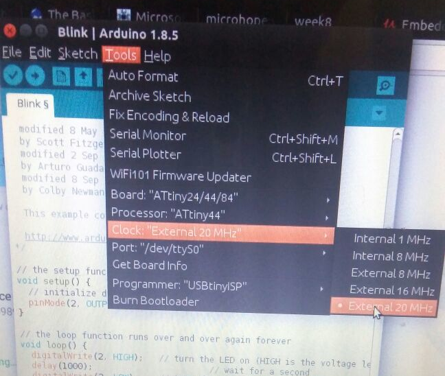
Now our intial step for setting up of arduino ide for Attiny44 over , next we need to upload the the code.Open arduino Ide got tool---> Board as Attiny44.then select processor as Attiny44 ,Clock ---> External 20 MHZ and Select the port
After that we can upload the code,Basic of the arduino coding refer this link click here
 void setup() {
     pinMode(2,OUTPUT); //setup PA2 as outpin pin(LED is connected)
     pinMode(3,INPUT); //setup PA3 as input pin ( switch is connected)
  }
 void loop() {
  int s=digitalRead(3); // Read the status of pin if s=1 when switch is pressed and s=0 when switch is not pressed
  if(s==HIGH)           // Cehck the status of Swith whether its pressed or Not
     { digitalWrite(2,HIGH);   turn on led
      }
  else
      { digitalWrite(2,LOW);   // turn off led
      }
  }
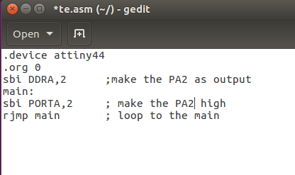
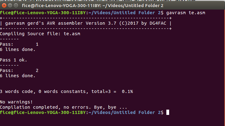
Next I go with assembly line programming in my attiny board
First i need to install gavrsm to compile the assembly code, first download it form this link and extract the file and place in in bin folder .Before Assembly programming i used this links to refer how to write code link1 and link2
Open the gedit and type the below code and save it as .asm file
Mode details reagrding working with ATtiny44 go to refer input week
Microcontroller
Microcontrollers are often described as single-chip computers. They contain a microprocessor core, some memory and various devices such as parallel i/o ports, serial i/o ports, timers, analogue to digital converters (ADC's) etc.
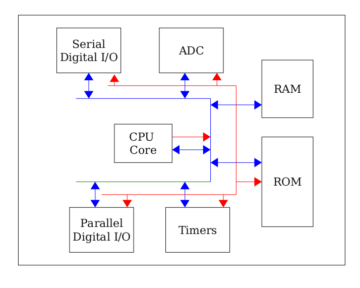
CPU
The central processor unit is responsible for executing stored program (in ROM) and managing the peripherals. It fetches numeric instructions from memory (opcodes) one by one, interprets them and carries out some operation as a result. CPU mainly consist of some components like Registers, ALU and Instruction Decoder .Details are taken from this source
Registers are a little like internal memory storage areas. These are useful for interim calculation results.The arithmetic logic unit is responsible for carrying out calculations.In some CPU's this can be quite simple; perhaps only supporting add, subtract and basic logical operations.instruction decoder's job is to translate numeric opcodes into sequences of actions.
Data bus is a collection of wires that are used to transport numbers into and out of the CPU. A logic '1' on each line of the bus is represented by a particular voltage commonly 5V or 3.3V. Logic '0' is commonly represented by a 0V signal.
Address bus is another collection of wires used to select which of the memory locations is allowed to use the data bus.
RAM & ROM
RAM -random access memory is used for storing values that are liable to change during the course of the execution of a program.RAM contents are usually lost each time systems are turned off/on.
ROM -read onlymemory does not lose its contents when power is removed. Thus it is generally used for storing programs .
Serial I/O
Serial communications requires the sender to send data 1 bit at a time a rate agreed with the intended receiver. Each bit is given a time slot, the sets the transmit wire to the correct logic level for each bit's time slot. The receiver measures the voltage arriving from the sender at the middle of each bit's time slot. It can thus decide whether a '1' or '0' has been sent for a particular bit.
Parallel Digital I/O
microcontrollers send and receive information to the outside world using ports. There are many different types of port however the simplest is the parallel I/O port. These ports can be thought of as memory cells or registers that are connected to the CPU core using the data bus and also tothe outside world via pins on the side of the microcontroller.
Timers
Timers are typically constructed using a clock source and a counter.Counters count clock periods that are input to them.
ADC's and DAC's
Frequently microprocessors are required to process non-digital .analogue (or continuous) signals. In order for them to do this, a special device called an Analogue to Digital Converter is required.This device accepts an analogue input and translates this to a digital number.
Interrupts.
Very simple microprocessor systems are often built which execute only one task.
PIC Microcontroller
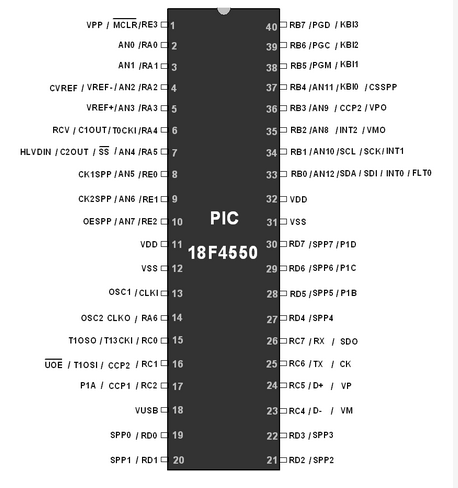
PIC is a family of microcontrollers made by Microchip Technology.PIC micro chips are designed with a Harvard architecture, and are offered in various device families. The baseline and mid-range families use 8-bit wide data memory, and the high-end families use 16-bit data memory. The latest series, PIC32MZ is a 32-bit MIPS-based microcontroller. The PIC architecture was among the first scalar CPU designs and is still among the simplest and cheapest.
PIC18F4550 device in PIC18 family. PIC18F4550 is an 8-bit RISC architecture microcontroller. Its specifications are
Details are taken from this source
- Timer: One 8-bit and three 16-bit Timers i.e. Timer0-Timer3.
- USART: 1 In-built Enhanced USART.
- ADC: 10-bit 13 channel ADC.
- Capture, Compare and PWM module (CCP) and Enhanced CCP module.
- USB: USB V2.0 support transfer speed 1.5Mb/s to 12Mb/s.
- Master Synchronous Serial Port (MSSP) having I2C and SPI protocol.
- 256 Bytes of EEPROM, 32Kbytes of Flash memory and 2KB internal SRAM.
- PORTS: A, B, C, D and E.
- Streaming Parallel Port for USB streaming transfers.
- Three External Interrupt.
- Oscillator:
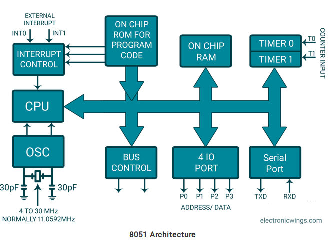
8051 Microcontroller
The 8051 is the first microcontroller of the MCS-51 family developed by Intel Corporation in 1980. It was developed using N-type Metal-Oxide-Semiconductor (NMOS) technology, and later it came to be identified by a letter C in their names, e.g. 80C51 which was developed with Complementary Metal-Oxide-Semiconductor (CMOS) technology which consumes less power than NMOS and made it better compatible for battery-powered applications.
Details are taken from this source
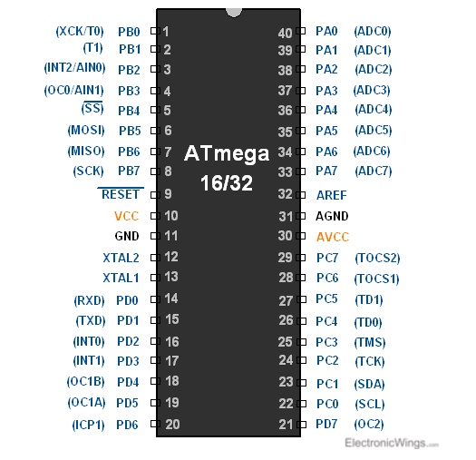
AVR Atmega 16
ATmega16 is an 8-bit high performance microcontroller from the Atmel’s Mega AVR family. Atmega16 is a 40 pin microcontroller based on enhanced RISC (Reduced Instruction Set Computing) architecture with 131 powerful instructions. It has a 16 KB programmable flash memory, static RAM of 1 KB and EEPROM of 512 Bytes. The endurance cycle of flash memory and EEPROM is 10,000 and 100,000, respectively AVR ATmega16 has 32 pins constituting four ports.PORT A,PORT B,PORT C,PORT D.Each port has 8 pins.these pins of these four ports can be used as general purpose inputs/outputs.
Details are taken from this source
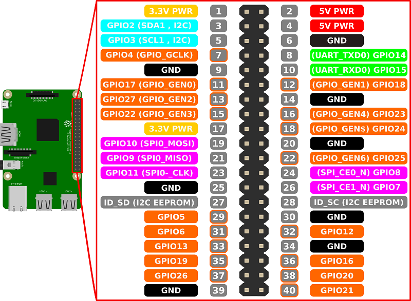
Raspberry PI
Raspberry pi is small single board computer that is designed to teach basic computer skill fo school students in developing countries.Now there are wide varity of Raspberry pi models and they are used in various feild.
Raspberry pi is equiped with processor of BOARDCOM , which is of ARMv6 architecture.ans we can program using Python ,c java etc
Basically i used Raspberry PI 3 board , which is equiped with 1GB RAM, four USB ports, 40 GPIO pins, an Ethernet porta and build in wifi , bluetooth module build in camera connector etc. Arm processor is the brain on the raspberry pi which helps to work it smoothly
Details are taken from this source
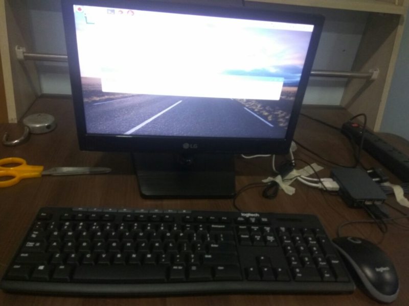
First i do with my office PC made using Raspberry pi and then i share the knowledge with my colleagues in fab academy

In order to control the GPIO pin of the Rpi,we will use the RPi.GPIO python library.This library allow user to easily access the GPIO port without having to know low-level programming.We are instlled Raspbian OS in Raspberry pi so RPi.GPIO library is included in that, and its not loaded by default so we need to import it to program.