Week 5: Electronics Production
Group assignment: characterize the specifications of your PCB production process
Individual assignment: make an in-circuit programmer by milling the PCB
Electronic Production:
Printed Circuit Board is very important for all electronic equipments like cell phone Tv fridge etc . Apart from electrically connecting, it also gives mechanical support to the electrical components.Informations are collected from this source
What is PCB?
PCB is just a non conductive board on which copper trackes are carved instead of wires.These tracks are joined at various nodes.
PCB Production :
I have little bit knowledge in PCB designing and making. I Mainly used proteus for designing PCB and Making PCB Using old etching method with help of ferric chloride solution.
Steps I used for PCB Making duing college time
- Draw the design using Proteus file and export the PDF file
- Print Out the Design I from laser printer into the Shiny Side of the Photo sheet Paper
- Sand the copper clad using sandpaper so There Is a Rough Surface for the Design to Stick When Transferred. Clean the Copper Clad sheet I mainly used Epoxy type it's quite good. We can use any washing powder to clean the surface and Let It Dry using clean cotton.
- Place the design face down to copper, Run the Hot Iron box over the Plate With the Design Face Down. Do until lite black colour appears on the visible side of design paper.
- After Running the Plate Through an Iron Place the Cooper clad Into a Cold Bath and Agitate Until the Paper Floats Off.
- Place the PCB Into the Etching Solution ( Ferric Chloride ) and Agitate for 25-30 Minutes
- Once All the Copper Is Gone Rinse It in the Water Bath, Let It Dry and Use Rubbing using nail polish to Whip Off the Ink Transferred Onto the PCB after that use a pcb driller to drill the holes.
I was doing too much time for PCB making and also the chemical waste after etching also harmful to the environment. But one important thing I understand that we can't use the FR4 copper clad sheet in Modella Mdx, because here processes of making PCB are craved the unwanted paths, so if we use FR4 type copper clad it creates tiny fibre particle it causes respiratory problems.
About Modella MDX 20
Roland Modella MDX-20 is a desktop CNC machine used for making PCBs, carving moulds with soft materials like wax. It is compatible with most of the 2D and 3D CAD software. It has a small bed which moves in the Y-axis, a Tool head which moves in the X-axis and the end effector which moves in the Z-axis. It supports many milling bits and is versatile. Informations are collected from this source
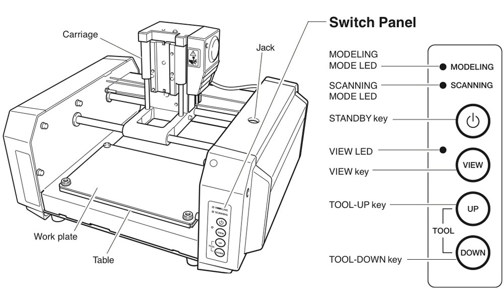
Above image is copied from Media Lab Helsinki
Toolup key and Tool down key is used to control the z-axis movement of the tool head. Jack holder, there is a sensor that detects if the machine cover closed or not, the machine does not operate if we don't close the lid.
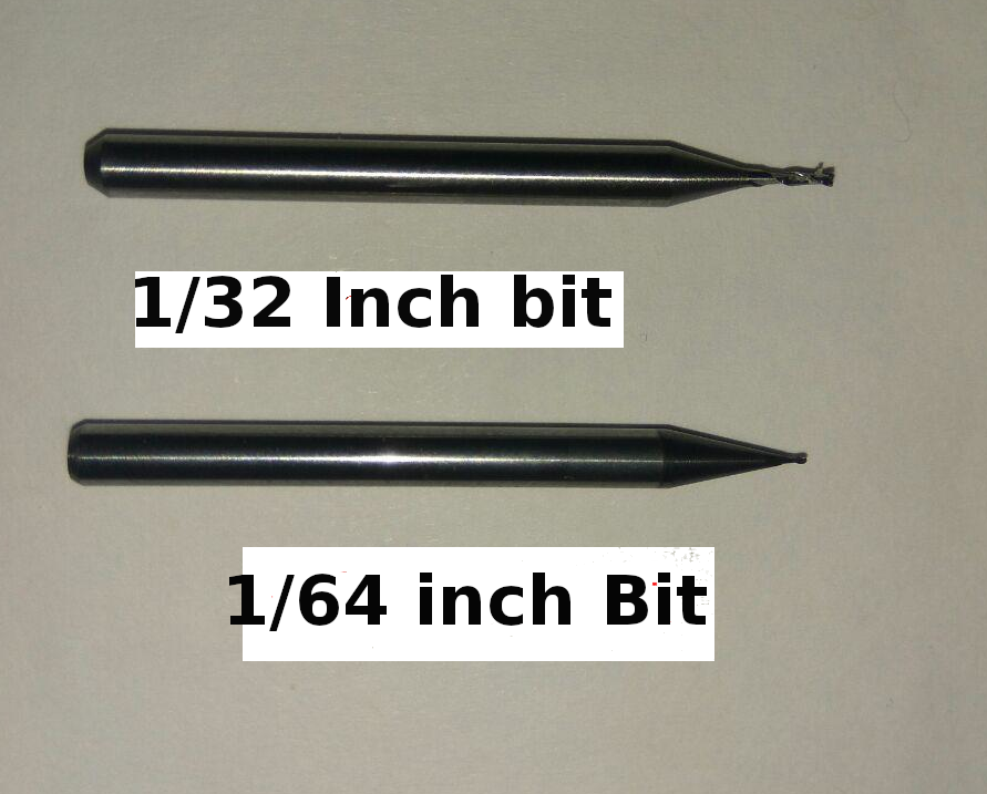
For PCB milling operations machine mainly uses two types of bits 1/64inch and 1/32 inch. 1/64 inch I used for milling the traces. And 1/32 is used for cutting and drilling purpose. The bit is fitted in the head and tighten using Allen key. Kept the bit in sound tight, small vibration or loose may tend to broke the bit also damage the pcb, so mounted the bit with sufficient length.
The machine has a bed, and in that, we placed the sacrificial layer, Before start operation on the machine check the alignment of bed, is it adequately placed or not, any small alignment problem also led to broken the bit. We put the copper cad on the sacrificial layer using double sided tape and set it clearly and avoid air bubbles inside that.
Before starting the milling work we need to fix a sacrificial layer on top of the bed,every one ask why we fix this layer , our instructrs said that if the bit goes down below the depth of PCB if there is no sacrificial layer bit will contact with steel bed and it tend to damage.
Group Assignment
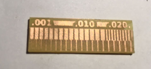
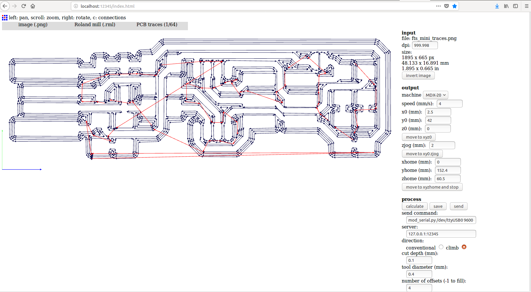
In this Assignment we need to characterise the process of making pcb using our machine, So that can find how much thickness our machine can Mill, Here we are using 1/64 inch bit for Milling purpose. First, we download the image from academy page and use the offline fab module to mill the pcb.
Milling operations are carried out by3mm/s speed , offset of 4 and offset overlap at 50%. We observed that thickness less than 0.1mm the traces are imperfect.for this we understand that we can only make traces above 0.1mm using 1/64 bit and the clearance between the traces, the machine did not mill out the portions where the width was less than 0.4mm.
From this we concluded that traces must have a size greater than 0.1mm and the clearance between the traces has to be kept at least 0.4mm.
Individual Assignment
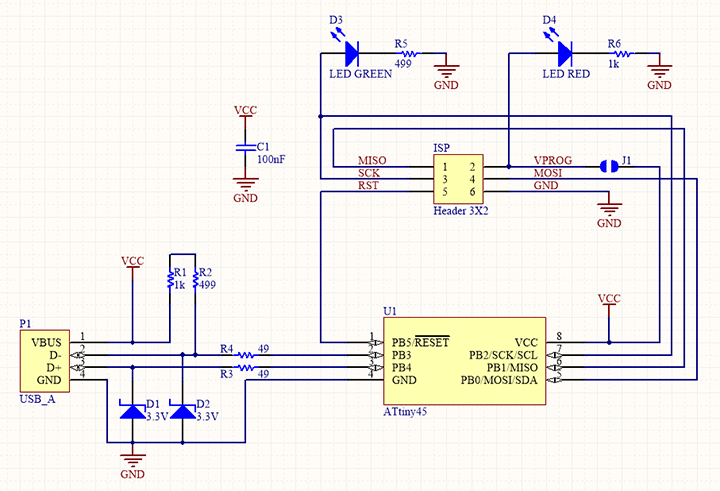
We need to make a ISP ,I chose to make the Brians, FabISP because I felt the documentation along with it was very well written, and easy to understand.
ISP
In Application development for embedded systems is usually done by computer using assembly languages or high level languages like c ,c++ etc.After creating the executable binary code, we need to upload that to target development board. In earlier days chip had been removed from the target board and placed in a programming device, but nowadays chips can be reprogrammed without being removed from the circuit.
Here we are making AVR In system programming device ,FabTinyISP design is quite simple and it looks like usb ,on the PC side it connects to the USB port. We are using Attiny 45 chip for ISP programmer.
Making ISP
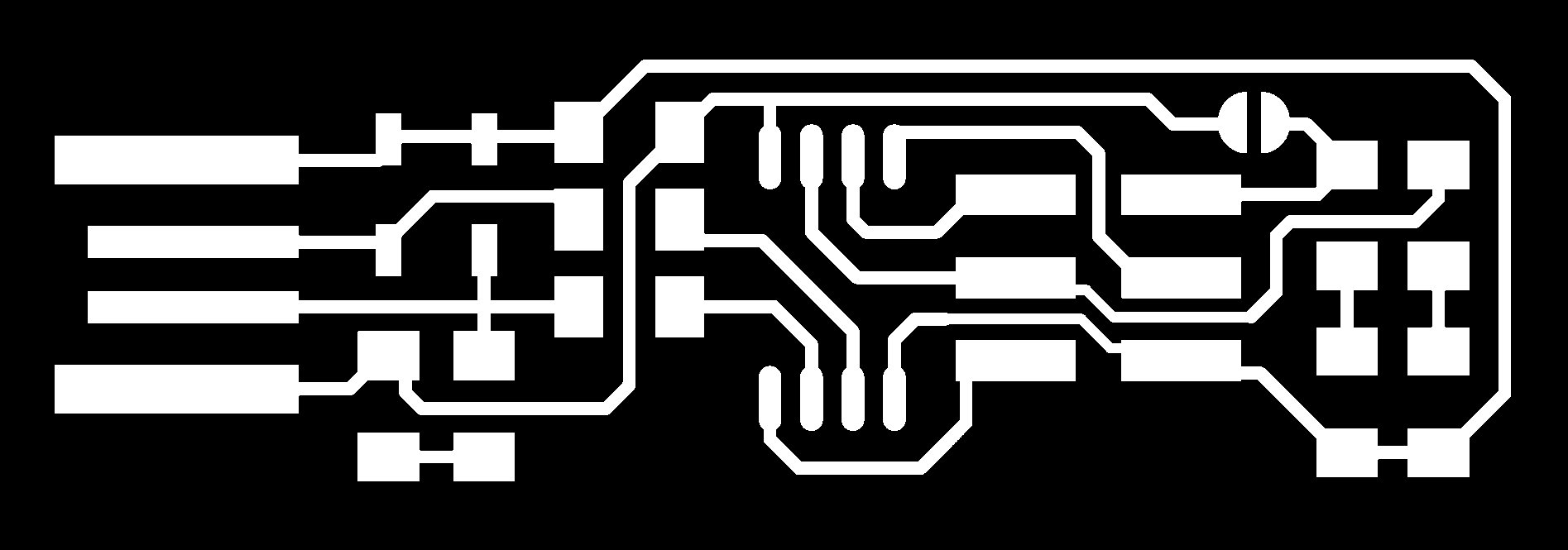
First i download the milling image and cutting image from brians website. We are using Modella MDX 20 for milling purpose , her work is done using two stages
PCB Fabrication
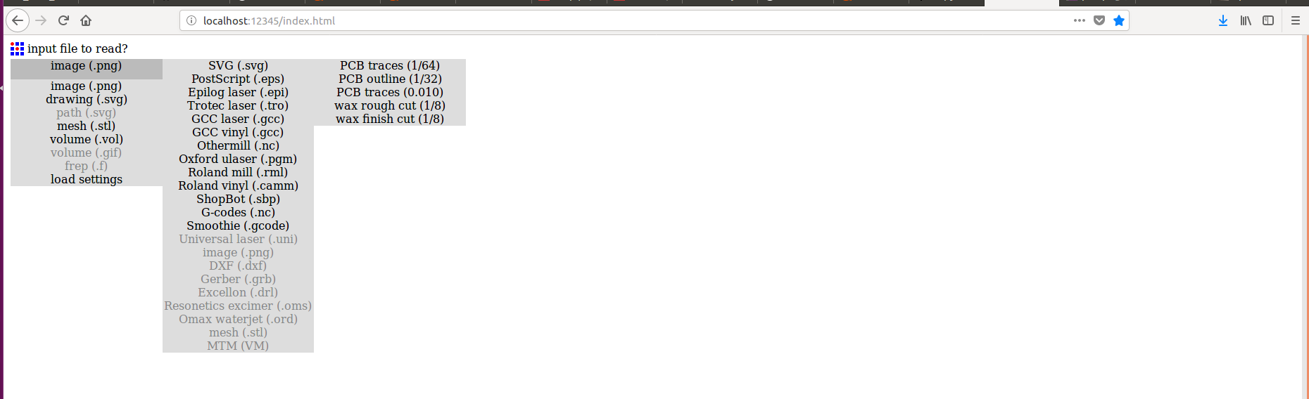
Here we are starting with offline version of fabweb module for pcb milling using Modella MDX 20, we are running mods locally in our fab computer so in order to start we type fabweb in terminal windows
Then go to firefox and type localhost:1234/index.html then mods window will open on the firefox.
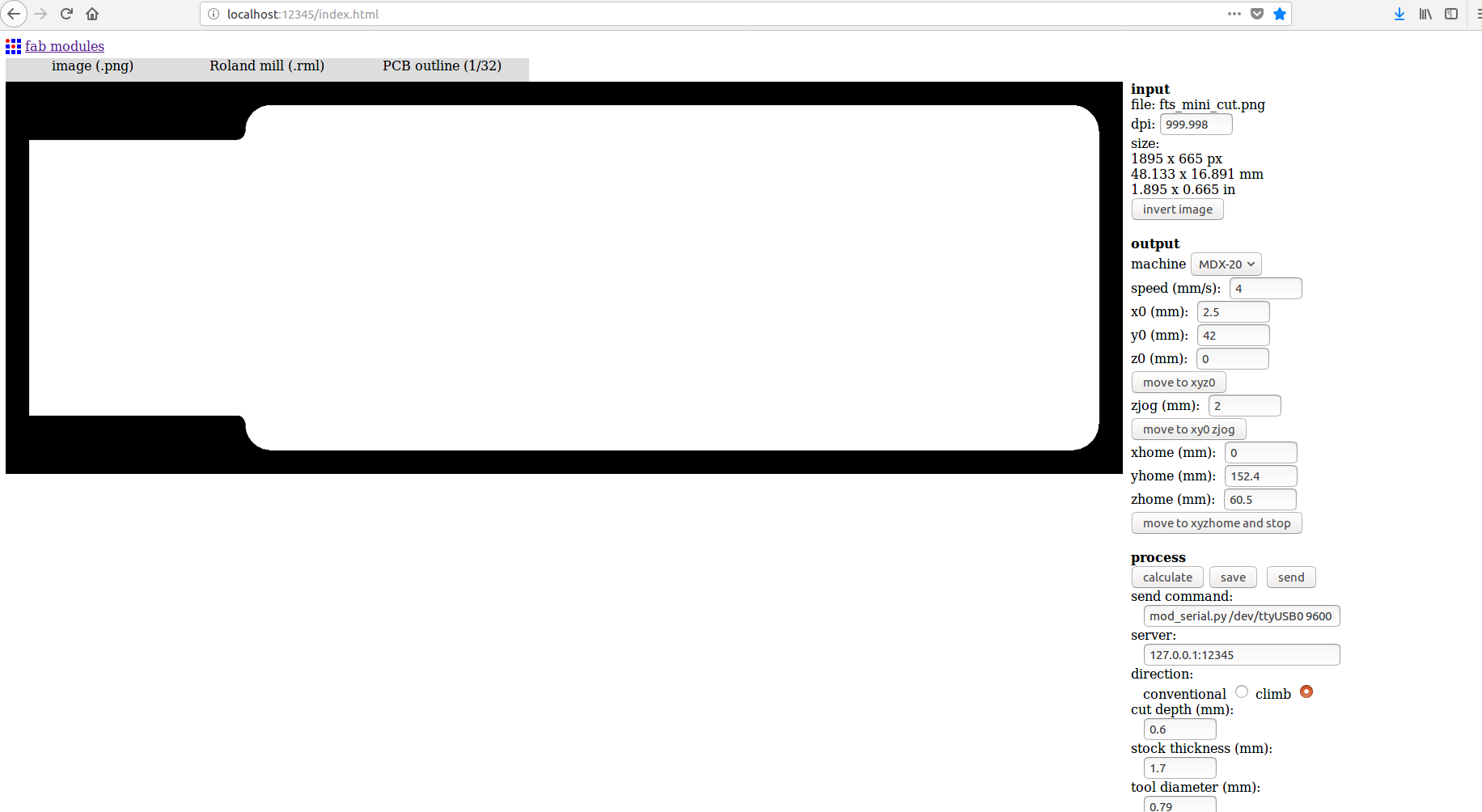
Then we load input format with png file we need to trace,outpurt format as Rolland Mill.rml and process as pcb traces 1/64.
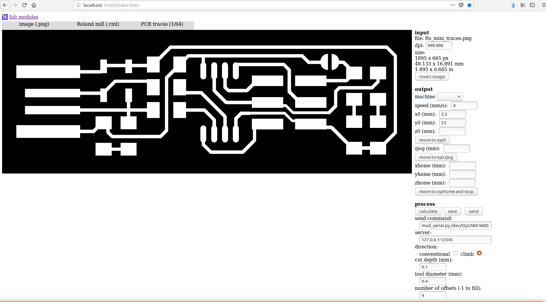
After that we ofset the tool origin by changing the values of x0 as 2.5,y0 as 42 and z0 as 0 ,in order to machine the available space.Then click move to xyzo button , then machine go to corresponding location then i fitted machine with drill bit and adjust for my needs .
After that i press calculate button to claculate paths which bit will move and then click on send button to send the machining instruction to modella for performing milling.
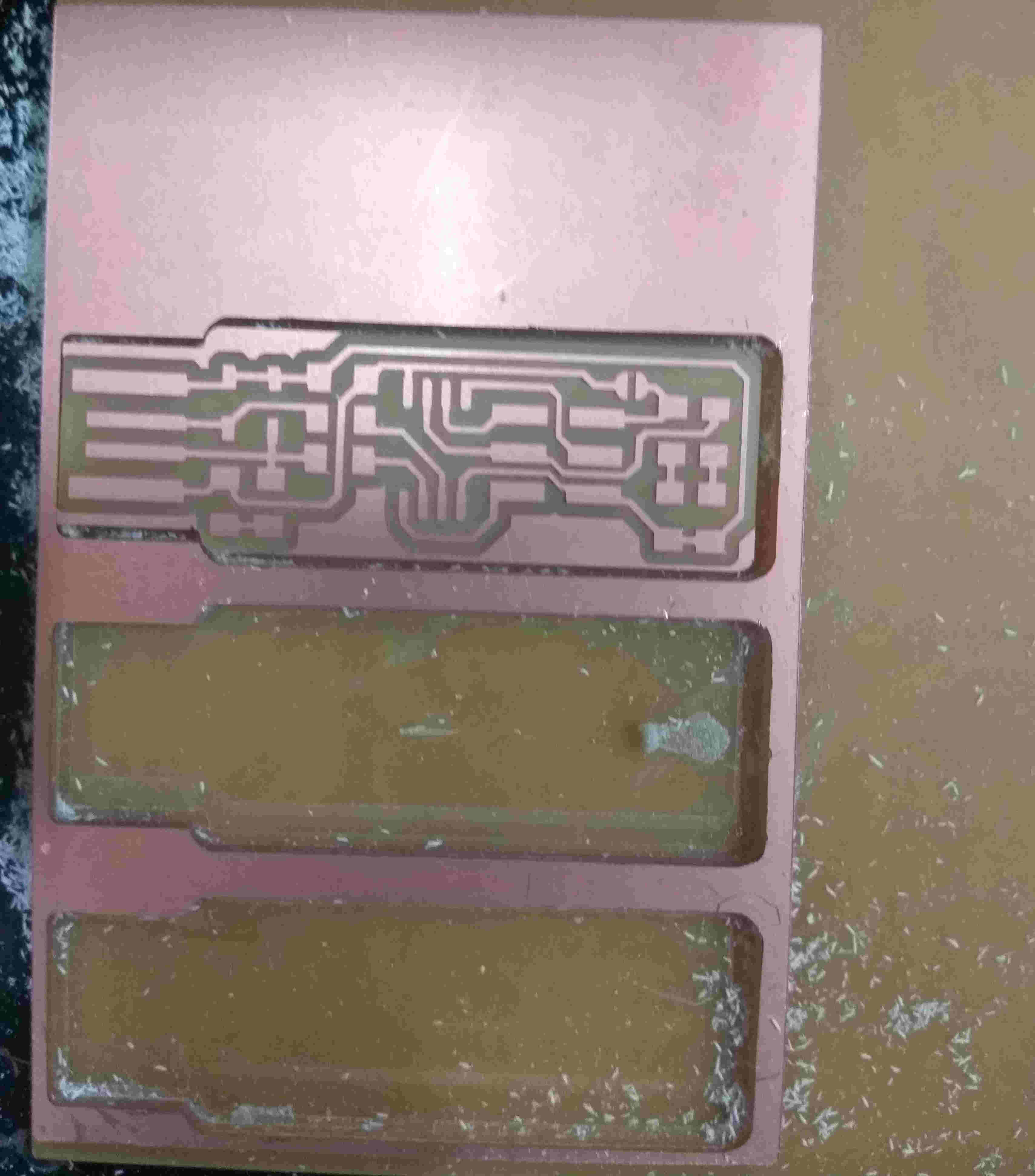
After perform the milling the same process is repeated for cutting on thing is intially we need to change process as pcb outline (1/32) .

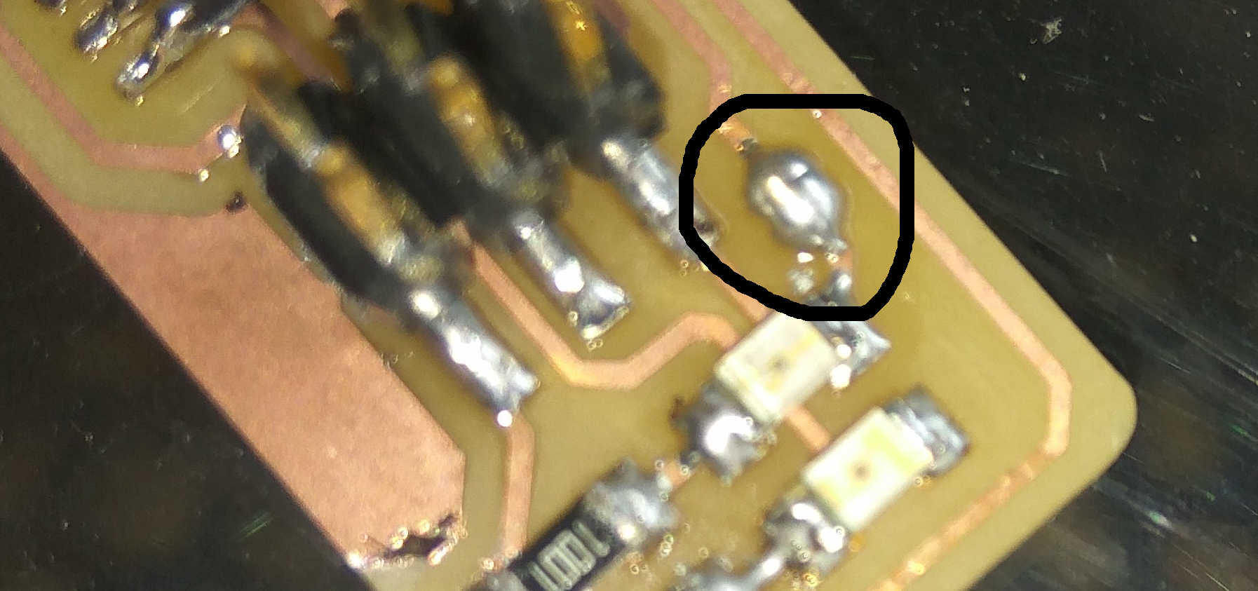
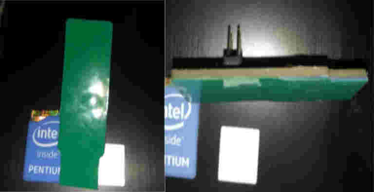
After perform the milling and cutting we need to solder the pcb with componets, before that we need to remove some copper from the usb tip. otherwise when we connect it to usb it makes usb short and it get restart
PCB Soldering
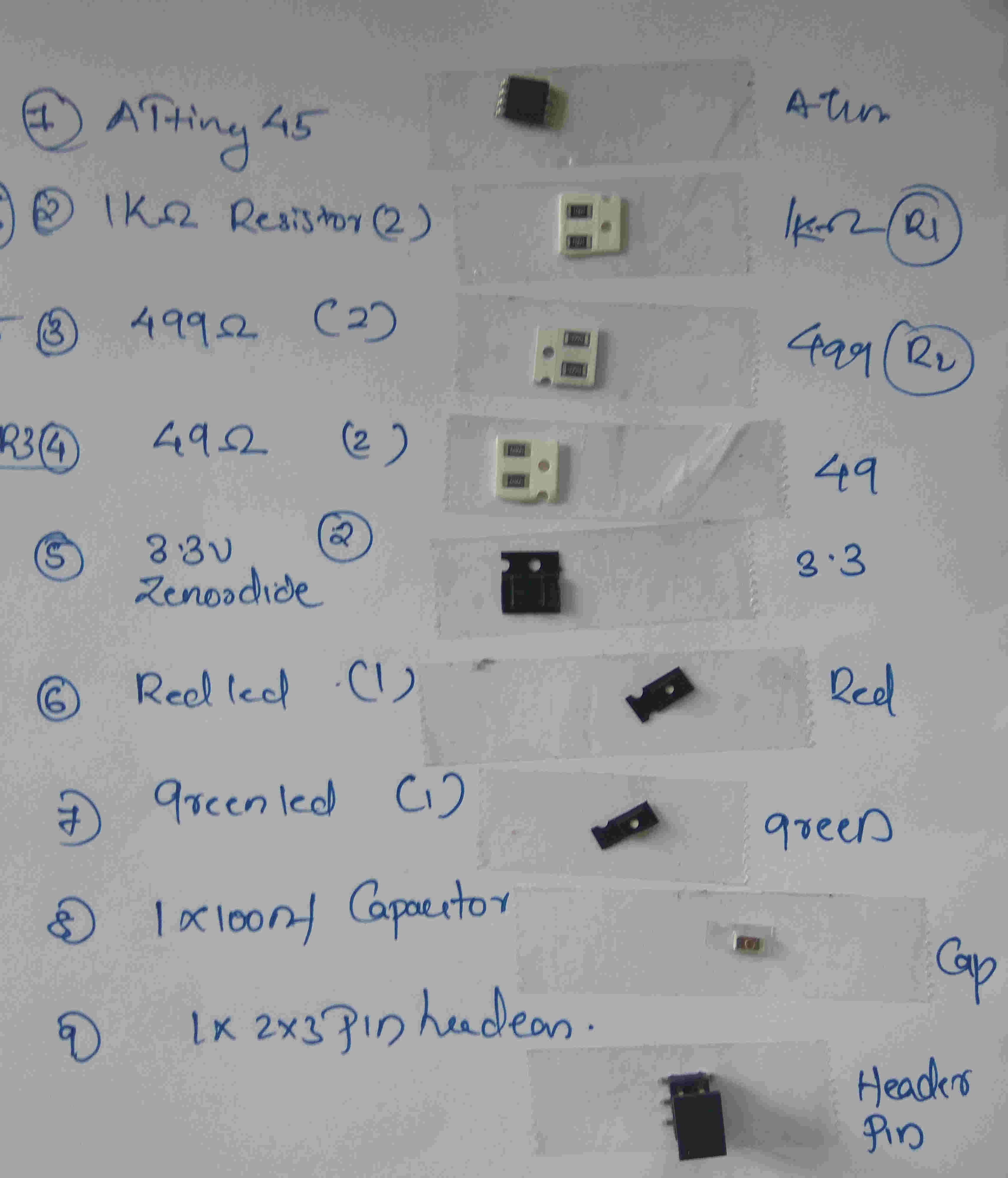
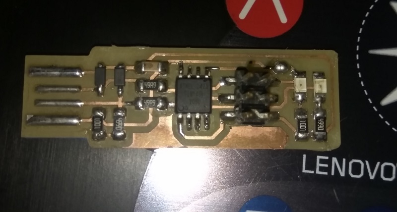
After perform the milling and cutting we need to solder the pcb with componets. First i take a paper and name the compont list and collect that from shelf.
list of components
- Attiny 45
- 2x3 pin header
- Resistors of 1k ,499 ohm,49 ohm
- 3.3v zenor diode
- 100nf capacitor
Ensure that pcb is clean from dirt otherwise solders will not stick appropriately with the traces. Put little bit solder on the traces and then place the component on that and then touch each point with solder iron it will stick on that, and after that, we can add little bit solder to the ends.
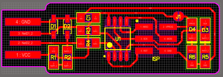
During soldering we need to create a bridge between J1 This temporarily connects VCC to the Vprog pin on the ISP header so that the header can be used to program the tiny45.
After completingthe soldering,I used Multimeter to check the connection , any shorts occuring between vcc and gnd etc.
Before going to the program I need to do some physical changes to my ISP to make a suitable USB connection we need to do some changes. First, I flow some solder over the USB contacts on the board to build them up a little bit. and then place a thin layer of vinyl over back side of pcb to make it ticker otherwise it doesn't fit properlly
Programming the fabisp
Steps for programming is explained in this link . First we need to setup enviroment for upload and building firmware , we need avr-gcc installed in Ubuntu.I execute below command in terminal to execute the avr-gcc installation in my computer
sudo apt install avrdude gcc-avr avr-libc make
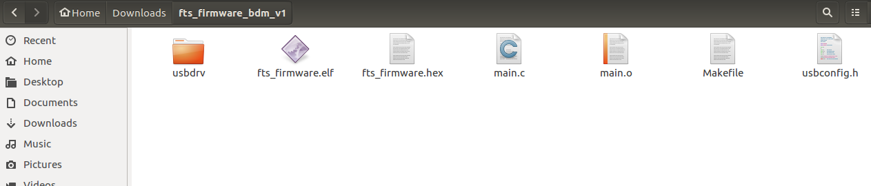
Next we need to downlaod the firmware from the link provide in Brian tutorial and then extract the link and open the folder in terminal and run make command
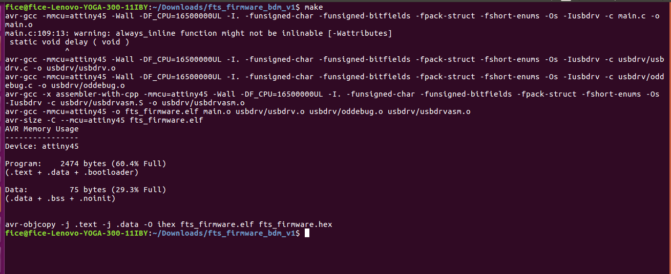
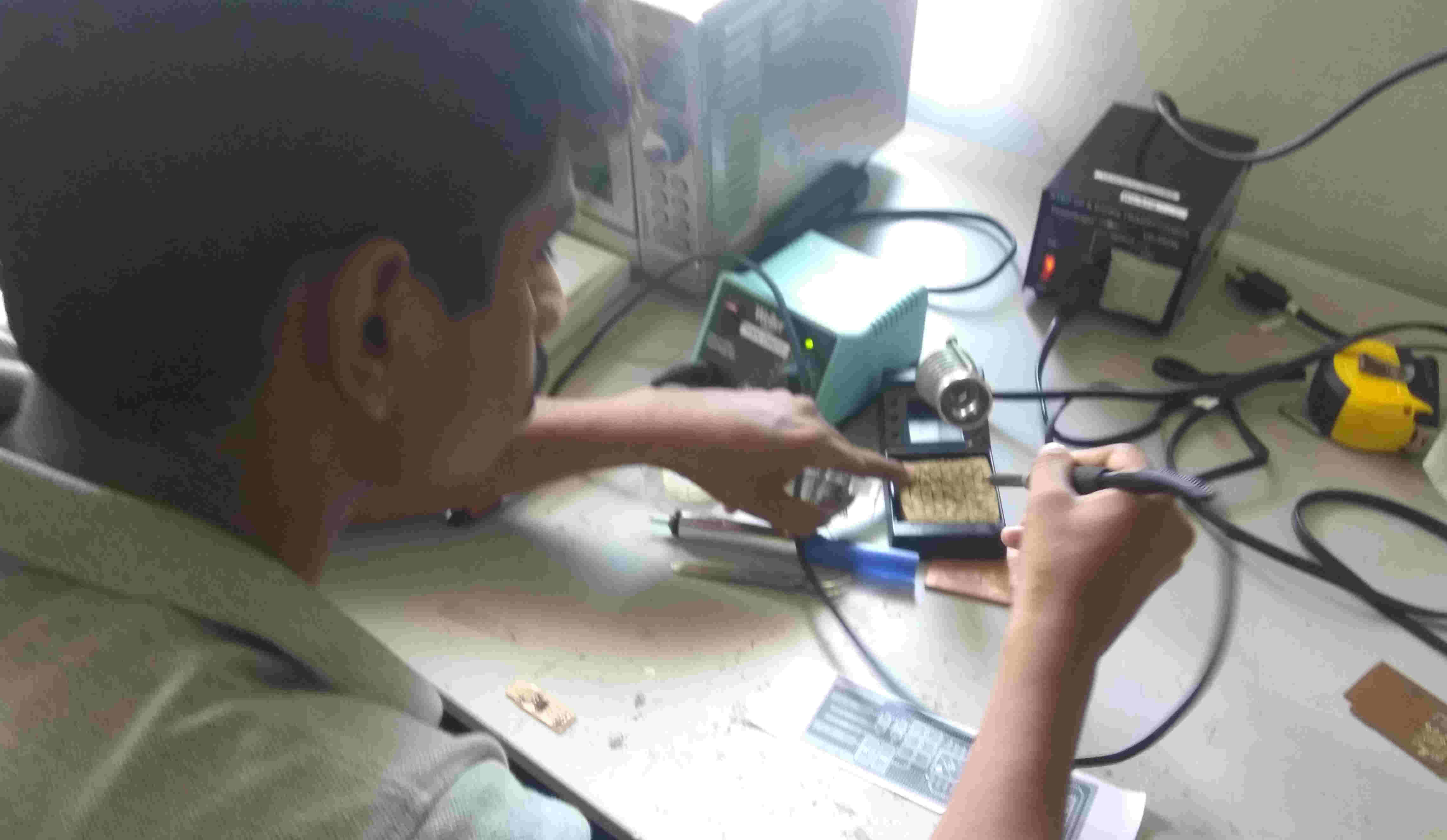
run make command ,this will make hex file to program the fabisp .Now we should have a file named d fts_firmware.hex. Then i connect the ISP from Akil hari in usb port 2 and connect to my pcb with ribbion wire.
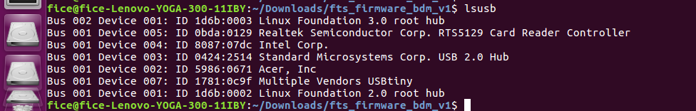
Then open the terminal and type lsusb which list the connected usb , Akil hari is detected as multiple vendors Usbtiny. Then type make flash This will erase the new chip, and program its flash memory with the hex file we created .
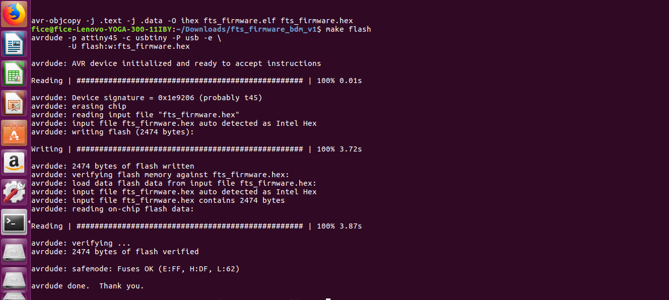
After that we type make fuse command ,it will set up all of the fuses except the one that disables the reset pin.
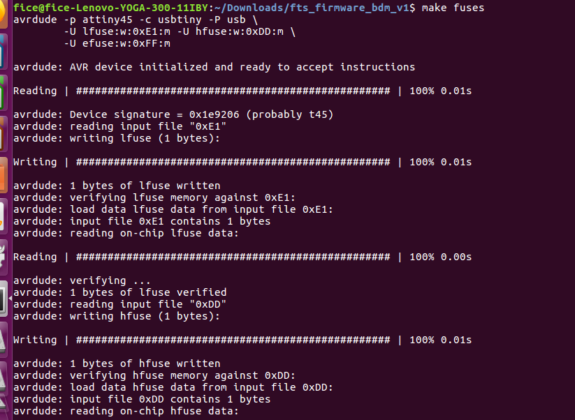
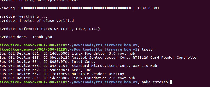
Then i remove the akils isp and also remove the ribbon connection, then connect my ISP to laptop and check by typing lsusb it also show the same result ISP is detected as Multiple vendors Usbtiny . Then i confirm thet its working .
Now, we need to blow the reset fuse, so that ISP cant be programmed again and also to convert the reset port to a digital I/O port- in order to do this type rstdisbl command in terminal and hit enter.
Fab ISP made in this week is used for used for programing the MCU boards developed in Embedded Programming, Input week, Output week, Interface and application programming, Networking and Communications and Final Project