Week 6
Electronics Design

assignment
Group Assignment
- use the test equipment in your lab to observe the operation of a microcontroller circuit board
Individual Assignment
- redraw the echo hello-world board
- add (at least) a button and LED (with current-limiting resistor)
- check the design rules, make it and test it
- extra credit: simulate its operation
- extra credit: render it


Hello world eagle file .SCH Download
Hello world image file .BRD Download
Hello world gcode .NC Download
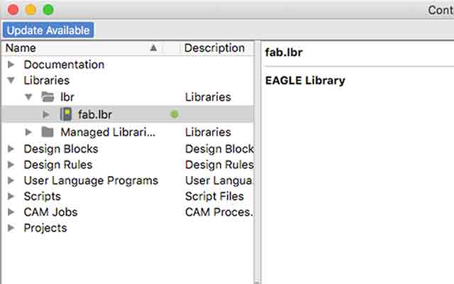
The first thing I had to do was create a board file using Eagle. I began by downloading and installing a library that includes the components I would be STUFFING the board with.
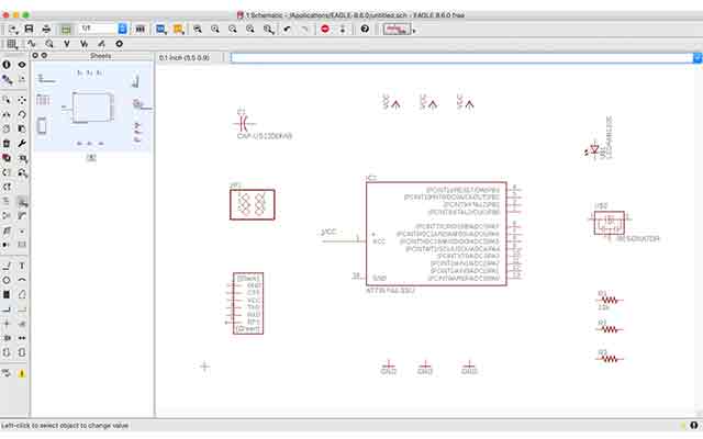
This is a great piece of software that allows you to create pcb layouts and connect them and test whether the circuits will work. You can do commands like:
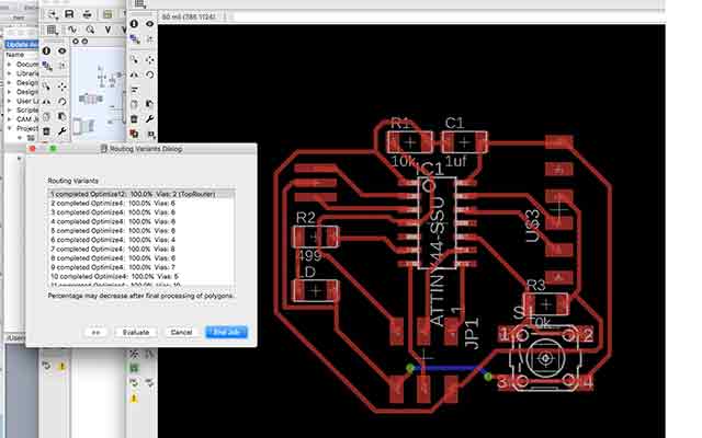
With a bit of patience I was able to recreate the board in the tutorial. I used auto-generate but it didn't resolve the paths so I had to manually position many routes.
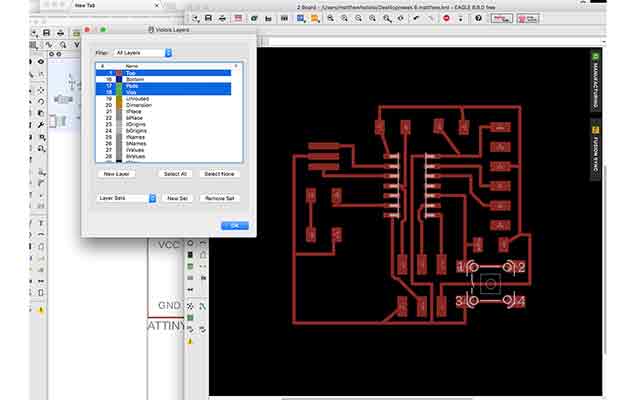
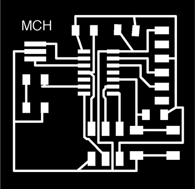
Then I printied a .png (not export) and produced a .png that is to scale
MILL IT
I used our milling machine which doesn't have any sensors to cut out the paths. I made sure the bed was flat without any debris ontop. Next I manually positioned the head just above the copper board, loosened the bit and let it touch the surface of the board. Then I tightened the bit and set all the axis to zero. I clicked start and the mill cut out the paths into the copper board just as designed.
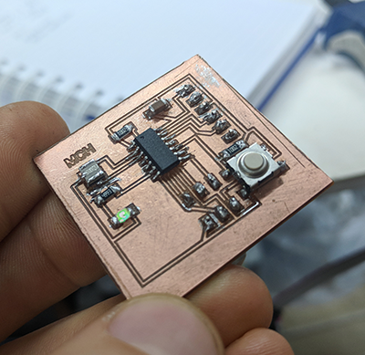
STUFF IT
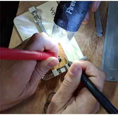
Just like in Eagle, I went through the library of components and this time laid them out physically. It was a lot easier this time as I had done it before in Week 4.
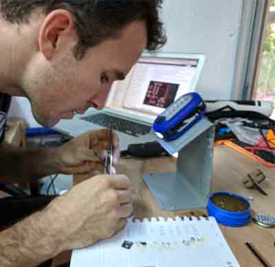
In between components I would use a Voltmeter to test pathways and make sure there were only desired connections making contact.
I decided to put the pins through the board and have the pins on the bottom because it would be easier for them to stay attached to the board.
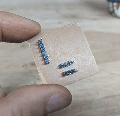
This time took me only a few hours of soldering to make the board.
With my new board I plugged it in to our new AVRISP mkII (this tool is very useful for troubleshooting and identifying bad solders) and the light stayed red. I checked my connections and cleaned up any soldering that looked conspicuous. I tested paths with the voltmeter and after a few minutes of cleaning edges I had the light green.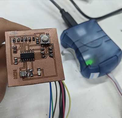
- use the test equipment in your lab to observe the operation of a microcontroller circuit board
Individual Assignment
- redraw the echo hello-world board
- add (at least) a button and LED (with current-limiting resistor)
- check the design rules, make it and test it
- extra credit: simulate its operation
- extra credit: render it
Software Used
Eagle, Art Cam, Grbl Controller, Adobe Illustrator, Google Chrome, Sublime Text, Photoshop, Git, Arduino
Tutorial Used
Fab Academy Week 6 - Electronics DesignFiles used:
Hello world eagle file .BRD DownloadHello world eagle file .SCH Download
Hello world image file .BRD Download
Hello world gcode .NC Download
Walkthrough
DESIGN ITThe first thing I had to do was create a board file using Eagle. I began by downloading and installing a library that includes the components I would be STUFFING the board with.
This is a great piece of software that allows you to create pcb layouts and connect them and test whether the circuits will work. You can do commands like:
 Install a library of components.
 |
 Lay out a visual plan of a PCB.
 |
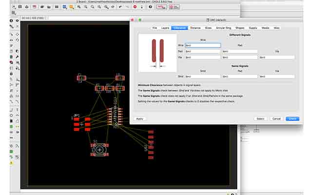 Adjust minimum clearance on paths.
 |
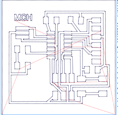
With a bit of patience I was able to recreate the board in the tutorial. I used auto-generate but it didn't resolve the paths so I had to manually position many routes.
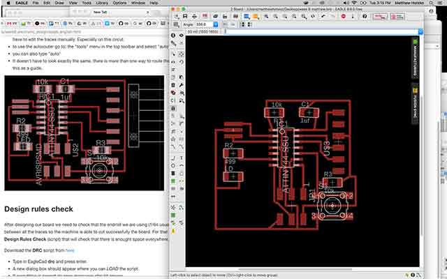 I modified some of the routes slightly. |
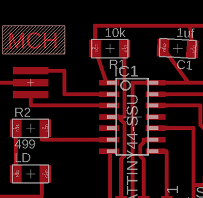 I also added my initials to the board. |
Then I printied a .png (not export) and produced a .png that is to scale
MILL IT
 I visited the fabmodules.org page and uploaded the PNG drawing. |
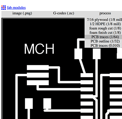 I selected my desired output (GCODE) and specified my cut size (1/64) |
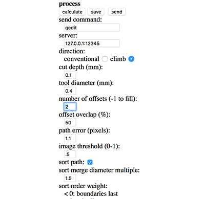 I edited the number of offsets to make sure I had clean paths cut. |
 Then I clicked calculate and the program generates the gcode file. |
I used our milling machine which doesn't have any sensors to cut out the paths. I made sure the bed was flat without any debris ontop. Next I manually positioned the head just above the copper board, loosened the bit and let it touch the surface of the board. Then I tightened the bit and set all the axis to zero. I clicked start and the mill cut out the paths into the copper board just as designed.
STUFF IT
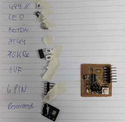
Just like in Eagle, I went through the library of components and this time laid them out physically. It was a lot easier this time as I had done it before in Week 4.
|
|
In between components I would use a Voltmeter to test pathways and make sure there were only desired connections making contact.
I decided to put the pins through the board and have the pins on the bottom because it would be easier for them to stay attached to the board.
This time took me only a few hours of soldering to make the board.
With my new board I plugged it in to our new AVRISP mkII (this tool is very useful for troubleshooting and identifying bad solders) and the light stayed red. I checked my connections and cleaned up any soldering that looked conspicuous. I tested paths with the voltmeter and after a few minutes of cleaning edges I had the light green.