Assignment:

Individual

-Make an in-circuit programmer by milling the PCB

-Optionally trying other processes

.ATtiny 45

.ATtiny 44


Group

-Characterize the specifications of your PCB production process.


Software :

-Fab mod

-Ubuntu OS


Materials :

-FR1 PCB board

-Soldering materials

-PCB components


Accomplised


-Successfully milled a PCB for ATtiny 45

-Soldered all components to the ATtiny 45 as per Brian’s design

-Uploaded firmware to make the ATtiny 45 to make it a programmer

-Worked on the group assignment to document the PCB milling process


Group Work


Before I begin explaining the whole process of milling and other assignments of this week I would like to talk about the basics of electronics first. When the lecture started this week all terminology used seemed like Greek and Latin. I did have to educate myself with the help of the internet and colleagues to understand what I was even expected to this week. I began by learning the very basics of electronics.


What is PCB?


One of the key concepts in electronics is the printed circuit board or PCB. It's so fundamental that people often forget to explain what a PCB is.Stands for "Printed Circuit Board." A PCB is a thin board made of fiberglass, composite epoxy, or other laminate material. Conductive pathways are etched or "printed" onto the board, connecting different components on the PCB, such as transistors, resistors, and integrated circuits.


PCBs are used in both desktop and laptop computers. They serve as the foundation for many internal computer components, such as video cards, controller cards, network interface cards, and expansion cards. These components all connect to the motherboard, which is also a printed circuit board.


Types of PCB


PCBs have copper tracks to connect the holes where the various components are located They are specially designed for each and every circuit and build construction very easy. Though, making the PCB necessitates special tools. The different types of printed circuit boards mainly include the following

1.Single Sided PCBs

This single sided printed circuit board includes just one layer of base material or substrate. One end of the substrate is coated with a thin layer of metal, usually copper because it is a good electrical conductor. Generally, a protecting solder mask be seated on the peak of the copper layer, and a last silkscreen coat may be applied to the top to mark elements of the board.

2.Double Sided PCBs

This type of PCBs is much more familiar than single-sided boards. Both sides of the board’s substrate include metal conductive layers, and elements attach to both sides as well. Holes in the PCB let circuits on a single side to attach to circuits on the other side.

3.Multilayer PCBs

These PCBs further enlarges the density and complexity of PCB designs by adding extra layers beyond the top & bottom layers seen in a configuration of double sided. With the accessibility of over many layers in multilayer printed circuit board configurations, multilayer PCBs let designers to make very thick and highly compound designs.

4.Rigid PCBs

In addition to having different numbers of layers & sides, Printed circuit boards can also come in changing inflexibilities. Most customers usually think of inflexible PCBs when they image a circuit board. Rigid printed circuit boards use a solid, rigid substrate material like fiberglass that remains the board from twisting. A motherboard within the tower of a computer is the best example of an inflexible PCB.

5.Flex PCBs

Generally, the substrate in a flexible board is a flexible plastic. This fundamental material permits the board to fit into forms that inflexible boards cannot & to turn or shift during use without harmful the circuits on the printed circuit board. Though flex boards tend to charge more to intend and create than rigid PCBs, they come with a number of advantages. For instance, they can restore heavy or bulky wiring in superior gear like satellites, where weight & space matter.

6.Rigid-Flex PCBs

Rigid flex boards merge technology from both flexible and rigid circuit boards.An easy rigid-flex boards comprises of a rigid circuit board that joints to a flex circuit board. These boards can be more compound if design requests demand.

PCB (Electronic)Components:


An electronic component is any basic discrete device or physical entity in an electronic system used to affect electrons or their associated fields.

If the copper traces behave like the skeleton of the PCB, acting as its basic structure – then the components are the vital organs. Each one has a different function. They give the circuit the unique qualities that make it fit for its intended purpose. Depending on the device or electronic item a PCB is designed for, different components will be needed for different circuits. These components can consist of a wide range of electronic parts. Before understanding the different type of components its necessary to know the type of technology they are goning to be used in. The technology is classified into two types as follows.

Surface-mount technology (SMT) is a method for producing electronic circuits in which the components are mounted or placed directly onto the surface of printed circuit boards (PCBs). An electronic device so made is called a surface-mount device (SMD). In the industry it has largely replaced the through-hole technology construction method of fitting components with wire leads into holes in the circuit board.

Both technologies can be used on the same board for components not suited to surface mounting such as large transformers and heat-sinked power semiconductors.

An SMT component is usually smaller than its through-hole counterpart because it has either smaller leads or no leads at all. It may have short pins or leads of various styles, flat contacts, a matrix of solder balls (BGAs), or terminations on the body of the component.

 Through-hole technology (tht), also spelled "thru-hole", refers to the mounting scheme used for electronic components that involves the use of leads on the components that are inserted into holes drilled in printed circuit boards (PCB) and soldered to pads on the opposite side either by manual assembly (hand placement) or by the use of automated insertion mount machines. Through-hole components are best used for high-reliability products that require stronger connections between layers. Whereas SMT components are secured only by solder on the surface of the board, through-hole component leads run through the board, allowing the components to withstand more environmental stress. This is why through-hole technology is commonly used in military and aerospace products that may experience extreme accelerations, collisions, or high temperatures.

Switch


Switches can come in many forms such as pushbutton, rocker, momentary and others.  Their basic function is to interrupt electric current by turning a circuit on or off.

Resistor


Resistors are used to resist the flow of current or to control the voltage in a circuit.  The amount of resistance that a resistor offers is measured in Ohms.  Most resistors have colored stripes on the outside and this code will tell you it’s value of resistance.  You can use a multimeter or Digikey’s resistor color code calculator to determine the value of a resistor.

Variable Resistor (Potentiometer)


A variable resistor is also known as a potentiometer.  These components can be found in devices such as a light dimmer or volume control for a radio.   When you turn the shaft of a potentiometer the resistance changes in the circuit.

Light-Dependent Resistor (LDR)


A light-dependent resistor is also a variable resistor but is controlled by the light versus turning a knob.  The resistance in the circuit changes with the intensity of the light.  These are often found in exterior lights that automatically turn on at dusk and off at dawn.

Capacitor


Capacitors store electricity and then discharges it back into the circuit when there is a drop in voltage.  A capacitor is like a rechargeable battery and can be charged and then discharged.  The value is measured in F (Farad), nano Farad (nF) or pico Farad (pF) range.

Diode


A diode allows electricity to flow in one direction and blocks it from flowing the opposite way.  The diode’s primary role is to route electricity from taking an unwanted path within the circuit.

Light-Emitting Diode (LED)


A light-emitting diode is like a standard diode in the fact that electrical current only flows in one direction.  The main difference is an LED will emit light when electricity flows through it.  Inside an LED there is an anode and cathode.  Current always flows from the anode (+) to the cathode (-) and never in the opposite direction.  The longer leg of the LED is the positive (anode) side.

Transistor


Transistor are tiny switches that turn a current on or off when triggered by an electric signal.  In addition to being a switch, it can also be used to amplify electronic signals.  A transistor is similar to a relay except with no moving parts.

Relay


A relay is an electrically operated switch that opens or closes when power is applied.  Inside a relay is an electromagnet which controls a mechanical switch.

Integrated Circuit (IC)


An integrated circuit is a circuit that's been reduced in size to fit inside a tiny chip.  This circuit contains electronic components like resistors and capacitors but on a much smaller scale.  Integrated circuits come in different variations such as 555 timers, voltage regulators, microcontrollers and many more.  Each pin on an IC is unique in terms of its function.

Schematic Diagram


When working with circuits, you will often find something called a schematic diagram.  These diagrams use symbols to illustrate what electronic components are used and where they’re placed in the circuit.  These symbols are graphic representations of the actual electronic components.

https://www.pcbtrain.co.uk/blog/the-basics-of-printed-circuit-boards-design-components-and-construction

https://www.makerspaces.com/basic-electronics/

Soldering


What is Solder?


Solder, as a word, can be used in two different ways. Solder, the noun, refers to the alloy (a substance composed of two or more metals) that typically comes as a long, thin wire in spools or tubes. Solder, the verb, means to join together two pieces of metal in what is called a solder joint. So, we solder with solder! The following link explains all about soldering right from types of materials to how to solder. It is a good read if you are a beginner like me.

Further, I watched a lot of videos on youtube to understand the soldering process and the art. Most of the tutorials are for Through hole components, but understanding the concept from that is the key.

What is the FabISP?


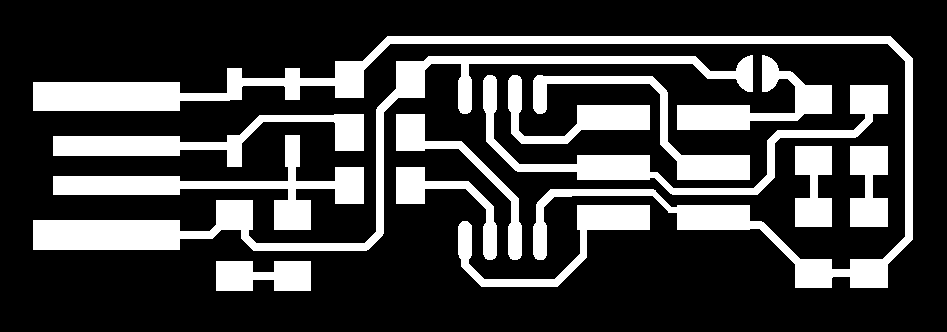
The FabISP is an in-system programmer for AVR microcontrollers, designed for production within a FabLab. It allows you to program the microcontrollers on other boards you make.

The Electronics Production assignment is to mill the board, stuff it with components and program it. We will be using these programmers through the semester to program the other boards we create.


As I understand the Basic FabISP has undergone many changes over the years by different people. The ISP namely ATtiny 44 and ATtiny 45 are named after their IC. I have used ATtiny 45 that was developed by BRIAN

PCB MILLING


Printed circuit board milling (also: isolation milling) is the process of removing areas of copper from a sheet of printed circuit board material to recreate the pads, signal traces, and structures according to patterns from a digital circuit board plan known as a layout file.

Source:

Wiki

In our lab, we have a Roland: Modela RDX-20. As I am using Brian's design for my ISP I downloaded the png from here:

http://fab.cba.mit.edu/classes/863.16/doc/projects/ftsmin/fts_mini_traces.png

http://fab.cba.mit.edu/classes/863.16/doc/projects/ftsmin/fts_mini_cut.png

As the group assignment was to characterize then PCB milling machine we tried and tested the parameters to trace and cut during our group work.


The Group Assignment can be viewed here


The software used here is FAB mod and it requires Ubuntu. Here is the step by step process to mill a PCB.


Note:

The milling process was to be done with fabmodules.org (Online version). But I have used the local version this week to mill my board. However in Week-7 I have milled my board using the online version. Please click here to redirect.


Step1.


Fire up the terminal in Ubuntu and type in fab

Opening the terminal

This should open another program asking for input and output process

Step2.


Fill in the appropriate input and out process. In my case png and Roland MDX-20

Make_png-rml

And then click on make_png_rml

Step3.


Fill in the appropriate input and out process. In my case png and Roland MDX-20

File Selection

On the top, the drop-down menu gives a few option like tracing or cutting and the milling bean size that is being used. In my case, I used a 1/64 mill

Parameters

Step4.


Fill in the other parameters to required numbers. I used an offset of 3.5 but later realized that it does not take in decimals but only whole numbers. Offset is basically the number of times the drill is going to cut from the traces. More the offset more time it takes to mill. Also, my speed setting was at 2 with the intensity at -0.05

Make Path

Step5.


Now before clicking on make rml I needed to prepare my board and milling bead accordingly.


I secured my board on the table with double-sided tape. Pressing the View button brings the plate forward so the board can be stuck or even used for inspection if any. At this stage, I set my milling bead a little higher than required.

View and Origin

Step6.


Pressing the view button again takes the tray inside and the bead aligns at the origin. Once this was done I moved the head to the origin my entering the coordinates in the software and clicking on move to xmin,ymin. In the origin was set I lowered the head on the board.

Adjusting the Milling bead

Step7.


The next step is to make rml. I made the rml file and began the milling process.

Milling

Milling

Note


Unfortunately, due to power problem, my milling stopped and I couldn't resume. So I had to mill again but this time with a slightly different parameter.

Re-Milling

Step8.


Once the milling is done press view to bring tray forward, inspect the cutting and clean the dust.

Re-Milling & Cleaning

Step9.


Now I changed the milling bead because I wanted to cut the board now. Once that is down load the png for cutting and check the parameter.

Changing head

Cut .png

Now, I used a 1/16 milling bead but the option available was for 1/32. So the parameters needed to be adjusted accordingly and this was tried during the group assignment. The thickness of the material as around 1.6mm but its always good to keep the cut depth a little lower than that. This was the tray won't get affected. Once the parameters are set click on make .rml. And begin milling

Cutting

Step10.


Once the milling s done press view and remove the board carefully. Make sure to leave the tray clean by removing excessive adhesives. This will help in keeping the tray flat as possible avoiding the bead from breaking.

Final PCB

Soldering


As I mentioned above soldering is an art. I went through tutorials on youtube to understand the good way to solder. I started off by collecting all the components required to solder.


Components list:

1x ATtiny45 or ATtiny85

2x 1kΩ resistors

2x 499Ω resistors

2x 49Ω resistors

2x 3.3v Zener diodes

1x red LED

1x green LED

1x 100nF capacitor

1x 2x3 pin header


As I said I used Brians design, so download the PCB layout and schematics from his site.

ATtiny 45 Layout

ATtiny 45  Scheme

I used the following tools to solder my board. The solder paste really helped to keep the iron tip clean. That produced neat solder.

Once I was set with everything I began the soldering process. It required really steady hands and a good amount of patients. The started off by messing the board while soldering.

After watching some tutorials and practice I came up with a system to solder.

1. Apply a bit of sodder to the board.

2.Reheat the sodder and using tweasers paste the component in position and allow to cool

3.once the component is in place solder the other side

Also once the solder in applied to the board, pull the solder and the iron in a quick motion. This leaves the board with a neat finish, like a concave surface. Removing it slowly creates sharp edges.

After Soldering

To my surprise, I did get the soldering right on the very first go. I was not a neat job but at least my connections were right and the connections did not overlap. This is how the ISP looked after completion. I used the multimeter to see if all my connections were intact. The results were positive.

These are  the two boards I soldered. Its far from perfect but its functional and I would definitely improve upon my soldering skills.

Checking and Programming the ISP


To start this process I installed Ubuntu LTS as a secondary OS.

https://www.ubuntu.com/download

Ubuntu can be downloaded from the above site.


Although Brian's site was clear on tutorial the begin process to install the AVR-GCC was confusing. After a few attempts with that method, I stumbled upon this site that explained well on Setting up AVR-GCC Toolchain on Linux.

http://maxembedded.com/2015/06/setting-up-avr-gcc-toolchain-on-linux-and-mac-os-x/

Followed this step by step instruction to install gcc-avr

The following are the commands used.

sudo apt-get update

sudo apt-get upgrade all

sudo apt-get install GCC-avr binutils-avr avr-libc

sudo apt-get install gdb-avr

sudo apt-get install avrdude

Installing gcc-avr

Once all the lib and avrdude is setup, its time to download the firmware.The firmware can be downloaded from the following link

http://fab.cba.mit.edu/classes/863.16/doc/projects/ftsmin/fts_firmware_bdm_v1.zip

I placed the downloaded firmware on my desktop and navigated to the desktop in the terminal with

cd ~/Desktop

Then unzip the firmware

unzip fts_firmware_bdm_v1.zip

I connected my ISP to the programmer. Plugged one end to the USB and the other on the header.


Green Light: means that the header is soldered correctly, the board is getting power.

Yellow Light: means that the board is getting power, but most likely the 6-pin programming header is not soldered correctly (re-flow your solder joints / check for cold joints, check for shorts).

Red Light: means that the board is not getting power - check for shorts.


And it was a delight to see the green light on the programmer. =D

Green on the programmer

Once this was done I navigated into the unzipped folder and entered the following command

make

This will build the hex file that will get programmed onto the ATtiny45.


The makefile needed to be edited. So I used gedit

Editing Makefile

What is usbtiny needs to be changed to avrisp2


Then I ran the following commands

make  flash

This will erase the target chip, and program its flash memory with the contents of the .hex file you built before.

make  fuses

This will set up all of the fuses except the one that disables the reset pin.

Running Fuse

Now to finally to check if the board works all the connections needs to be disconnected. Then I plugged in my ISP and ran the following command.


Lsusb


And the result should have "Multiple Vendors USBtiny" device.

NOTE: I had problems in this process with my other board. I checked my soldering and corrected that component that weren't soldered properly and then trying this command worked like a charm.!!

Checking USB

I was so excited to see that line in the terminal. My board finally works, meaning my soldering was correct and also the programming part.

Now, the last part is to disconnect the jumper.

De-Soldering the jumper

I plugged it into the USB again and ran


rstdisbl


This does the same thing as the make fuses command, but this time it's going to include that reset disable bit as well.

I then connected my ISP to Windows USB port to check if it recognizes it

Device manager

And Yes  !!!! It was displayed in the Device manager and in Control Panel as USBtinySPI

Finally, my programmer was ready. To check the ISP, I connected the programmed ISP to an unprogrammed one that I had soldered later as practice.

Connected Unprogrammed ISP with Programmed ISP

Watching that green LED glow was truly blissful..!!

Week 5 Group Work:


The assignment of the week was to characterize the machine. As all of us were new to the PCB milling and Modella, we as a group first tried to understand the machine and its parameters. We first went through the documentation of our previous batch to see how they had used the machine and what type of parameters they had used.

We also had the help of one of the students from campus who graduated FabAcademy last year. Chandni. She helped us figure out what parameters pertains to what kind of spindle movement. We experimented with different parameters and broke 2 nos. Of 1/64th drill bit in the process.

The whole process of how to operate the machine, using fab modules, changing the drill bit, what each parameters stands for etc, was a group learning process as all of us were new to using the machine.

Conclusion


This week started off in very alluring manner. I was fascinated at the same time terrified as all these new words were thrown at me. But as the week proceeded things slowly started falling into place and made sense to me. Milling and soldering is an art. I really enjoyed soldering and sometimes wished there was an UNDO button =D. I'm yet to master it though. The whole "programming the ISP "is still a little confusing, but I guess that will be clarified in the following weeks. On the whole there was a lot to learn and exploring this totally unexplored field for me was really exciting.


NOTE

The milling process was to be done with fabmodules.org (Online version). But I have used the local version this week to mill my board. However in Week-7 I have milled my board using the online version and also used Scarificial Layer. Please click here to redirect.

WEEK 5

This week is about electronic production. The basic intent of this week is to understand what a circuit is, the different types and components of a circuit board, milling a PCB and soldering. The lecture spoke about PCB fabrication process, types of PCB and components depending on the type of PCB. Then in depth, we were taught about soldering and its materials.


One of the key concepts in electronics is the printed circuit board or PCB. It's so fundamental that people often forget to explain what a PCB is.Stands for "Printed Circuit Board." A PCB is a thin board made of fiberglass, composite epoxy, or other laminate material. Conductive pathways are etched or "printed" onto the board, connecting different components on the PCB, such as transistors, resistors, and integrated circuits.

Surface-mount technology (SMT) is a method for producing electronic circuits in which the components are mounted or placed directly onto the surface of printed circuit boards (PCBs). An electronic device so made is called a surface-mount device (SMD). In the industry it has largely replaced the through-hole technology construction method of fitting components with wire leads into holes in the circuit board.

 Through-hole technology (tht), also spelled "thru-hole", refers to the mounting scheme used for electronic components that involves the use of leads on the components that are inserted into holes drilled in printed circuit boards (PCB) and soldered to pads on the opposite side either by manual assembly (hand placement) or by the use of automated insertion mount machines. Through-hole components are best used for high-reliability products that require stronger connections between layers. Whereas SMT components are secured only by solder on the surface of the board, through-hole component leads run through the board, allowing the components to withstand more environmental stress. This is why through-hole technology is commonly used in military and aerospace products that may experience extreme accelerations, collisions, or high temperatures.