Task:
GROUP assignment:
-
use the test equipment in your lab to observe the operation of a microcontroller circuit board
INDIVIDUAL assignment:
- redraw the echo hello-world board
- add (at least) a button and LED (with current-limiting resistor)
- check the design rules, make it, and test it
- extra credit: simulate its operation
Use the test equipment in your lab to observe the operation of a microcontroller circuit board
INDIVIDUAL ASSIGNMENT:
BASIC OF ELECTRONICS
I start reading about the basics such as Ohm’s Law, Kirchhoff's current law, Kirchhoff's voltage law, input (push button) and output devices.
Basic of Electronics (Sparkfun)
DESIGN RULES
Before I start designing my own PCB, I also read about some PCB design rules. I find these links very useful.
EAGLE
EAGLE stands for Easily Applicable
Graphical Layout Editor. EAGLE is a scriptable electronic design automation (EDA) application with schematic capture, printed circuit board (PCB) layout, auto-router and computer-aided manufacturing (CAM) features.
Our instructors recommend that we start with EAGLE. We have already worked with Eagle for the Electronics Production assignment. It is also interesting that EAGLE and Fusion 360 can exchange information. You can pull changes into EAGLE or push these changes to Fusion 360 and render your project. For the first PCB layout I will use EAGLE.
INSTALL EAGLE ON LINUX
- You need to download and unzip the last version of EAGLE.
I install the free version which is limited to 2 schematic sheets, 2 signal layers and 80 cm² board area.
- Right-click on the unzipped folder and select Open in Terminal.
- Now you have to type “./eagle run” to start EAGLE. After a few seconds, the Control Panel of EAGLE will open.
- You can add a new project in the Control Panel of EAGLE.
If you want to change the directory for the projects, to go
>Control Panel >Options >Directories .
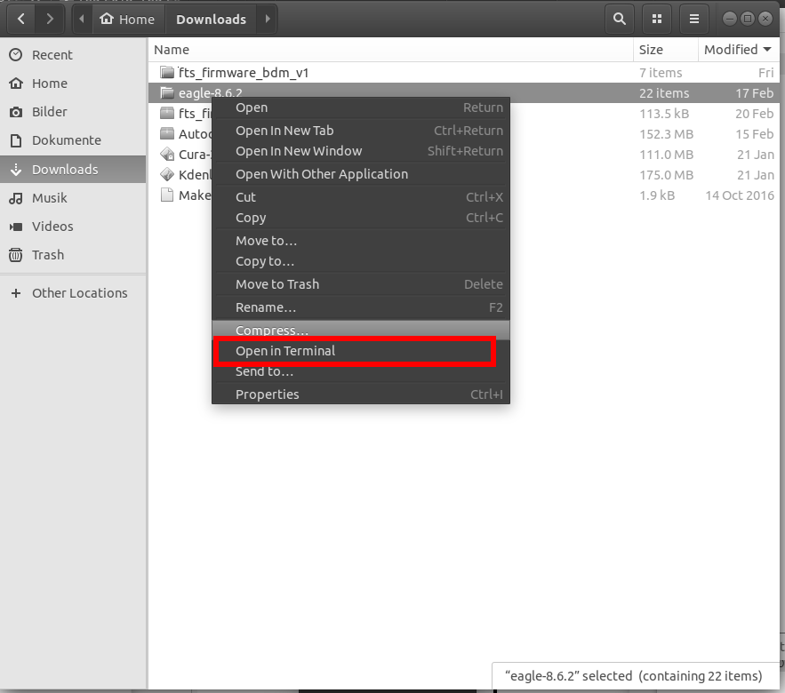 Openin terminal
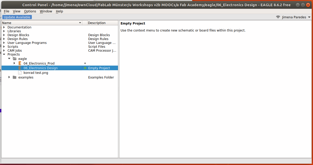 Control panel
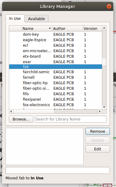 Add library
 SCHEMATIC VIEW
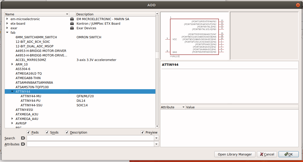
To start working with Eagle, I recommend reading the Fab Academy tutorial first. Then you have to download the fab.lbr file from the Fab Academy lecture page and start adding the components.
The next steps are to connect the components with the wire (“Net” tool in Eagle) and change the Grid Setting to mm.
It is also important to understand/read the fundamental schematic symbols. See the link above.
Link to How to read a Schematic (Sparkfun)
BOARD VIEW
Then I change the view to the board view to
route the traces between the components. The components are placed in no order and connected with yellow unrouted traces.
You have to 'Move' and 'Route' each component so that there are no shorts. I have chosen a width of 0.6 mm for the traces.
 Add components
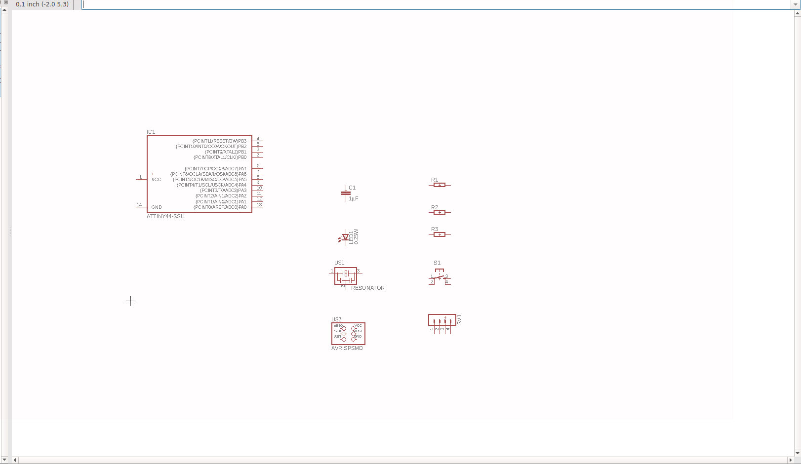 Schematic: Add components
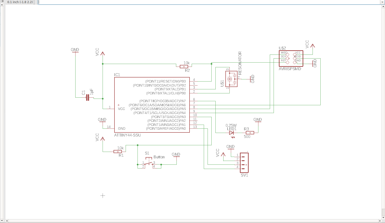 Schematic: Final version
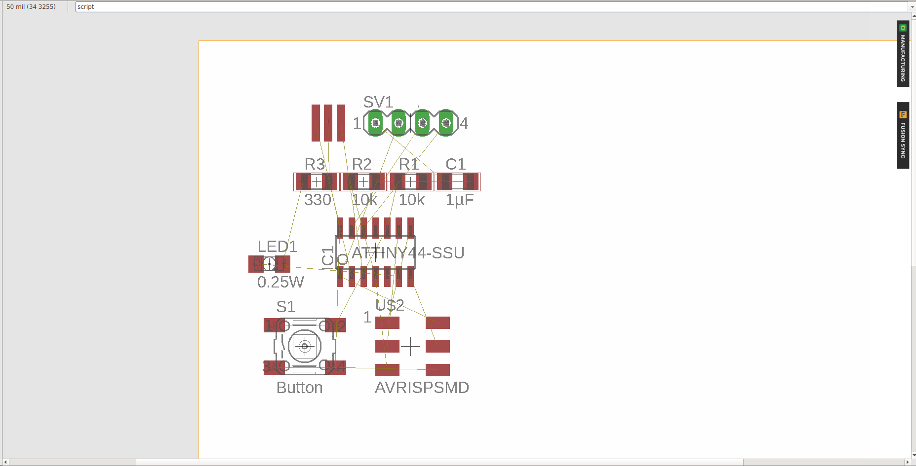 Board View
 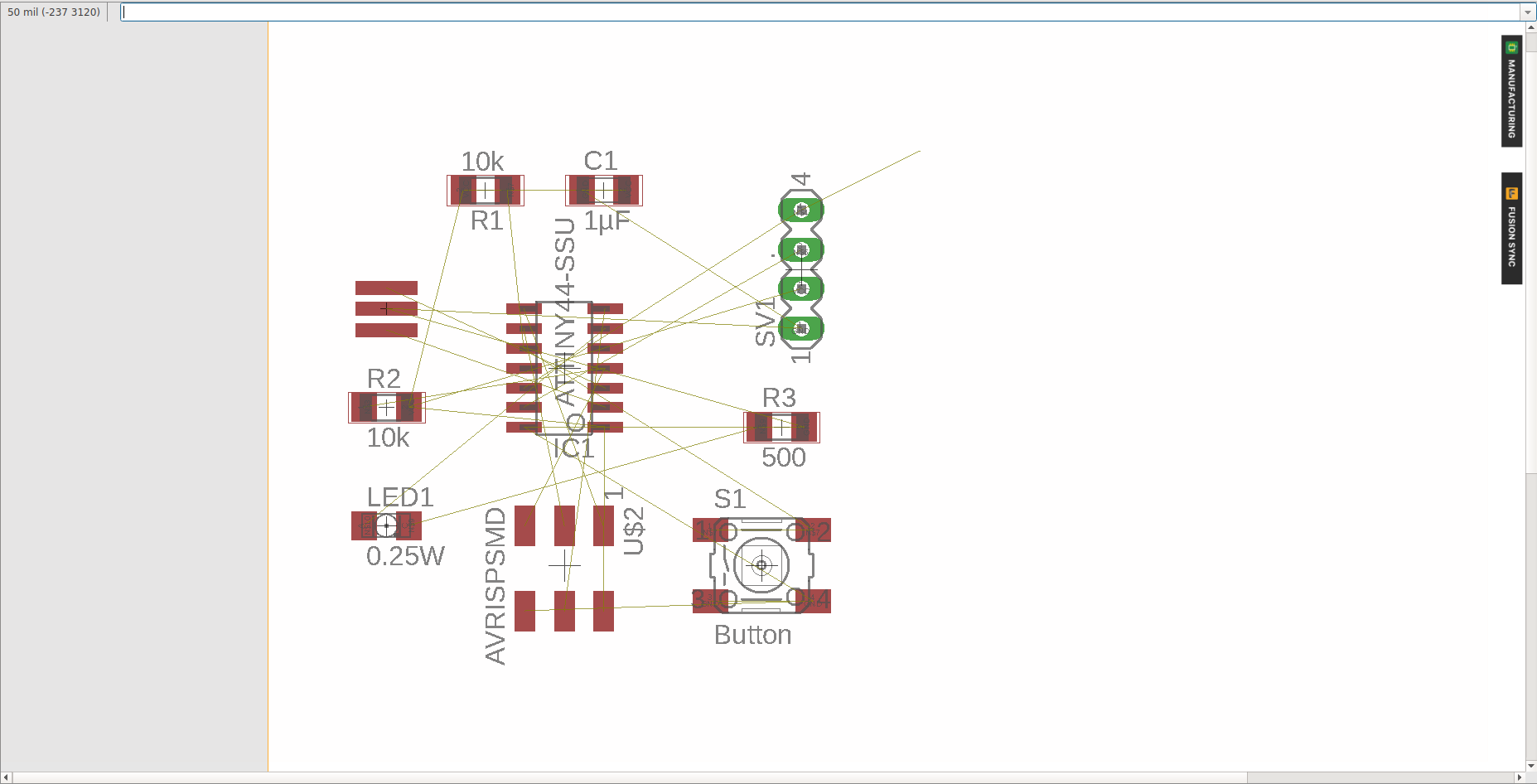 Board View, components moved
 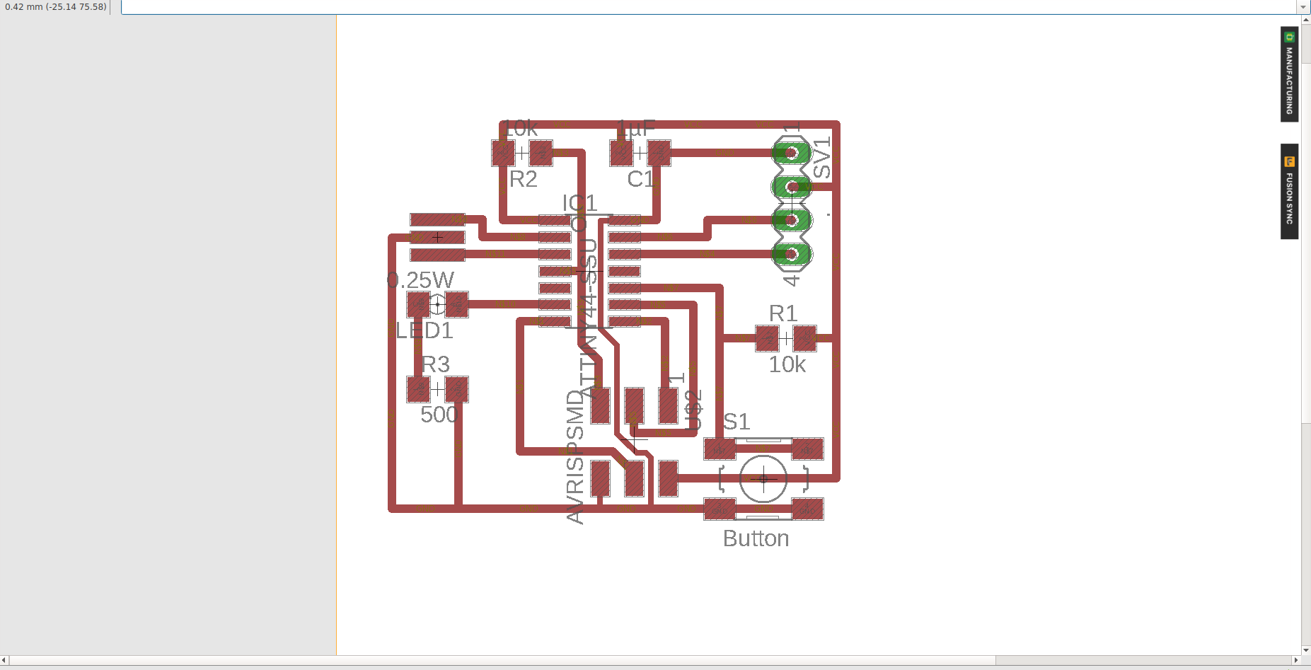 Board View, final version
DESIGN RULES CHECK (DRC)
First check the DRC-Settings, they must be compatible with the manufacturing technology you are using. To mill the board I use the Roland SRM-20 and the DRC settings from the Fab Academy tutorial.
The end mill I use for the traces and pads is 1/64 inch, and 1/32 inch for the outline.
DRC is used to check if the end mill goes between traces and pads. DRC also shows overlap errors. After moving some components and traces, the errors that DRC showed can be corrected. The settings for my layout can be found in the download section.
Note: Do not place the components too close to each other. You will need the space for soldering.
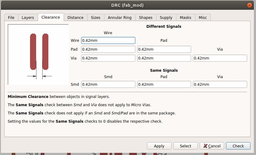 DRC
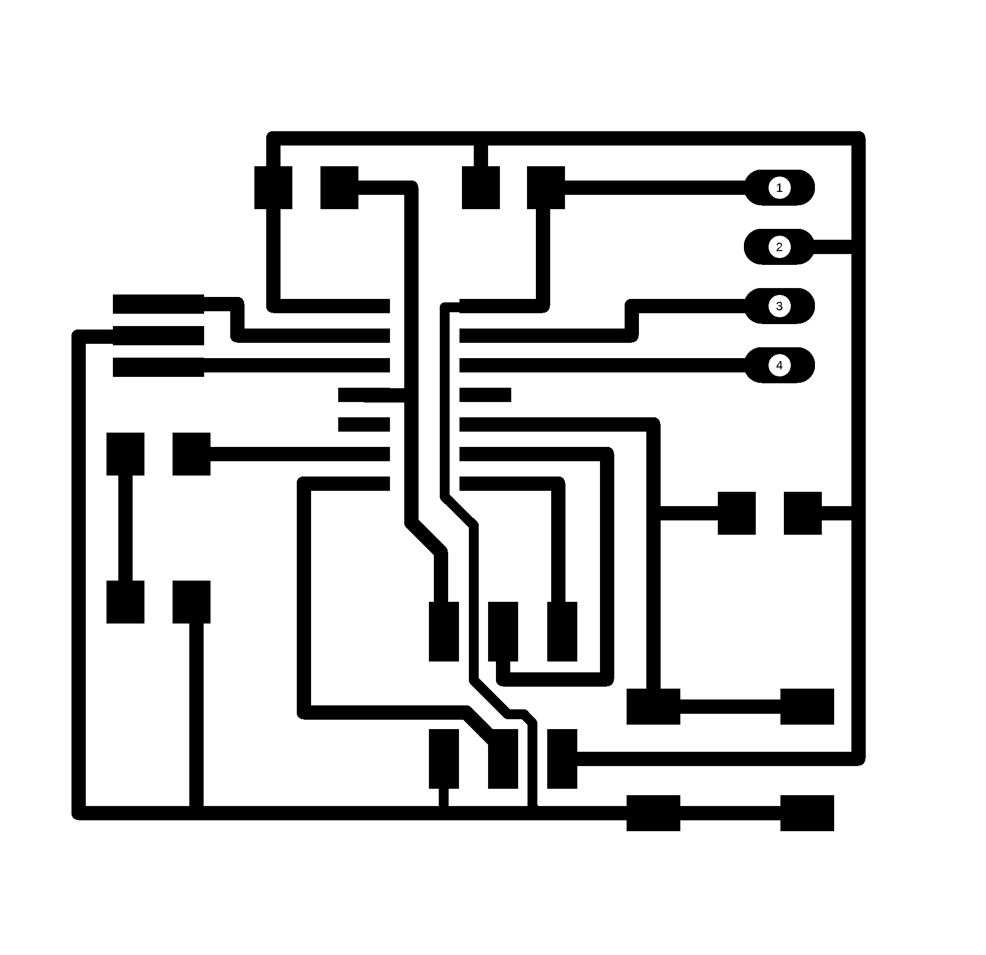
DRCEXPORTING THE DESIGN | GIMP
To export the layout as an image
file, you need to go to “Layer Settings” and select only the Top layer, you should see the traces and pads without text.
After that go to Export >Image >.PNG. The settings should be monochrome and 1200 dpi.
Note: the Roland CNC cuts out black and leaves white.
In Gimp, open the PNG file and follow these steps:
For the traces:
>Color >Value invert
For the outline:
> Rectangle select tool > Crtl + A
> Choose the color for the outline
> Edit > Stroke selection > 20 pix
> Crop Tool (to reduce the size of the image)
And export two PNG files (1x traces+pads for the 1/64 end mill and 1x outline for the 1/32 end mill)
 Eagle: export image
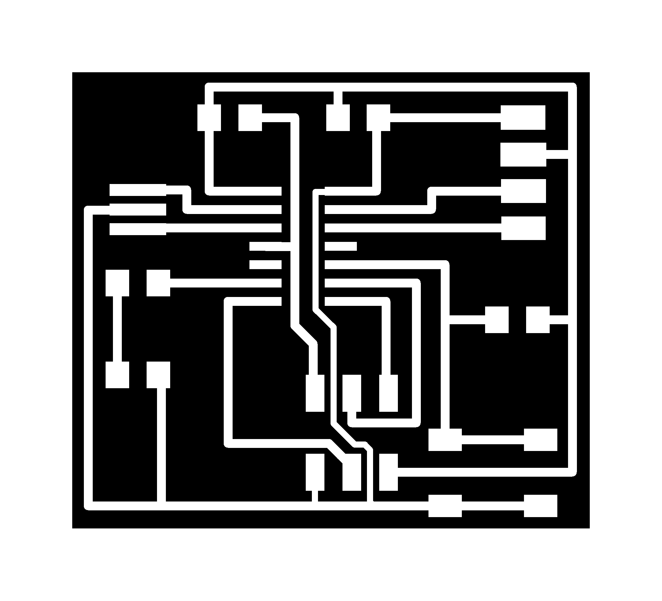 png file
MILLING THE BOARD
A) GENERATING THE MILLING PATH:
To generate the .rml file, I will work with the fabmodules. These are the settings I will use:
- Format (Roland mill .rml), Machine Output SRM-20, Process PCB traces 1/64 or outline 1/32.
- Set the home position x0:0 y0:0 z0:0, zjog 2mm and the end position x0:0 y0:0 z0:5 (this defines the end position after milling, it is important to set z-value above 0 mm. The end mill will not touch and damage the surface).
- Cut depth: 0.1 mm; calculate (to generate the milling path) and save the .rml file.
For the PCB I use this material:
- Base material is FR4 with a layer of thin copper foil (only one side). Thickness 1.6 mm.
B) SETTING UP THE MILL:
- Open the V-Panel for the Roland SRM-20.
- Click: view // for bringing the table in the right position to mount the board.
- Use double-sided adhesive tape between the PCB Blank and the sacrifice material and adjust both on the table of the mill.
- Insert the end mill into the collet and tighten the screw (don't use too much pressure).
- Set the home position in V-Panel by tapping the feed buttons for the X / Y / Z Axis (take care not to hit the PCB Blank) and use the different modes of the cursor step for fine adjusting. Let a bit of space in the Z-axis. The mill should not touch the board.
- Lose the screw at the collet to let the end mill drop carefully on the surface of the PCB-Blank at the home position.
- Tighten the screw on the collet to fix the end mill.
- Define the home position in V-Panel by clicking in X/Y and Z at the menu set the 'Origin Point' (use coordinate system must be set) // The XYZ values on the left side of the V-Panel window will turn to X: 0 Y:0 Z:0
- Start with 10% speed. Adjust the speed to 30%
- Start with 10% speed. Then adjust the speed to 100%
- Click 'Cut' to upload the .rml file.
- Click add and select the file
- To start the milling: click on Output
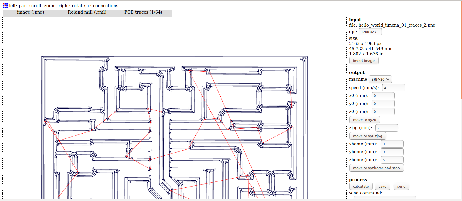 Fabmodules traces
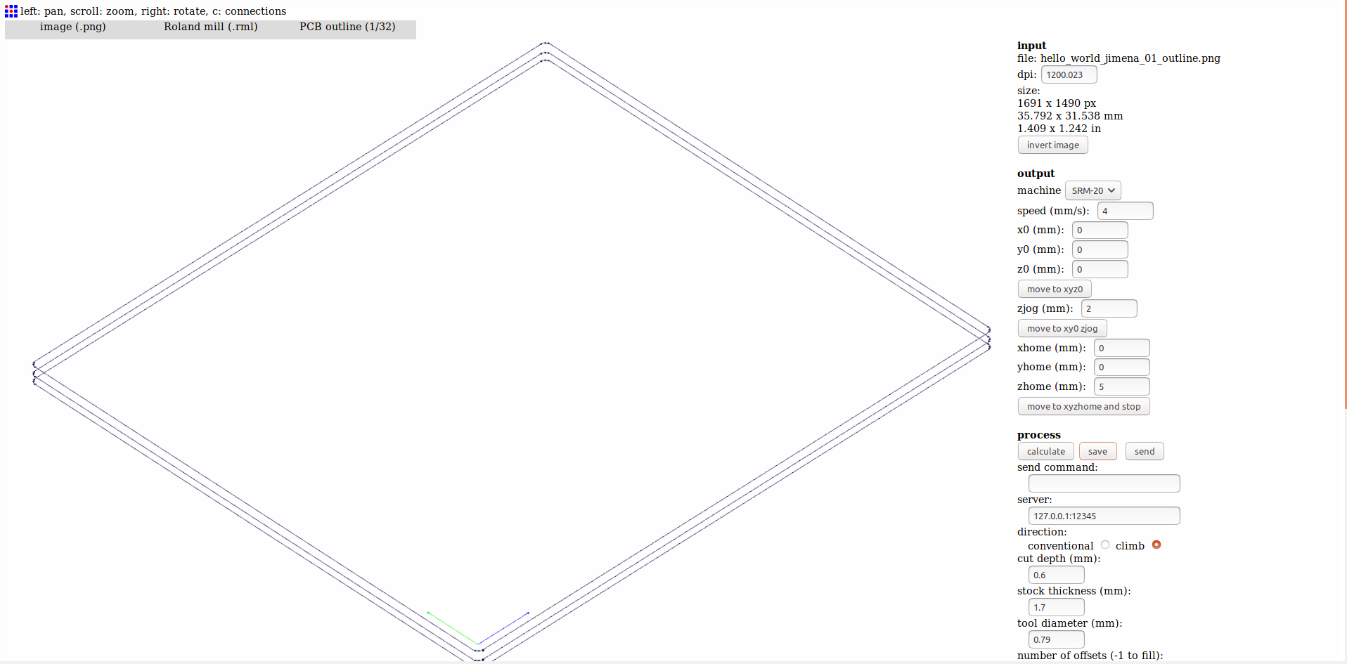 Fabmodules outline
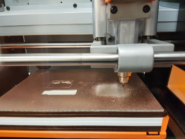 CNC
CNC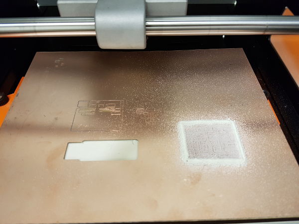 CNC
CNCSOLDERING
Before you start soldering, I recommend you to export the part list from Eagle and print out your board layout.
>Eagle Schematic >Export >Partlist
Check the size of the board and the footprint of the parts on your printout before you start soldering. More about this in “Group Assignment”.
Note: I find a short under the 6-pin header. Therefore I cannot program the board. I have to remove the pin header, check the copper surface and removed the short with a knife.
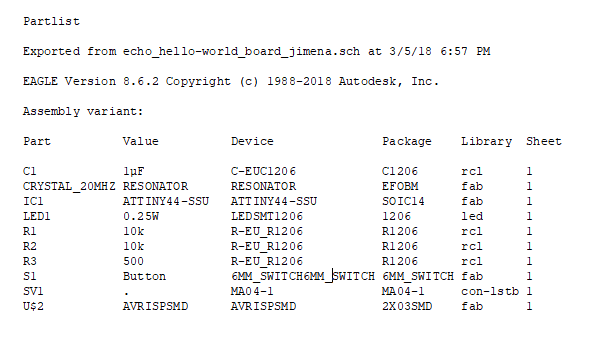 Partlist
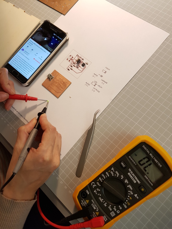 Tests with the multimeter
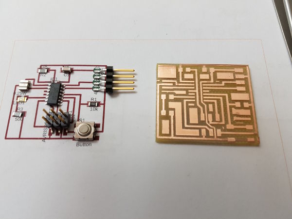 Components
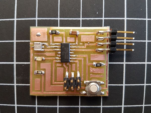 Hello-World board
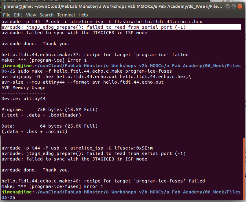 Shortcut on the board and error in the terminal
PROGRAMMING
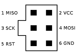
The first step is to connect the jumper on the board with the FTDI cable and the 6 pin header with the debugger to your computer.
I use the programmer Atmel ICE, see the link above.
It is important that you get pin 1 in the right place. Check the connectors graphic.
Then I apply this Fab Academy tutorial to program the Hello-World board, download the files and run the commands on the Ubuntu terminal:
→ $ make -f hello.ftdi.44.echo.c.make
(the files “hello.ftdi.44.echo.ot” and “hello.ftdi.44.echo.c.hex” are generated in the same folder.)
→ $ sudo make -f hello.ftdi.44.echo.c.make program-ice-fuses
→ $ sudo make -f hello-ftdi.44.echo.c.make program-ice
If you see several progress bars and no errors, it has worked.
Note: the file “hello.ftdi.44.echo.c.make” IS NOT complete. I have to add this text in the file to use the command in the terminal:
program-ice-fuses: $(PROJECT).hex
avrdude -p t44 -P usb -c atmelice_isp -U lfuse:w:0x5E:m
Check if Ubuntu finds the device with:
→ $ lsusb
 Atmel ICE connector
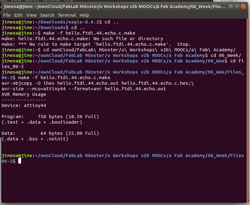 Programming
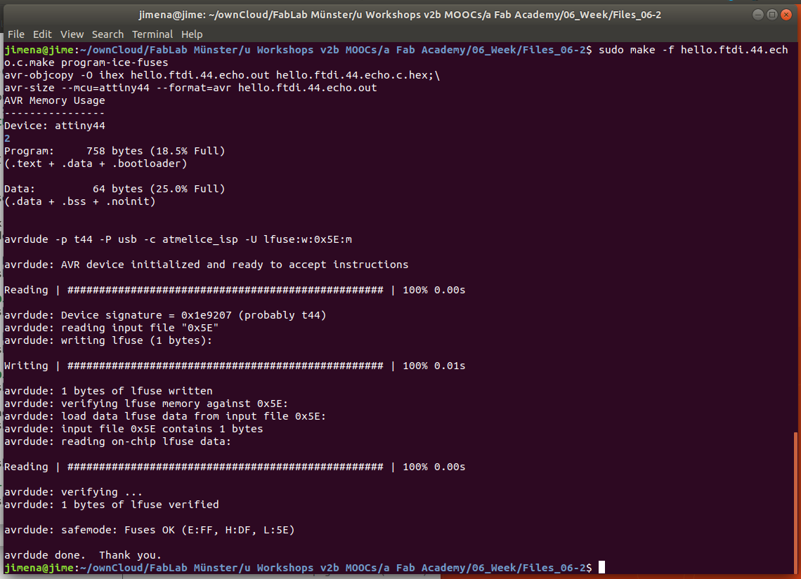 Programming
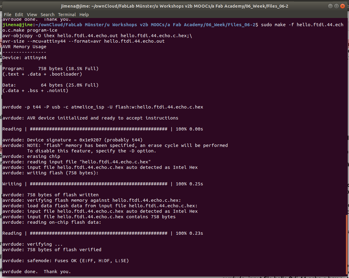 Programming
TESTING THE BOARD
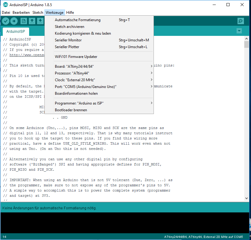
Note_Update: after installing an update for the Arduino IDE on Ubuntu, I can use the Arduino UNO as a programmer and burn the bootloader to the ATtiny44 without problems.
- First upload the sketch ArduinoISP on the Arduino UNO.
- Copy the following URL in the “Additional Board Manager”
https://raw.githubusercontent.com/damellis/attiny/ide-1.6.x-boards-manager/package_damellis_attiny_index.json
- and select the correct board: Attiny24/44/84 (more details on the screenshot).
- Select the programmer: ‘Arduino as ISP’ and then ‘Burn Bootloader’.
- Finally I can upload the sketch (screenshot) and test the LED on the board and the communication via the serial port.
 Burn Bootloader
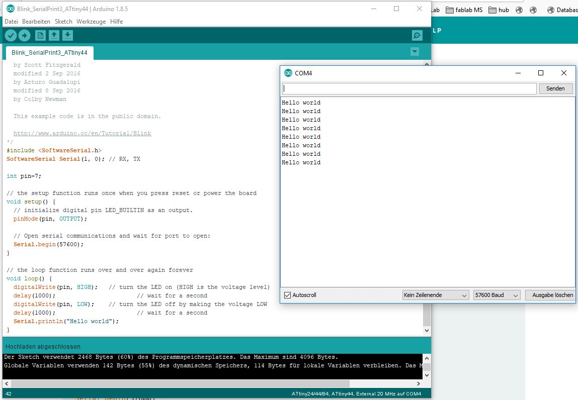 LED blinks | Serial Monitor
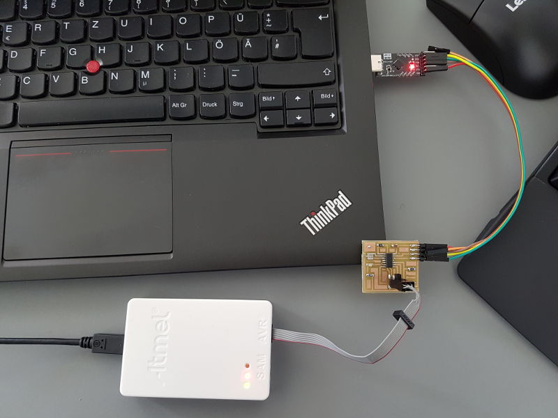 Board
BoardGROUP ASSIGNMENT:
USING THE MULTIMETER TO CHECK THE PCB
Continuity Test:
Test the continuity of the electrical traces with a multimeter. Turn the multimeter to the desired test function and verify that it works by touching the two probes (test leads) together. Most multimeters will beep or show “0” or a low value on the display. Place the probes on the connection, points and should hear a beep. If there is no connection, the display will show OL.
Check also each component, to make sure it is not damaged. For example the resistors with the:
Resistance Measurement:
Make sure the circuit under test is not powered on. The resulting current could damage the multimeter.
Chose the resistance measurement range: 200 Ω, 2 kΩ, 20 kΩ, 200 kΩ, 2 MΩ. Perhaps your multimeter has a different range.
Connect the black probe to COM and the red one to Ω. Take the resistor you want to measure and read the resistance with the test leads.
Measurements higher than 1 MΩ can take a couple of seconds.
Also read the manual of your multimeter for more information.
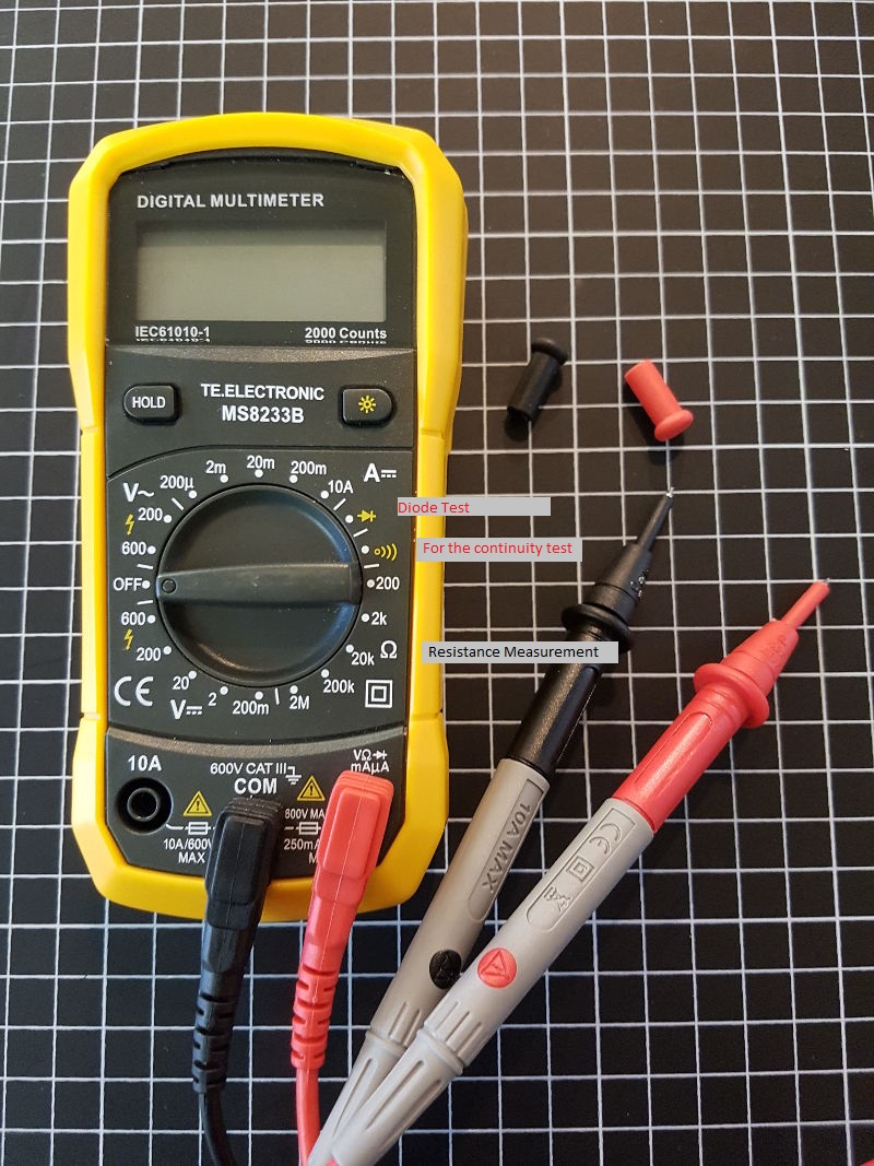 Multimeter
Download
| EAGLE files, DRC Settings and Partlist (zip) | Download |
| PNG and RML files(zip) | Download |