
Week 14
V-USB is a nice way to configure almost any chip into an USB1 device.
Compouter Networks, the book, seems like a nice read.
WireShark can be used for listening to a netweok.
Double Sided PCB
Since I want to make a Raspberry Pi HUT as a part of my final project, I will use the space of the documentation of this week to explore what has to be done in order to mill a double-sided board in the Fab Lab BCN environment.
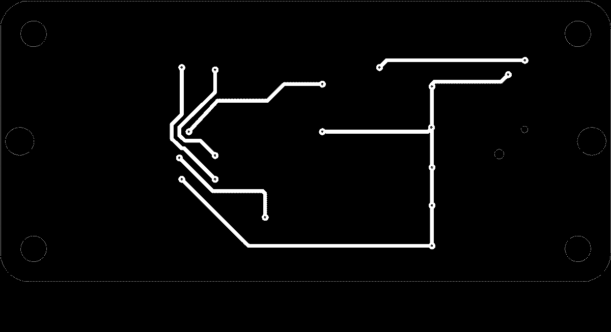
It starts with Eagle. Adding components, creating a schematic out of them. You arrive at a point where you can see parts connected and running ERC (Electronc Rules Check) shows you no errors.
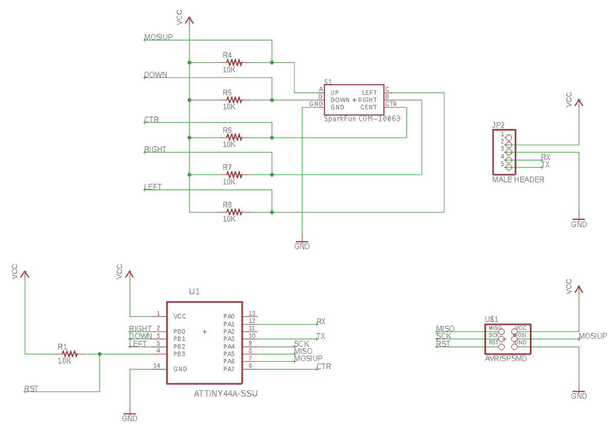
On the top part of the image you can see the SparkFun COM-10063 5-Way Tactile Switch component from the SparkFun Switches Eagle library. It is connected to the ATTiny44 component from the Atmel_By_element14 library by using pull-up resistors. That means ATTiny44 will read HIGH if the buttons are up and LOW if pressed.
There is an ISP header for programming the ATTiny44 and a header for connecting the HUT to the Raspberry Pi pins that will provide the board with voltage and do communication. The PA6 pin on the ATTiny is going to be used for both - programming the board and reading the UP button.
On the PCB side of the Eagle project, I started out by importing a DXF drawing to outline the dimensions of the board and guide the placement of the component pads. I made the DXF with Fusion 360, did a sketch with dimensions based on the Raspberry Pi Zero W designs and measurements found on-line; then exported by right-clicking the sketch layer and selecting the DXF export option.
I removed the previous dimensions and started to lay out the components. To create vias, one has to use the middle mouse button. What you do is you place a route and at some point when you need to place a via and continue the route on the bottom layer, you hit the middle button. The sequence of actions is as follows.
- Start placing a route on the top layer.
- Left-click to place a route on the top layer.
- Middle-click to tell Eagle you want a via.
- Left-click to confirm the via.
- Continue placing the route on the bottom layer (Eagle should switch the layer for you automatically)
- Repeat 3 and 4 to get back to top layer and finish the route.
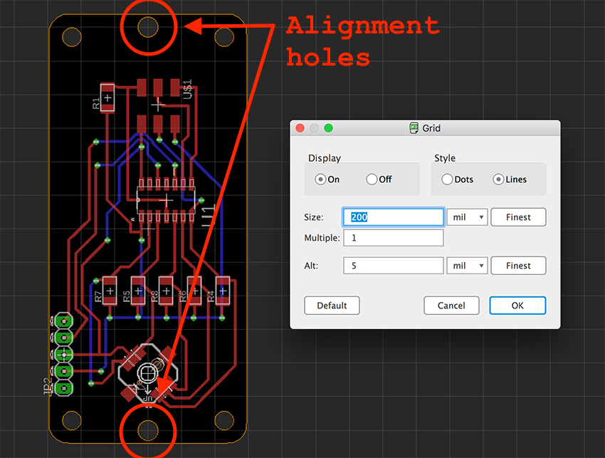
For the design rules, we have to know what is the size of the vias available at the Fab Lab BCN. For a double sided board we also need to know the size of the alignment holes.
- Vias: 0.4mm
- Alignment holes: 3mm
For the alignment holes I created two circles in Eagle layout on the Dimension layer. It took some time to figure out how to draw a circle with a specific diameter or radius. I found the following command that draws a circle with a radius of 1.5mm (3.0mm diameter) with the center of the circle being on the origin.
circle (0, 0) (1.5mm 0)
To move the circle into place and keeping the position along x axis the same, one has to do some manipulations with the grid. I set the grid size to 200mil (relatively big) and then I was able to move the circle from center to a position near the edge on the bottom and after drawing another circle, at the top of the PCB,
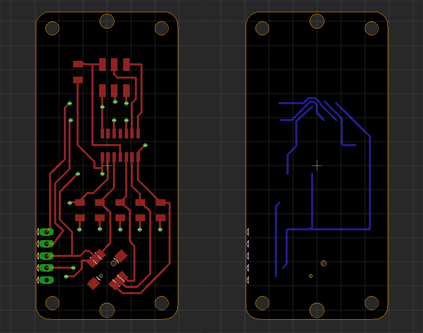
At this point I was ready to export the drawing as .png files. I need one .png image for each of the sides. For the top part I left the following layers visible.
- 1 Top
- 17 Pads
- 18 Vias
- 20 Dimension
For the bottom part, the following layers remained visible.
- 16 Bottom
- 20 Dimension
The settings to keep in mind while exporting (File / Export / Image) are the following.
- Monochrome: Yes (checked)
- Resolution: 500 dpi
- Area: Full
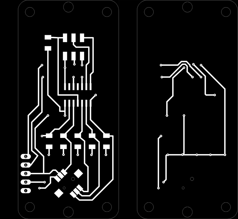
Now some Photoshop work. I start with opening the top, changing the color mode to RGB and importing the bottom part as another layer. I flip the bottom layer horizontally (Edit / Transform / Flip Horizontal). After doing the flip the alignment holes have to be aligned. In order to do that, make the top layer 50% transparent to see the alignment holes of the bottom layer.
Since I have a retina Mac, I had to change the resolution if the image in the Image / Image Size menu. I just want to change the resolution from 500dpi to 1000dpi in order to reduce the size in centimeters by two.
Make sure you unchech the Resample box in Image Resize dialog (only if you have retina Mac).
I made six strategies in total.
- 01-alignment (sacrifying layer only, 3.1mm bit)
- 02-holes (1⁄32 bit)
- 03-traces-top (1⁄64 bit)
- 04-vias (1⁄64 bit)
- 05-traces-bottom (1⁄64 bit)
- 06-outline (1⁄32 bit again)

Keep in mind that you have to use the File / Save As way of saving the .png’s in order to keep the dpi intact.
The interesting part in Mods was to configure the SRM-20 server program to use the 3.1mm drill bit for drilling the alignment pockets. In order for that to work I had to set the cut depth of the mill raster 2D module to 1⁄4 of the depth I wanted to get. I went for 5mm as the max depth which means 1.25 for the cut depth.
- tool diameter: 3.1mm
- cut depth 1.25mm
- max depth 5mm
For the rest of the passes the default mill traces and mill outline settings were fine. Except for the via pass I had to downscale the tool diameter.
Once I started milling I got worried about the jog height, is it high enough for the tool not to hit the alignment rods. The jog height was certainly not enough according to calculation. The rods would be a bit more than 3mm above the surface and the jog height for all the jobs was 2mm.
Then I realized that I can remove the rods once I have flipped the board and aligned it since it has double-sided tape holding it to the surface anyway. Thus I did not have to regenerate the toolpaths, but it would be much safer if one would set the jog height to at least 5mm.
Be smart and set the jog height in Mods SRM-20 module to 5mm (above the alignment rod overflow above the PCB surface).
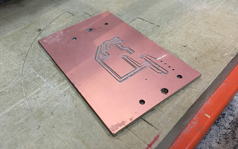
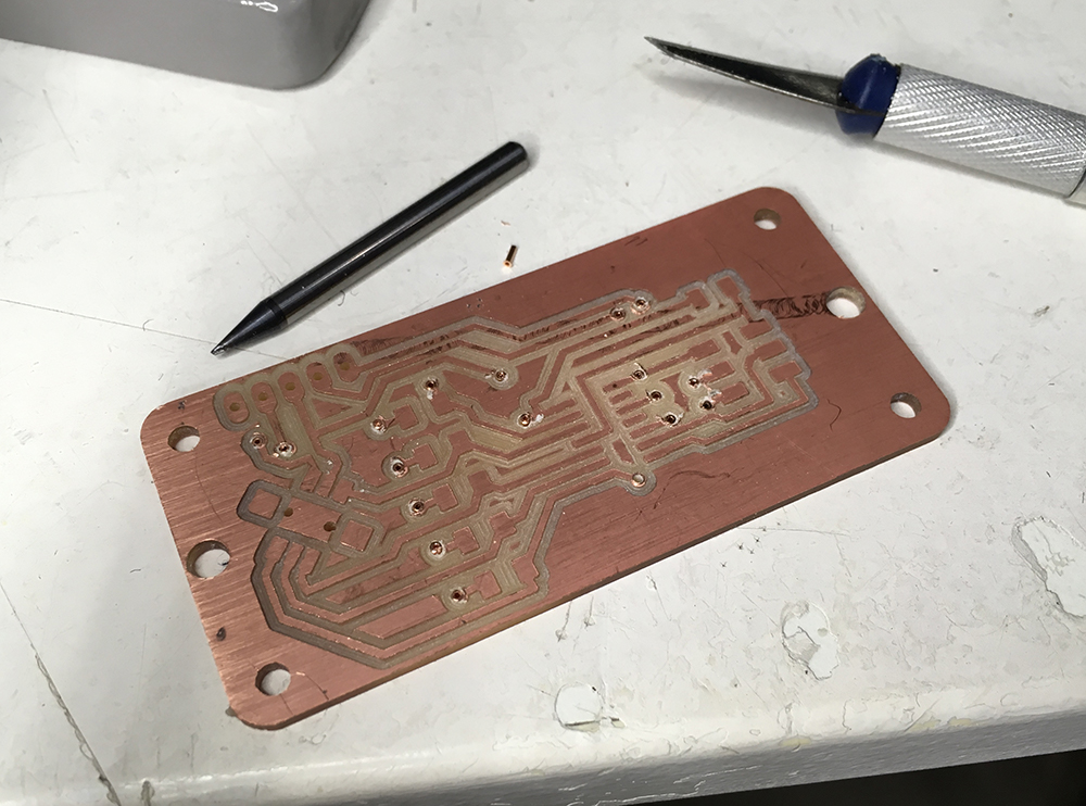
Milling iteration 01. While cutting the back side of the board, the job failed as the PCB started to move. It did that mainly because I did not use the alignment tabs.
This was also the opportunity to fix a few things in the design.
- Increase the pad size for the vias
- Fix alignment holes (since the previous ones were to small)
- Add more space (0.4mm) between the tactile switch pads
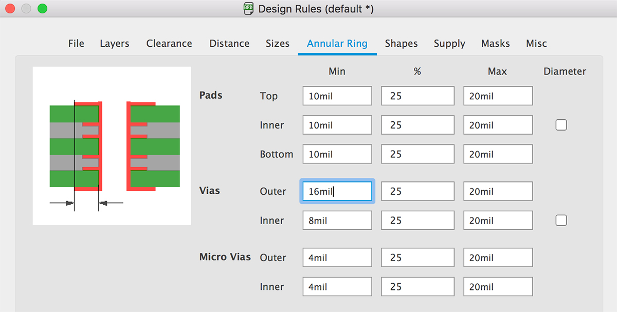
Increasing of the pad size can be done in Photoshop althought the proper way would be doing that in Eagle. The via pad size can affect the way the board is layed out, thus I chose to do that in Eagle. To adjust the via pad size in Eagle, go to Edit / Design Rules and click on the Annular Ring tab. Adjust the Vias / Outer parameter (I increased it from 8 to 16mil).
I had to adjust the routing a bit after, but not much. Next I would repeat all the steps from exporting .png images from Eagle and manipulating them in Photoshop.
In Mods, this time I made sure that I set the jog height high enough. I chose 10mm as the value.
Milling Iteration 02. While milling I discovered a weird behaviour at the end of the milling job. The Z axis was set to 0 and then X and Y axes were moved to 0, 0 thus leaving a scar on the surface. It was caused by a faulty GCode entry at the end of the file.
!PZ0,0
I changed that to the following.
!PZ0,1000
And it worked fine. As for the final result, the holes for vias were too small again and I had to use anything possible to make the holes bigger. That destroyed the copper layer and created connection errors after I placed the vias. Later I added solder on top of the via connections, but that destroyed the whole aesthetic.
Milling Iteration 03 was rather successful except the same problem with vias. Nonentheless I measured them again (0.5mm) and set the hole size in my design to 0.51mm, Mods and the milling machine did not create holes big enough.
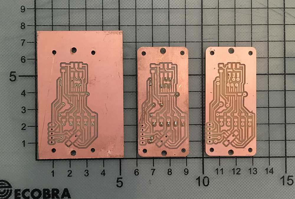
I had to use solder to support the via connections. Although I had a quick idea to check if any of the other holes on the board would be good enough for the vias. And I found one, it was made by the 0.8mm. I decided to make another iteration to make it right.
What I had to do was to move the top pocketing points that I made for vias to the hole drilling strategy and increase the diameter of the via holes to 8.4mm. I would skip the via pocketing step on the other side and improve the pin header clearance job (since it tried to pocket all the way through the board).
Milling Iteration 4 was the best so far and I managed to burn the bootloader and run basic test code.
There was one minor and one major issue to be solved before I could move forward with the network task to communicate between two boards.
- Power and debug LED’s would make things so much easier.
- Raspberry Pi GPIO serial expects
3.3Vcommunication, thus I had to integrate a voltage regulator in the PCB design. - I should add a place for vibration motor connection.
Also, since it is a part of the networking assignment, I should have two boards. Iteration 04 is good enough for sending commands (but using the Raspberry Pi only as a power supply). What I want to do is to have the new board receive them.
Logic Level Shifting
Next step was to integrate a logic level shifter into my design. After exploring the design of the SparkFun bi-directional logic level converter, I went to explore the Fab Lab BCN inventory to find the FairChild NDS355AN N-Channel Logic level Enhancement Mode Field Effect Transistor.
To better understand how it works I went on to consult the Wikipedia page on Field Effect Transistors. It has three terminals: Source, Drain and Gate.
Gate controls the conductivity between the Source and Drain terminals.
Source is where current enters the device.
Drain is where electrons leave the device.
I watched the following video to understand a bit more about MOSFET’s.
I watched another video to understand more about logic level converters in general. The following video explained it very well.
At this point I realized that to connect things to the RX pin of the Raspberry Pi I could use a simple voltage divider with a 10K and 20K resistor. To send a signal from the Raspberry Pi TX pin to the 5V driven ATTiny44 I would need to use a MOSFET-driven level shifter.
I had to look at another video to understand how it would work.
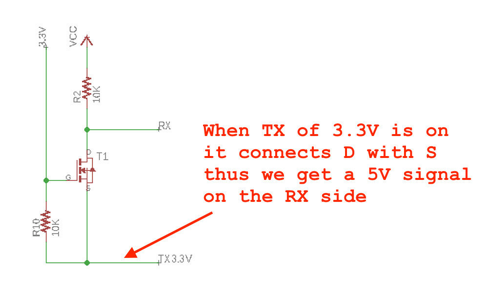
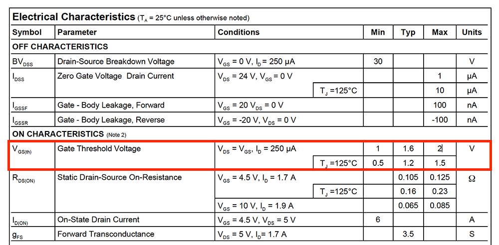
The good thing about this circuit is that it works both ways. I also checked the datasheet to make sure that 3.3V is enough to turn the gate on. I was looking for the Gate Threshold Voltage. The typical value is 1.6V which means the NDS355AN available at the lab is good to use for level shifting.
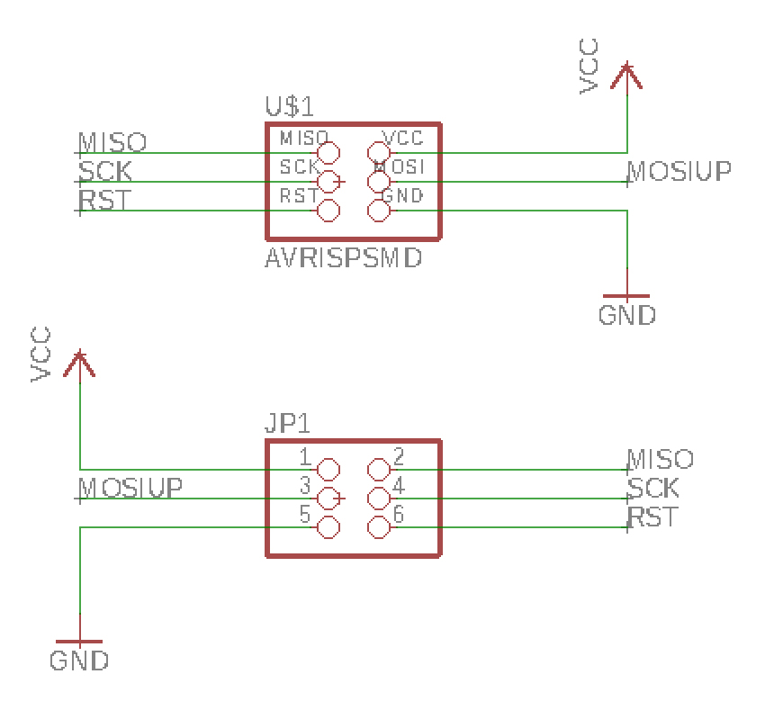
I moved on and integrated two level shifters in my circuit. It was much easier to integrate the LED’s and the motor connection. Another thing that I wanted to do is to use a 90deg ISP header so the ISP connector is on back side (the side facing towards the human holding the device). Below is an image showing the location.
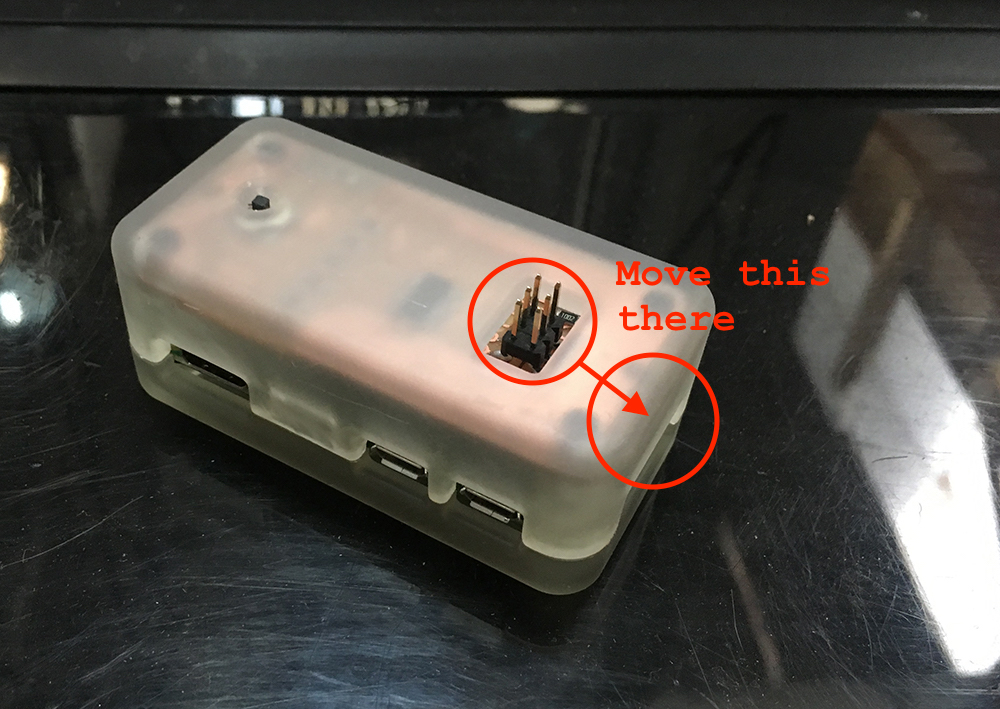
Since I will replace it with a through-hole pin header, I have to flip the connections.
Hardcore hacking mode happens here.
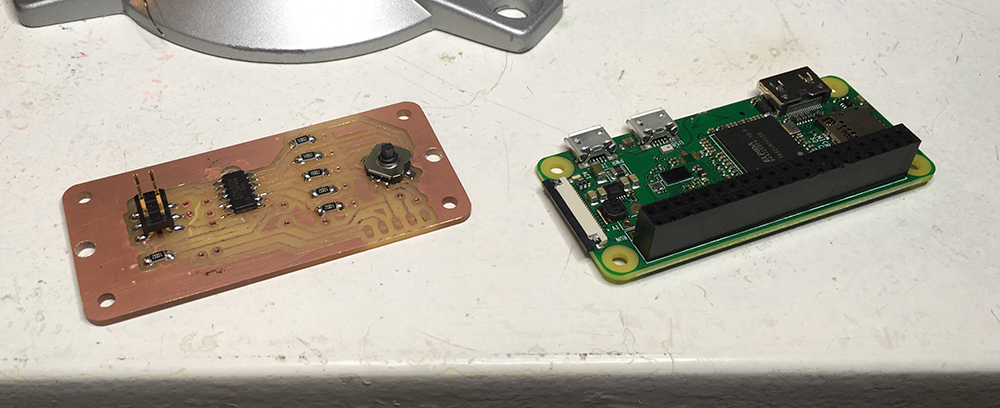
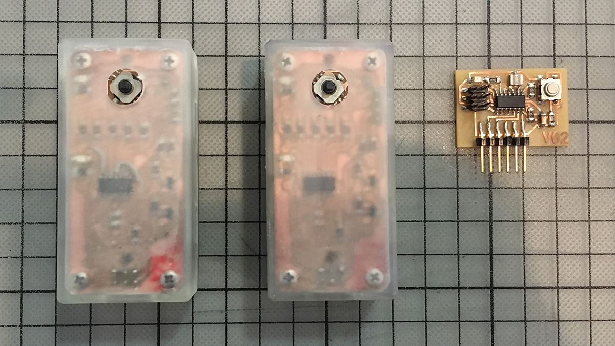
At the end of the process I ended up with two double-sided boards in a neat 3D-printed housing. As you can see I moved the ISP headers to the back side of the device.
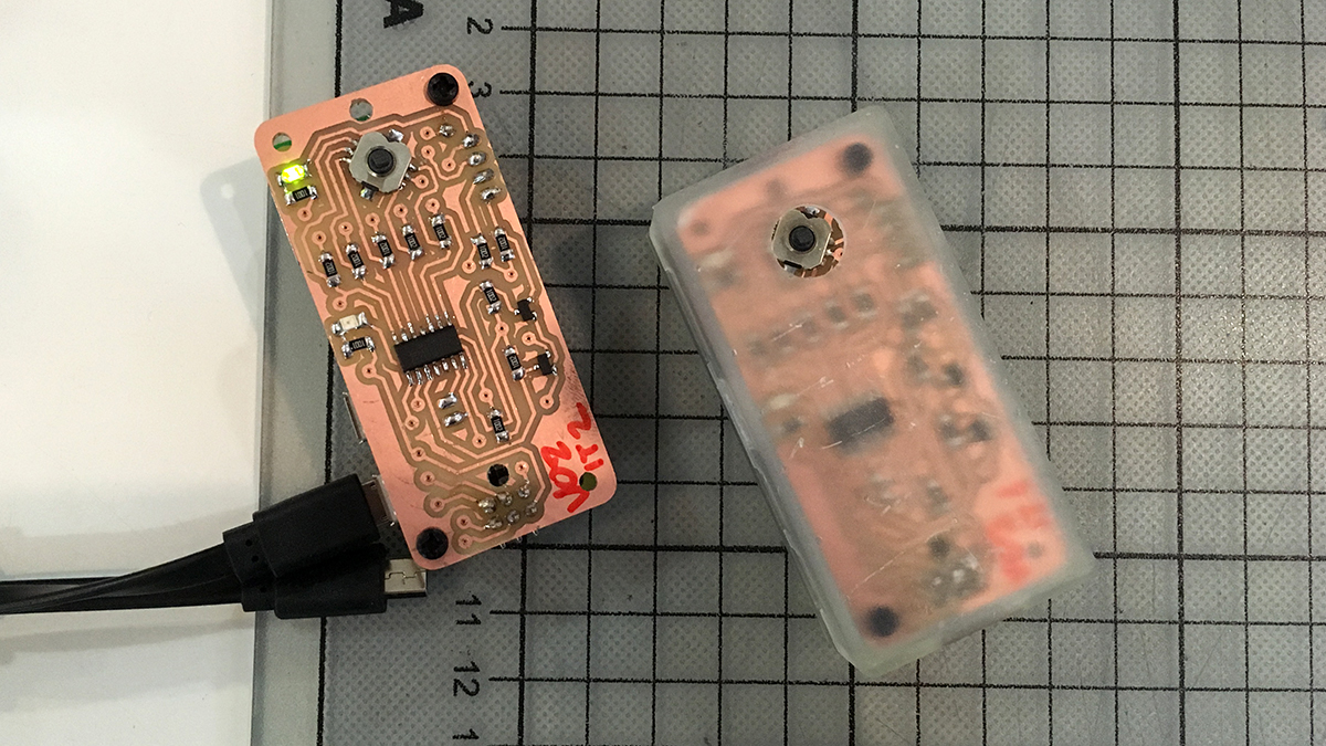
I also added a power status LED and a programmable LED for debugging. In order to program them, the Raspberry Pi has to be connected to power to provide 5V to the ATTiny44 sitting on the HAT board. Then a programmer can be connected to the ISP pins on the back side.
Networking
To demonstrate my networking skills I am going to make a little concert with the two devices and the Hello Board developed during the Electronics Design week. Since the two boards have vibration motors and programmable LED’s on them, one can make a real audiovisual show!
My plan is to make the Hello Board as a master device which contains the score. The two uMap devices will be slave devices, drive motors and blink lights. The score on the hello board will contain ON and OFF sequences for the vibration motor and LED of each board. I am going to trigger the sequence by pushing the button on the Hello Board.
I will power the Hello board using a FTDI cable from my computer. That will allow me also to send messages to the Hello Board through the serial connection. The plan is to forward these messages to all connected boards through an additional serial connection.
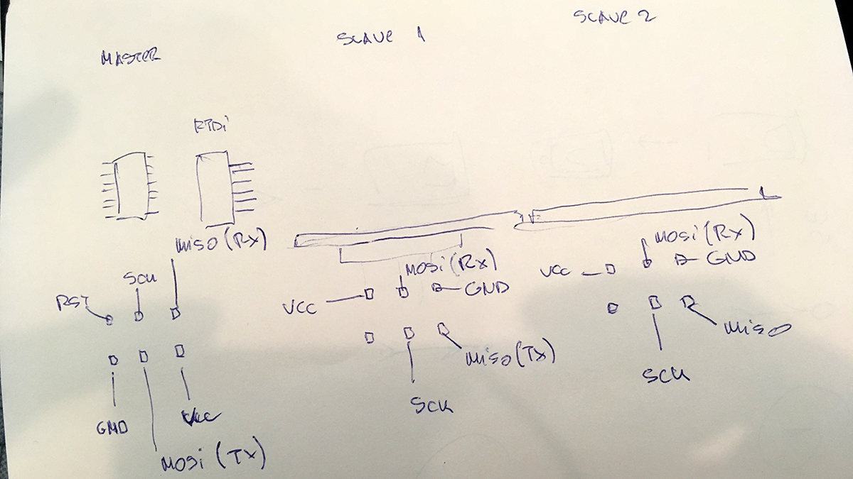
For that to work I had to configure two serial connections for the master board and one for each of the slave boards. To do that without error, I had to get an overview what connections I am going to use.
For the FTDI connection I used pins 0 and 1 of the ATTiny44 microcontroller. The fact that I used the same ATTiny for all three boards made things much easier.
#define FTDI_RX 0
#define FTDI_TX 1
I would use the second serial connection for forwarding the incoming messages and sending new ones. I would use the ISP connection for that since all of the boards have a connector and the layout of the pins is the same. For the master board second serial connection I would use pins 5 (MISO) and 6 (MOSI).
// Extra serial port on master
#define ISP_RX 5
#define ISP_TX 6
I would invert those on the slave devices.
// Receiving serial port on slave
#define ISP_RX 6
#define ISP_TX 5
I made a simple reference drawing for myself to identify the layout of the pins on each board to be able to connect the three-connector ribbon cable correctly.
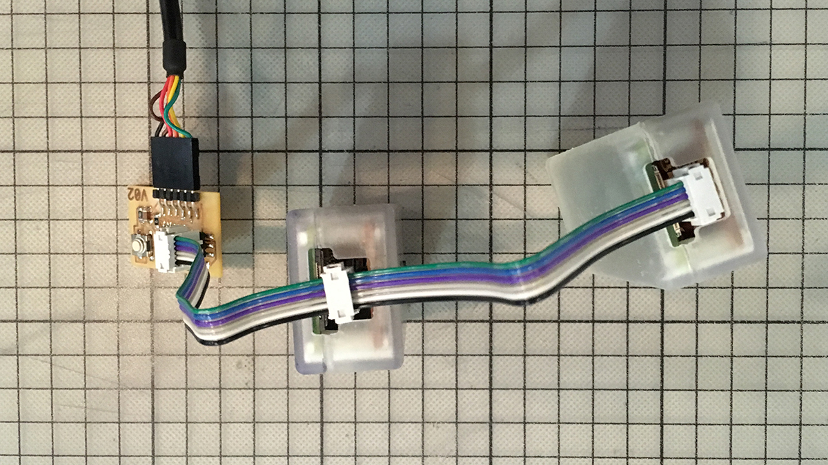
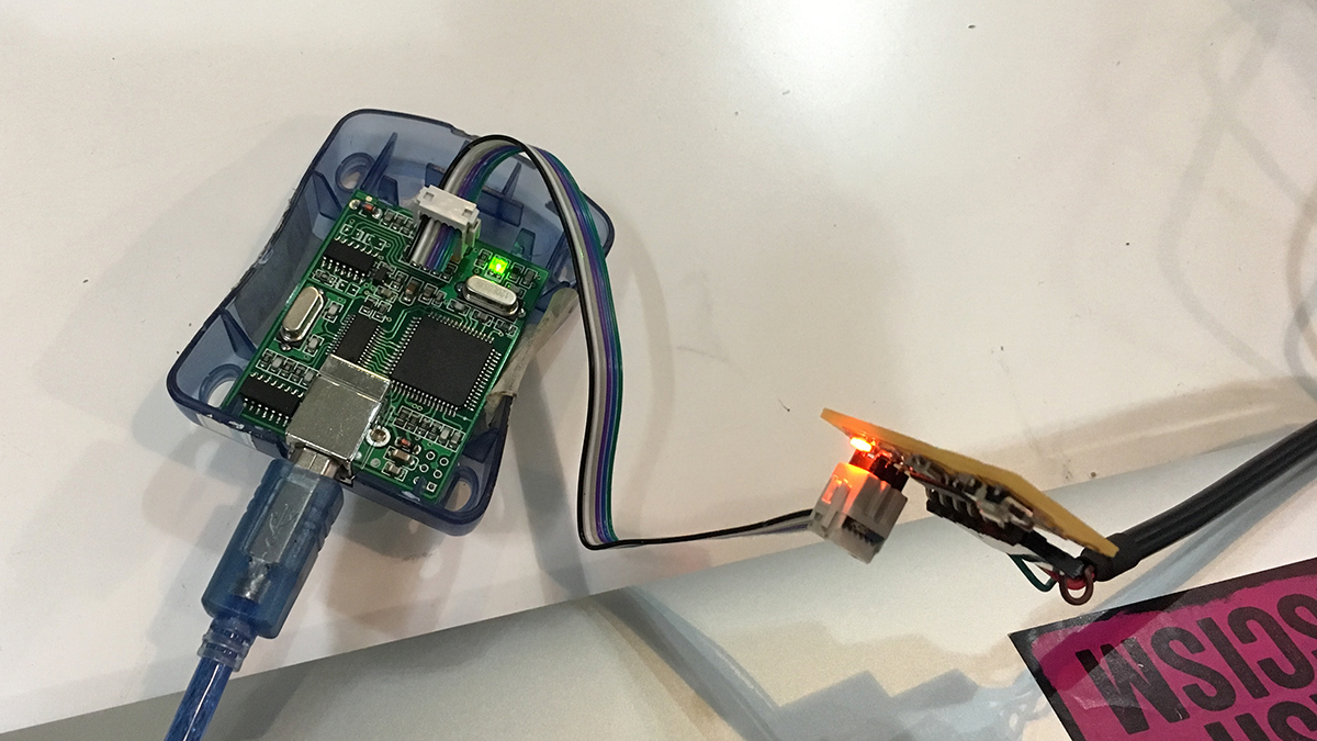
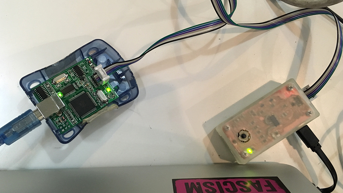
The following image shows a working connection between all devices. I use the ISP connectors also to power the other devices and as you can see my FTDI port gives enough power to drive all of them.
Next, the code part. I wrote two programs, one for the master, another one for the slave devices. For the slave devices I had to change the address variable before uploading it to each of the slave boards.
I did use plain serial with custom addressing protocol for communicating with individual boards. There are 3 elements in the protocol.
- Address: board
0or1 - Component: motor or LED (
0or1respectively) - State: ON or OFF (
0or1)
Since we are using only 0 and 1, one byte should be enough to transfer an addressed message. I used knowledge acquired during Embedded Programming week to shift speciffic bits in a byte before sending it to the serial line.
I used four arrays to address the motors and LED’s on the slave boards.
int slave0motor[] = {0, 1, 1, 0, 1, 0, 1, 0};
int slave1motor[] = {1, 1, 0, 0, 1, 1, 0, 0};
int slave0led[] =   {1, 1, 0, 1, 1, 0, 0, 0};
int slave1led[] =   {1, 0, 1, 0, 1, 0, 1, 0};
As you can see, each of them has 8 positions. It is a sequencer with 8 notes for each track. I used the arrays to create individual bytes to be sent through the serial line.
byte s0d0 = 0b00000000;
if(slave0motor[currNote] > 0){
  s0d0 = ((1 << 5) | s0d0);
}else{
  s0d0 = (~(1 << 5) & s0d0);
}
serialOut.write(s0d0);
Above you can see that the first step is to create a byte s0d0 which represents a byte for the motor device (0) of the first slave (0). Thus the first bit of the byte is 0 as well as the second one.
Then we are setting the third byte (which is fifth from the right, this is why there is 1 << 5) to 1 or 0 depending if the current note for the score of the motor is 1 or 0. Below is another chunk of code for the next device.
byte s0d1 = 0b01000000;
if(slave0led[currNote] > 0){
  s0d1 = ((1 << 5) | s0d1);
}else{
  s0d1 = (~(1 << 5) & s0d1);
}
serialOut.write(s0d1);
Here you can see that the second byte is set to 1 in the byte s0d1 = 0b01000000; line.
On the slave part we have to decode those. I use Serial.read() to read the byte and then a few bit shifting tricks to read the bits I need.
while (serialIn.available() > 0) {
    byte inByte = serialIn.read();
    int slave = (inByte & (1 << 7)) >> 7;
    int device = (inByte & (1 << 6)) >> 6;
    int state = (inByte & (1 << 5)) >> 5;

    // Stop here if this message is not addressed to this slave ID
    if(slave != slaveID){
      continue;
    }
    ...
}
The way how bit shifting works I describe in greater detail in the Embedded Programming week. Here you can also see how I use the slave address variable to tell if I want to do something with the device and state variables. If the slave byte matches first slave device (0) or second (1), each of them does things depending on what the device and state variable are set to.
int pin;
if(device > 0){
  pin = LED_PIN;
}else{
  pin = MOTOR_PIN;
}

if(state > 0){
  digitalWrite(pin, HIGH);
}else{
  digitalWrite(pin, LOW);
}
Below you can see images of the programming process. For the slave devices I used internal 8MHz clocks, for the Hello Board I used 20MHz clock, since it was on the board since the Electronics Design week.
It did not work the first time. I did a few test iterations while building the code. I could read a book about the whole process, but it worked at the end and you can see the proof of it by watching the video below.
Conclusions
This was a fun week as I learned a lot while developing the double-sided PCB’s. The actual networking part was easy related to the one of making the double-sided PCB, but it was like that as I have done things with networking before.
My main interest when joining Fab Academy was to learn more electronics and this is what I was trying to do with most of the weeks where electronics was involved, including this week. Now that I have made a double-sided board, I want to try to make one with 4 layers.
As for networking I always wanted to try someting as simple as one-bit addressing. For more devices one could use two or three bits for communicating the address. I like the simplicity and transparency of serial communication. Sending one byte over network most of the times (in terms of art installations) is completely enough to get the message around.
I can also say that this week probably is the most important one for my final project hence the double-sided PCB. The next step after the electronics work done here was to design and 3D print a nice case for the device.