Electronics Design
Or: Eagle
starting from parts and getting a board
Design the board
Import the Fab library into Eagle, so that you have all the parts in your library that you probably have on your shelf. I added a button and an RGB LED to the hello world standard circuit.
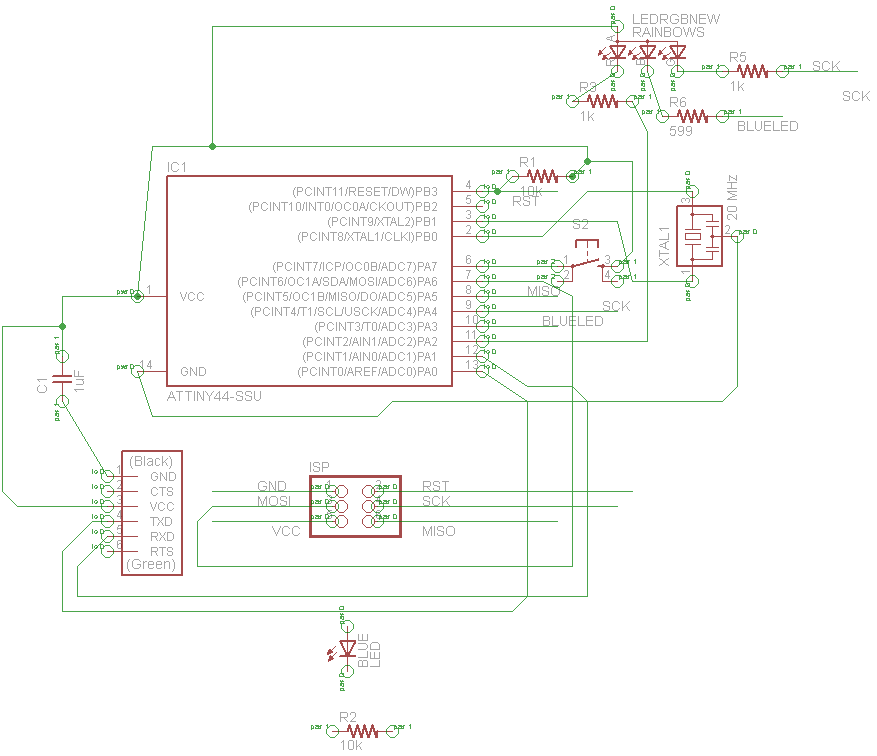
Nice example schematic
I learned a bit about how to lay out your circuit so it's easy to read. The most crucial advice was to not connect wires coming from headers. Instead, put them off to the side and label wires coming off each of them the same as the wires they connect to.
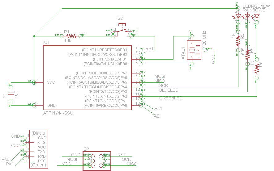
And now a terrible example schematic
When I first layed my board out it looked awful, which is why I asked around, and figured out some basic rules that turned it into the one above. Waterfall the resisters so their labels are easier to read. Don't wire up the headers, instead give their wires good names and name both sides. Wire the components near their pins.
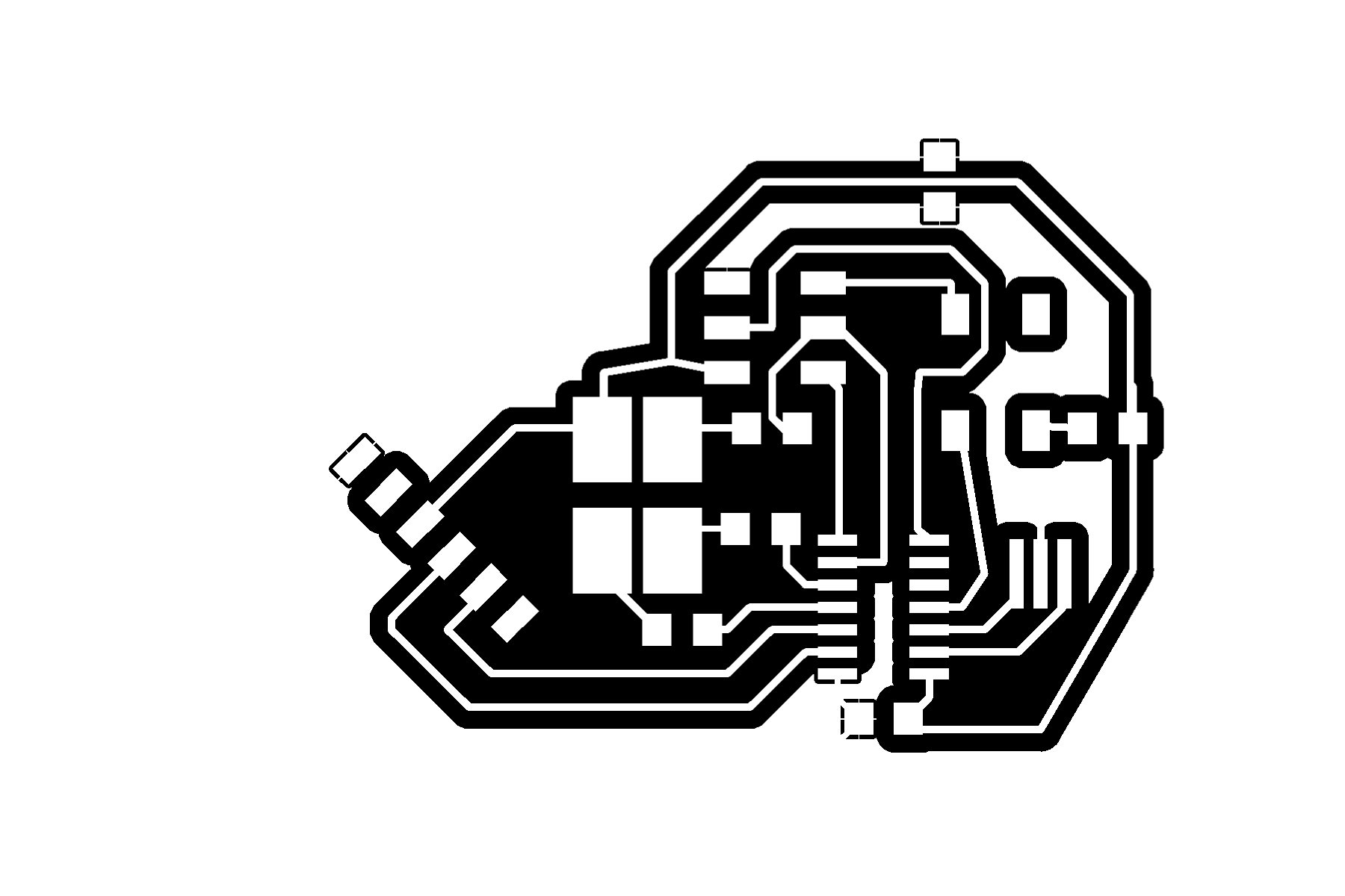
Board layout with a ground plane
exported and ready for cuting with the fab modules.
Edit the board for fun or… other design reasons
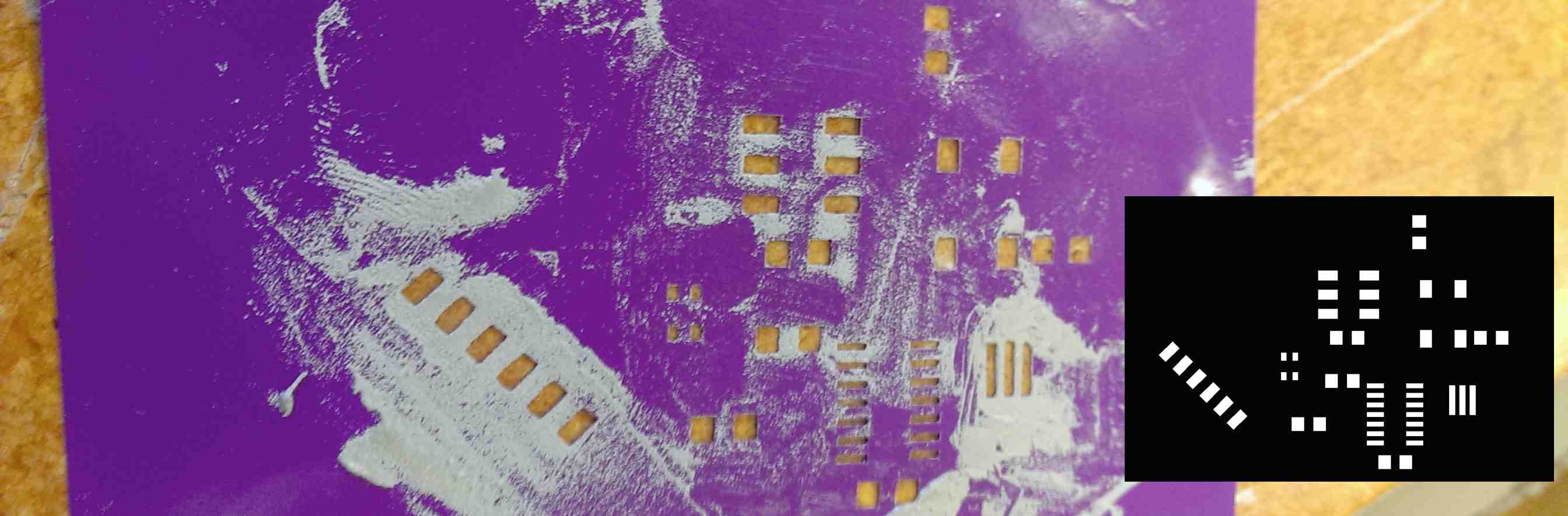
Export your board as an image (File, export, image, 600dpi Monochrome) and import into Inkscape. Odds are it will be the wrong size, unless all your settings align. Don’t worry, just resize it to the size you know it is. Make whatever shape you want the board to cut out as. Export two png’s (File, export bitmap, selection, 600dpi): one for the traces, one for the cutout

Cut your board
Just like two weeks ago, now we cut our boards on the Modela using the fab modules’ defaults for the 1/64” bit to mill the traces and the 1/32” for the cutout.
Cut and use your mask
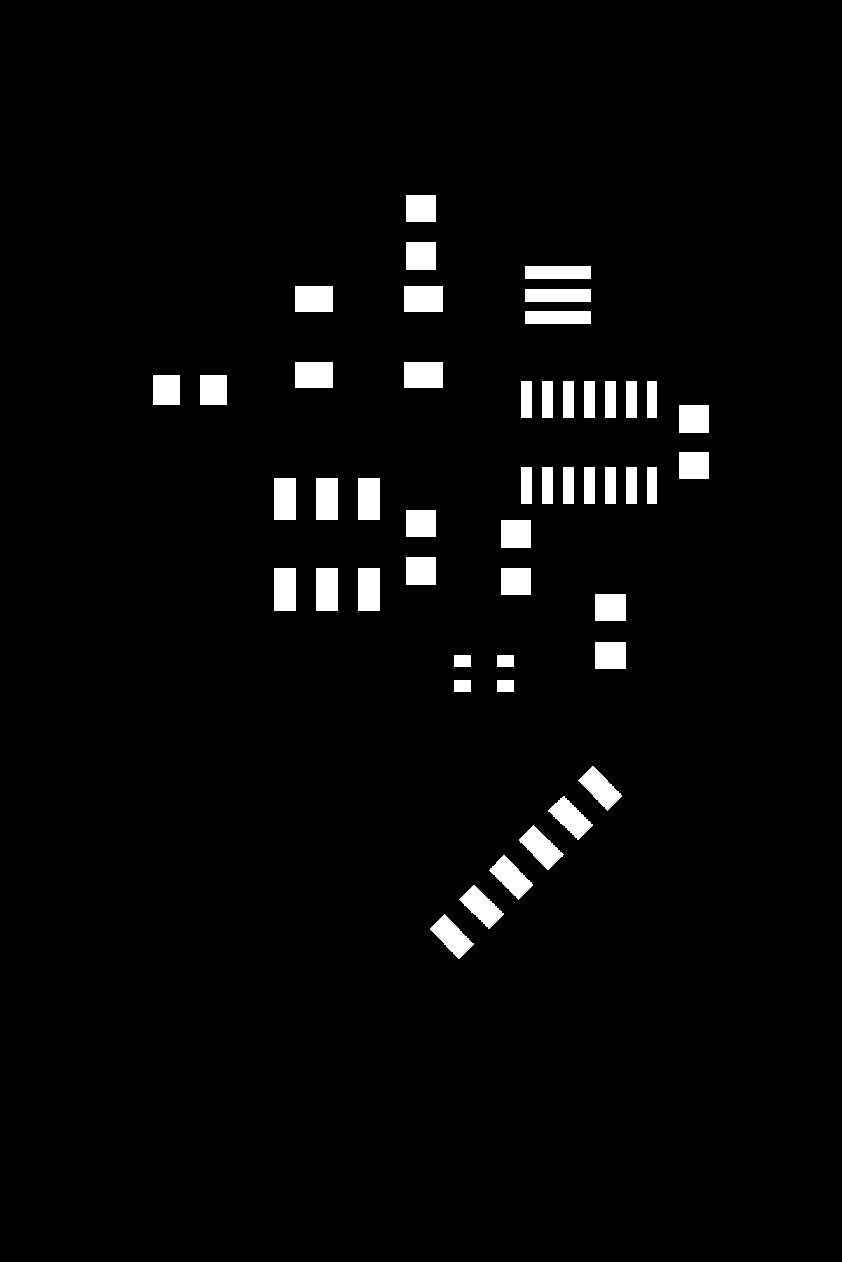
In eagle, export another image of just the pads. You can show just pads, or you can really fast ripup (type ripup; in the textbox at the top of the Eagle screen in the board window) all your traces, which leaves just the pads, then export that file (File, export, image, monochrome 600dpi). Take this and trace it in Silhouette. Be careful you know its size, because unless you have everything matching the size will be wrong. Trace it and cut out a vinyl sticker. Weed the sticker. Apply the sticker to the board. Put a tube/line of solder paste on one side and scrape a scrap board (or another flat sharpish, but not too sharp, object) across it to spread the paste evenly. If you don’t get all the pads the first time you can repeat till you’re satisfied. Finally, carefully take off the sticker you used as a solder mask.
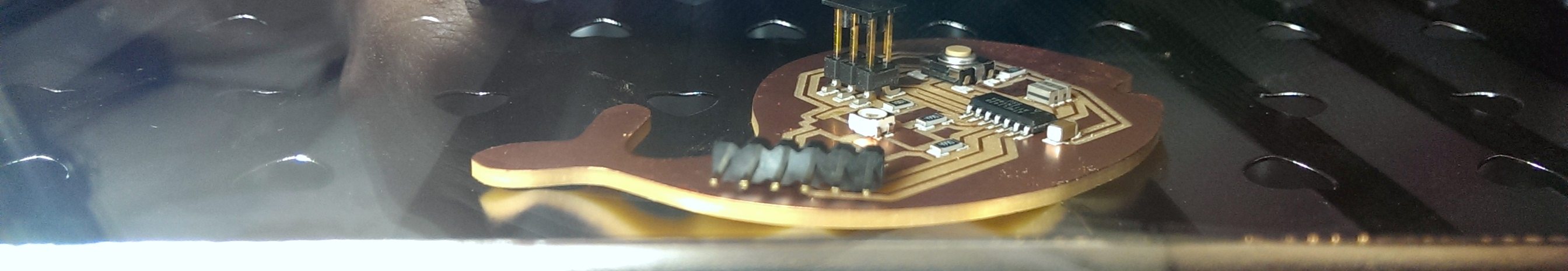
Populate and bake your board
Using your Eagle schematic as a guide, get out all the electronic parts you need for your boards. Place them on the pads that now have solder paste on them. Tweezers help.
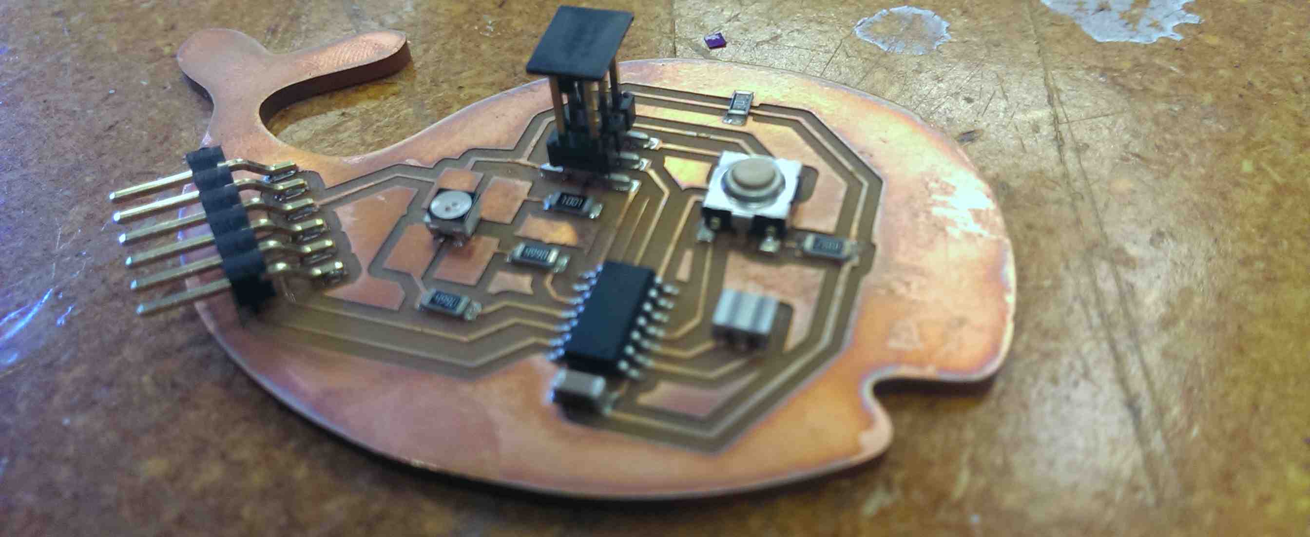
Theeen, you may have to jump in two places because you put the button in a really weird place. OK, now it's connecting things in a much less weird way. I disconnected the ISP RST pin from the button. Jumped that RST pin to pin 4 on the ATTINY44. Removed the resistor from between the button and VCC. And jumped the other, now disconnected side of the button to pin 6 on the ATTINY44.
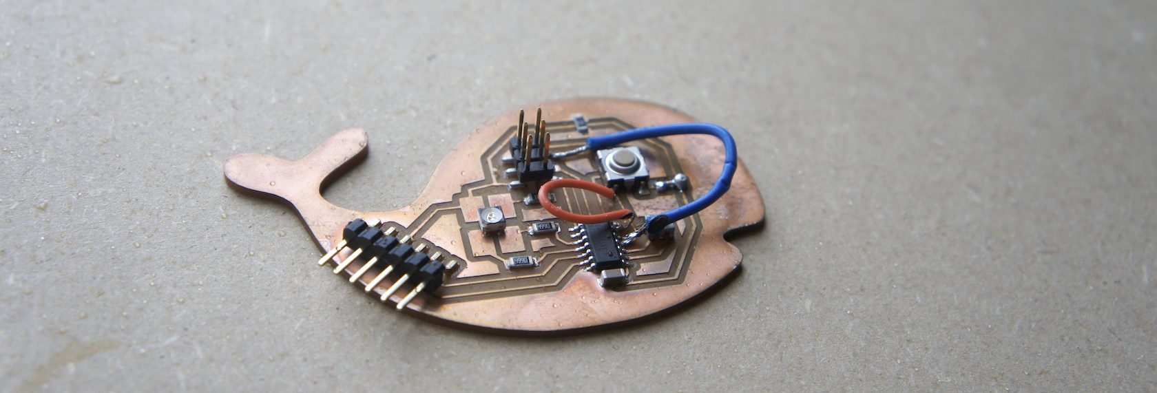
Program your board using the arduino IDE, according to the great directions on highlotech. To note! the pins on the ATtiny44 1-14 correspond to pins in the interface called VCC, pins 10, 9, RST, 8, 7, 6, and up the other side 5, 4, 3, 2, 1, 0, and GND. So, in this virtual arduino IDE coding universe, my LED connects to pins 2, 3, and SCK (4). The button is between VCC and pin 7. See next week for a description of the combined blinking/button code.
Downloadables:
The Fab library, EAGLE schematic and board design files. Also, the traces and cut image files for the fab modules on the Roland circut board milling machine, and the pads to cut from vinyl if you're using solder paste. Code described next week, together!