NODO

XIAO ESP32C3 + Fiber Laser PCB Manufacturing
This week focused on understanding the complete workflow of PCB fabrication, from the conceptual electronic design to the validation of a fully functional embedded system.
The main goal was not only to fabricate a PCB but to understand how fabrication parameters directly affect electrical performance. A 50W fiber laser machine was used as an alternative manufacturing method, replacing traditional CNC milling or chemical etching processes.
This required developing an understanding of digital manufacturing processes, thermal material behavior, and iterative experimentation.
The group assignment consisted of analyzing and characterizing the fabrication capabilities of a 50W fiber laser machine when applied to PCB production.
In this assignment, PCB fabrication will be explored using two complementary manufacturing technologies: CNC milling with a high-speed spindle and fiber laser machining. The goal is to compare precision, speed, and manufacturing constraints of each method.
.jpeg)
.jpeg)
.
View Week 08 Group Assignment.jpeg)
.jpeg)
Both technologies will be evaluated to determine their effectiveness in PCB fabrication, focusing on resolution, reliability, and workflow efficiency.
This section defines the minimum design constraints and fabrication rules for producing PCBs using two in-house technologies: CNC milling and JPT 90W fiber laser. These rules ensure manufacturability, reduce errors, and improve repeatability in the production process.
These rules define the baseline for PCB layout design before fabrication. Proper adherence ensures higher yield, reduced iteration cycles, and compatibility with both CNC and laser manufacturing workflows.
.jpeg)
.jpeg)
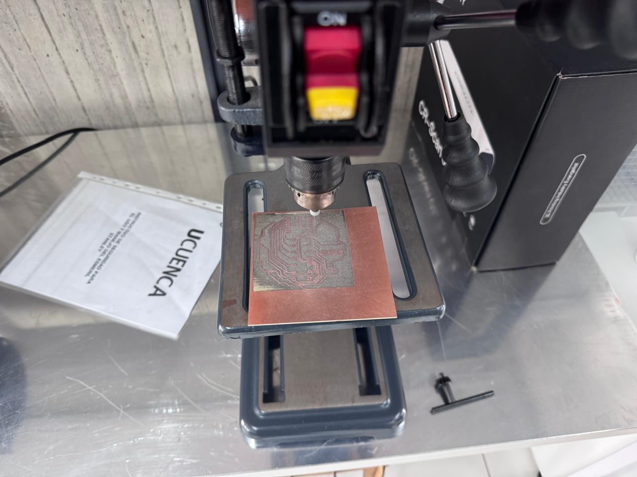
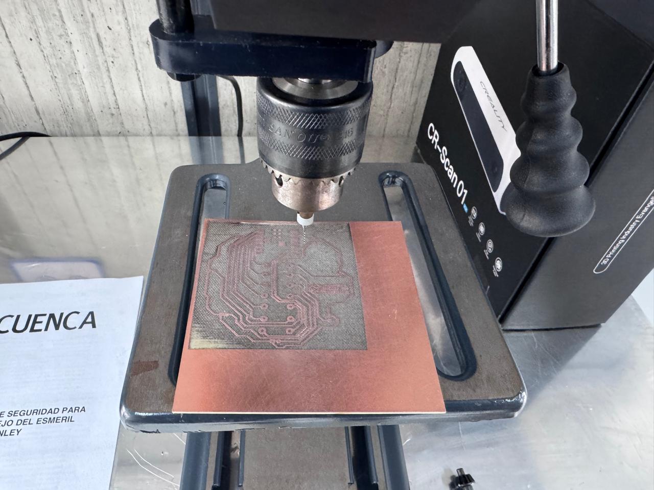
We used the provided drawings for the traces to generate a controlled fabrication test. The objective was to evaluate resolution, precision, and repeatability in both CNC milling and fiber laser processes under real manufacturing conditions.
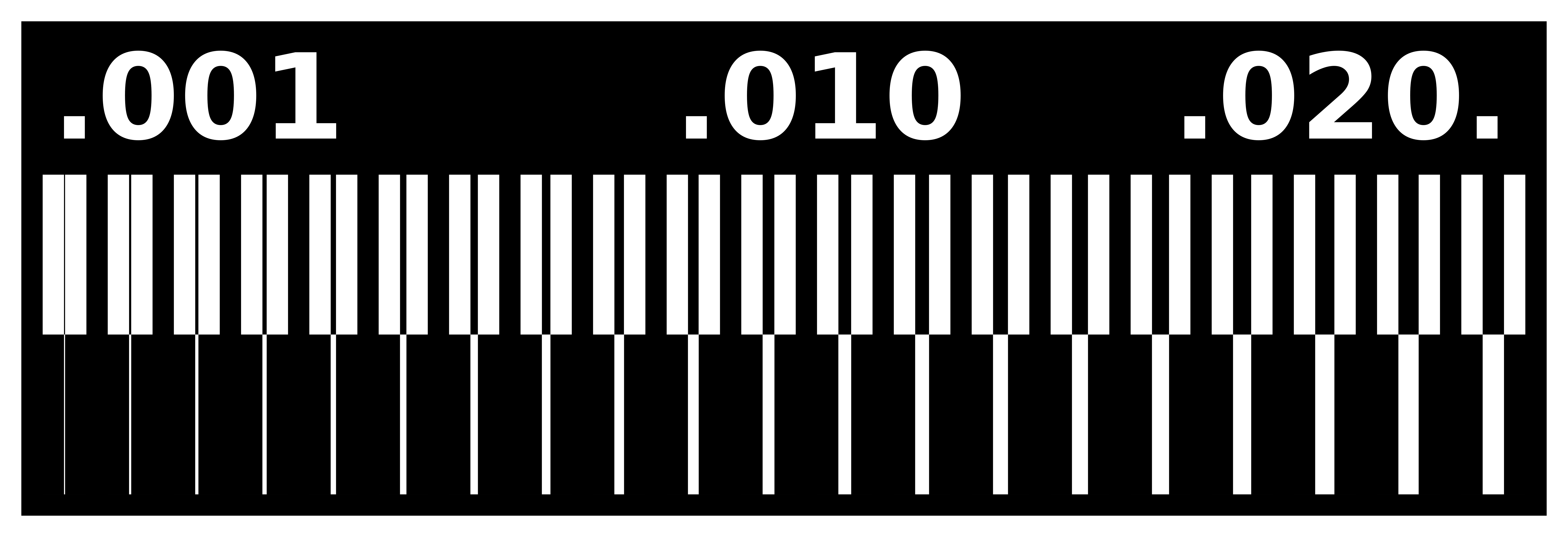
This comparative test highlights the differences between subtractive CNC milling and non-contact fiber laser machining, focusing on precision, repeatability, and fabrication efficiency.
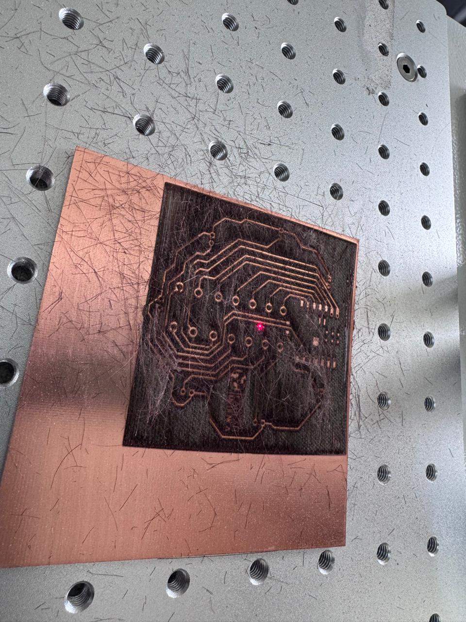
The fiber laser machine operates by emitting high-frequency pulses of energy that remove copper from the PCB surface through thermal ablation. This process is entirely contactless and controlled digitally.
Unlike milling, there is no mechanical force applied to the board. However, the process introduces thermal energy that can affect both the copper layer and the substrate.
Critical parameters:
Understanding the interaction between these variables is essential for achieving reliable PCB results.
A test PCB was designed to explore the limits of the fabrication process. This board included a range of geometries to evaluate resolution, spacing, and engraving quality.
The experimentation followed a structured iterative process:
This process was repeated multiple times to ensure consistent results and identify optimal fabrication conditions.
This section summarizes the results obtained from the PCB trace fabrication tests using two different manufacturing technologies: CNC milling and JPT 90W fiber laser. The comparison highlights performance differences, advantages, and limitations observed during the process.
.jpeg)
.jpeg)
Overall, CNC milling is more practical for fast prototyping and educational environments, while fiber laser machining provides superior precision and repeatability for advanced PCB fabrication.
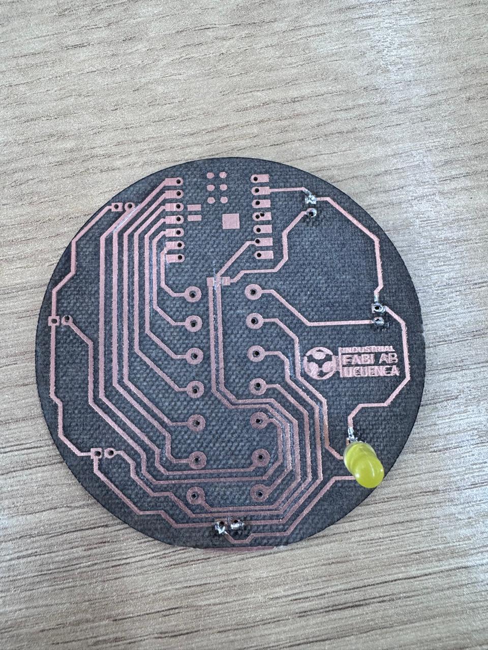
The individual assignment focused on applying the characterized process to fabricate a functional PCB capable of producing a LED roulette animation using a XIAO ESP32C3.
| Component | Quantity | Description |
|---|---|---|
| XIAO ESP32C3 | 1 | Main microcontroller |
| LEDs | 7 | Visual output |
| Resistors 220Ω | 7 | Current limiting |
| Copper PCB | 1 | Base material |
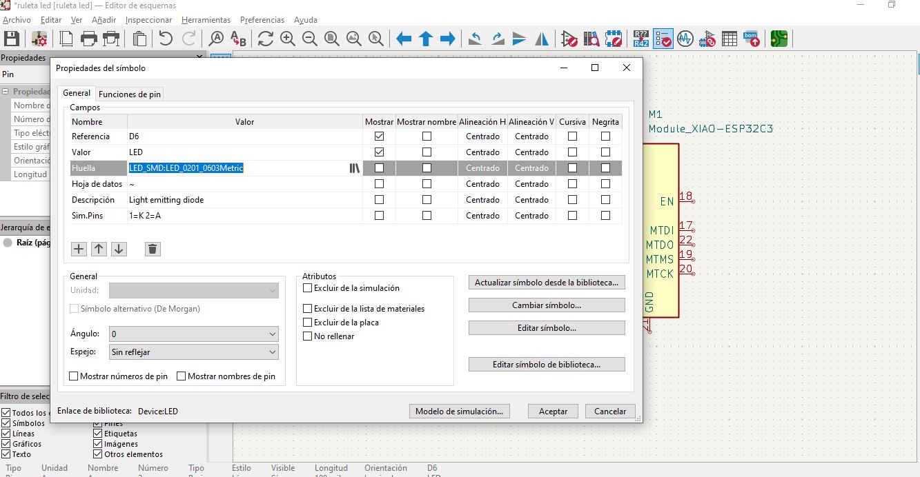
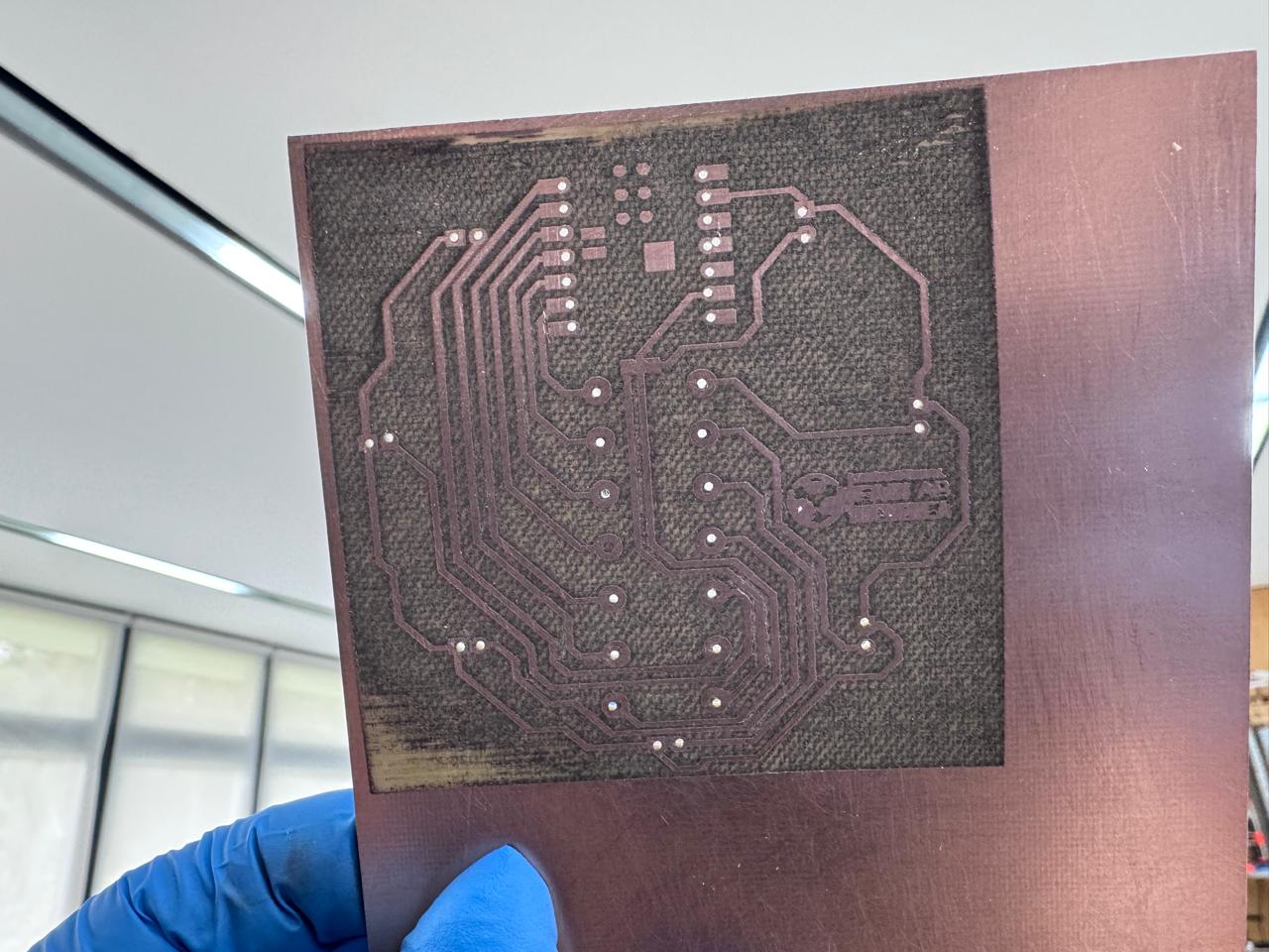
The design process began with the creation of a schematic in KiCad. This stage defines the logical structure of the circuit.
Each LED was connected to a dedicated GPIO pin from the XIAO ESP32C3 through a 220Ω resistor. This ensures proper current limiting and protects both the LED and the microcontroller.
Special attention was given to:
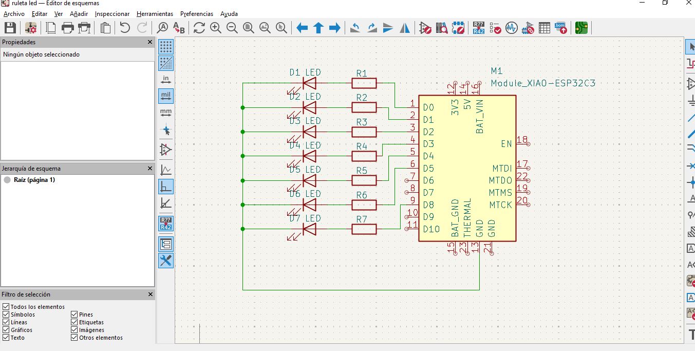
Electrical Rule Check (ERC) was executed to detect connection errors before proceeding.
After validating the schematic, the design was transferred to the PCB editor.
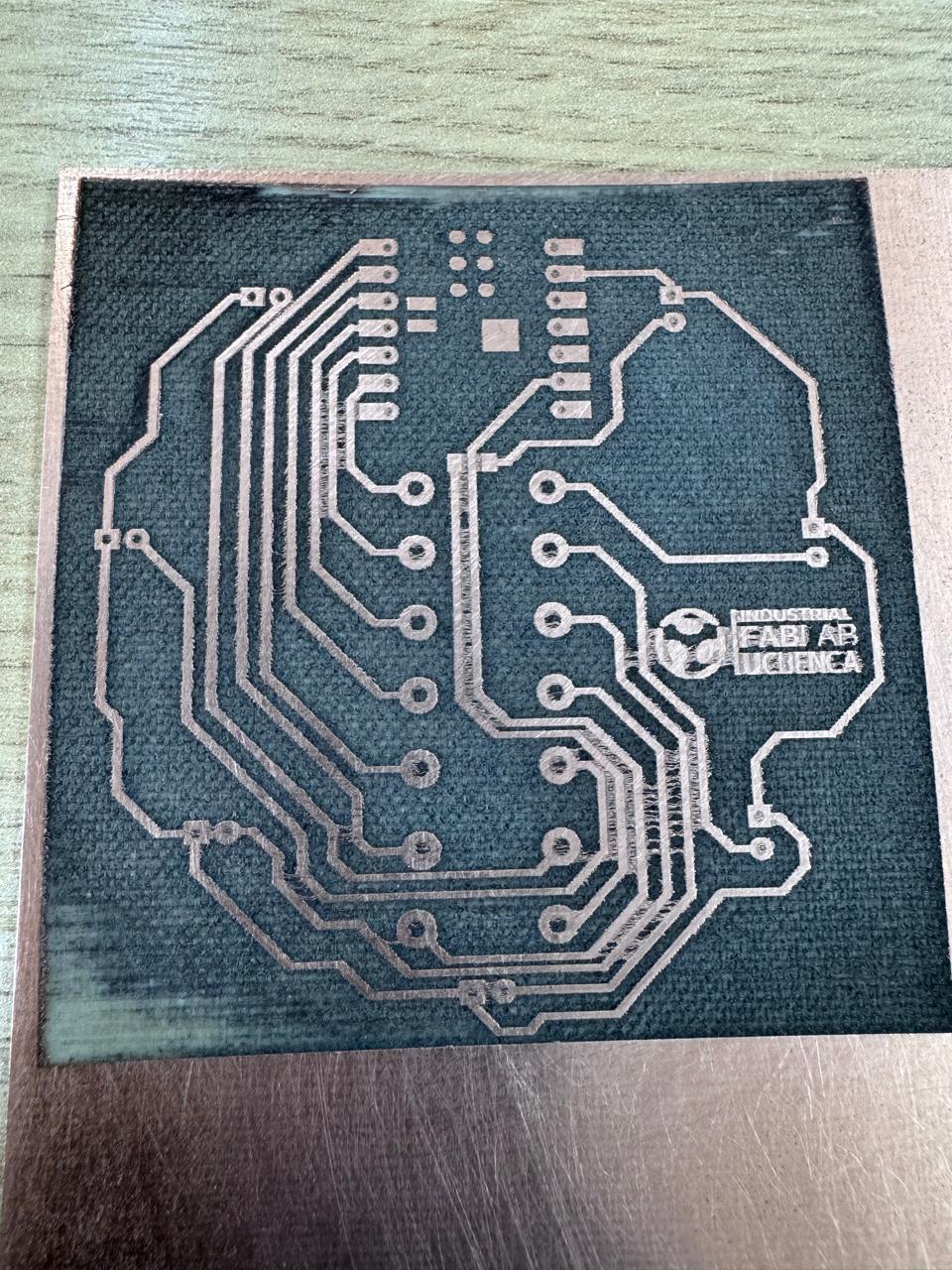
Components were placed with a clear intention: LEDs arranged in a circular geometry to visually simulate a roulette effect.
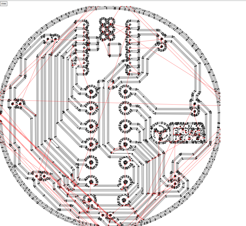
Routing required careful planning:
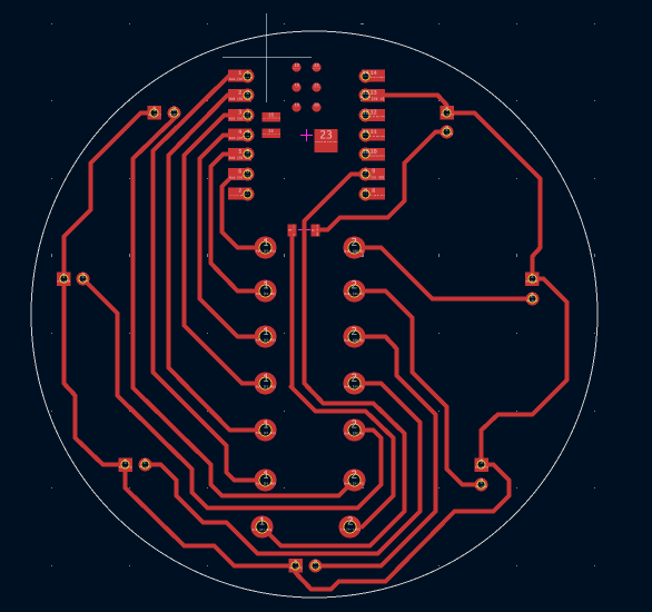
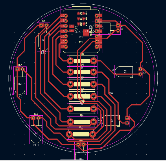
The design rules obtained in the group assignment were strictly followed to ensure manufacturability.
The PCB layout was exported and processed in Inkscape to generate a file compatible with the fiber laser.
This step is critical because the laser interprets graphical information directly.
Detailed process:
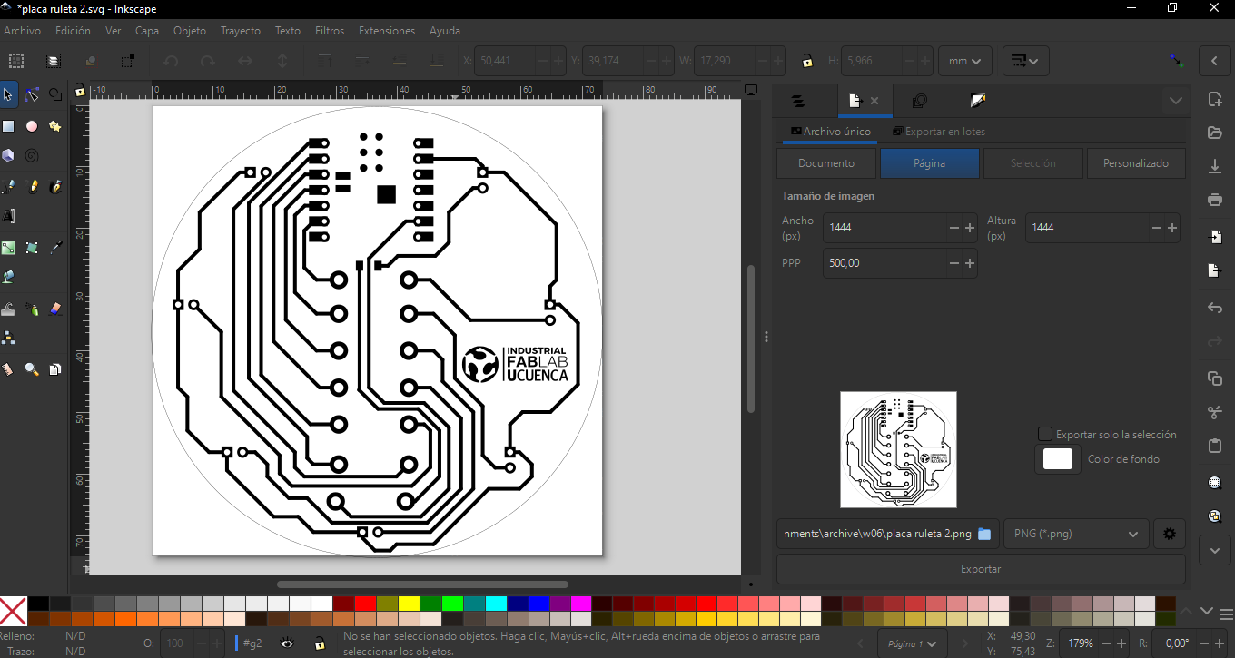
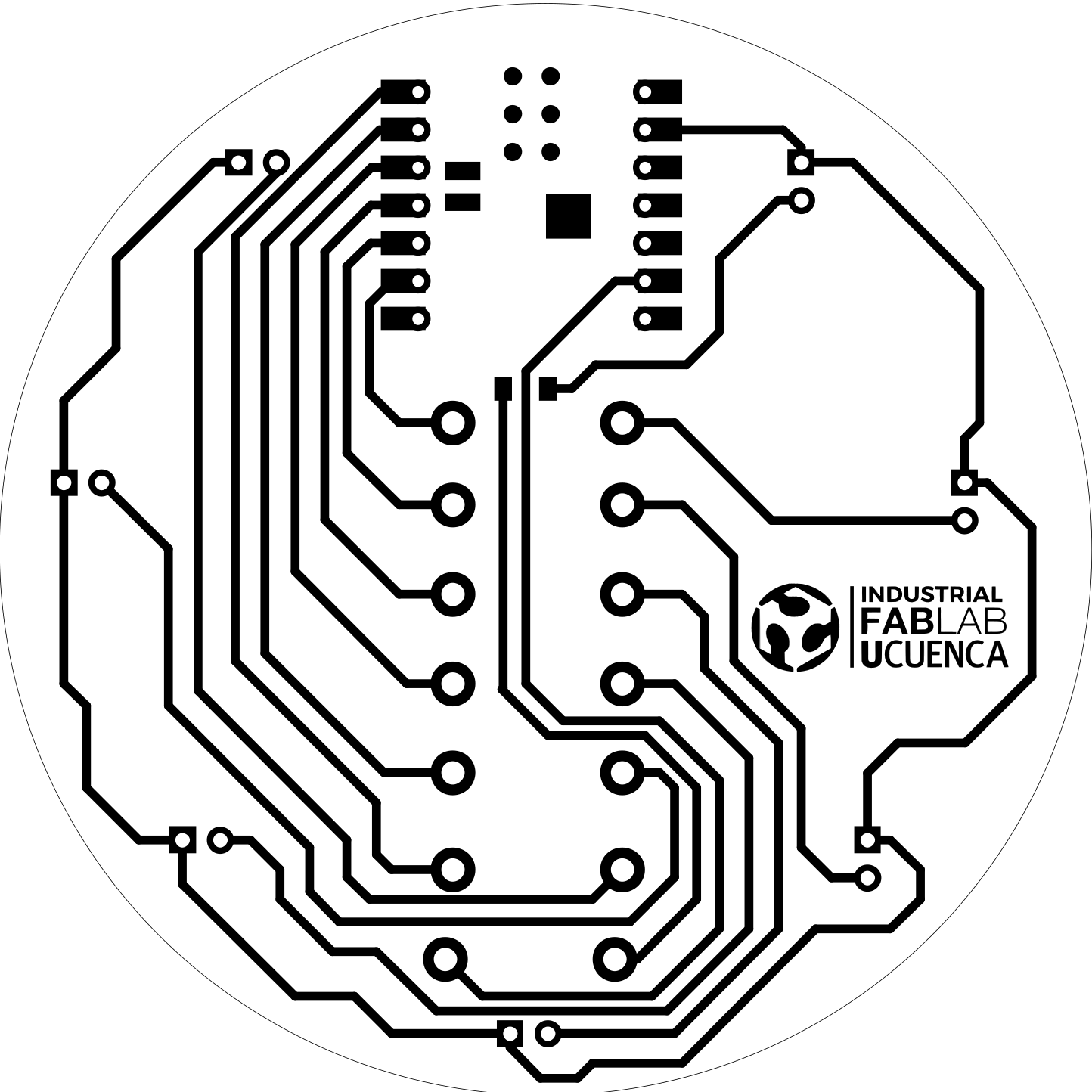
Any graphical error at this stage results in fabrication defects.
For this project, Fab Modules (Mods) were used to process the PCB design images and generate the corresponding G-code required for digital fabrication. This step is critical because it translates visual design data into machine instructions.
The workflow in Mods follows a modular structure where each node processes specific information. The objective was to convert a monochrome PCB image into precise toolpaths that define how the machine removes copper.
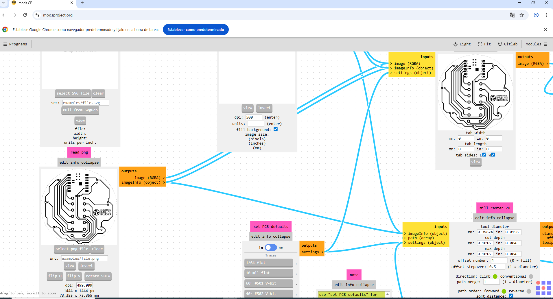
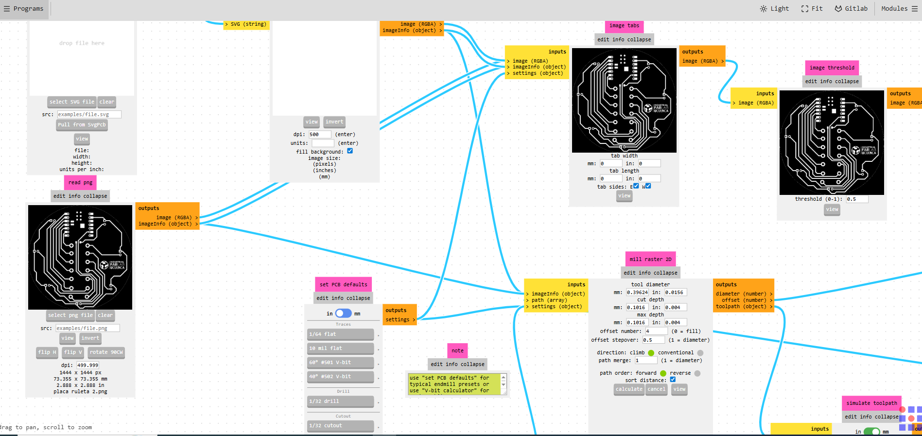
This step ensures that the digital design is accurately translated into machine movements, enabling precise PCB fabrication.
The engraving process defines the electrical circuit by removing copper.
Detailed workflow:
Parameter selection is critical:
Multiple passes were used to improve precision without overheating.
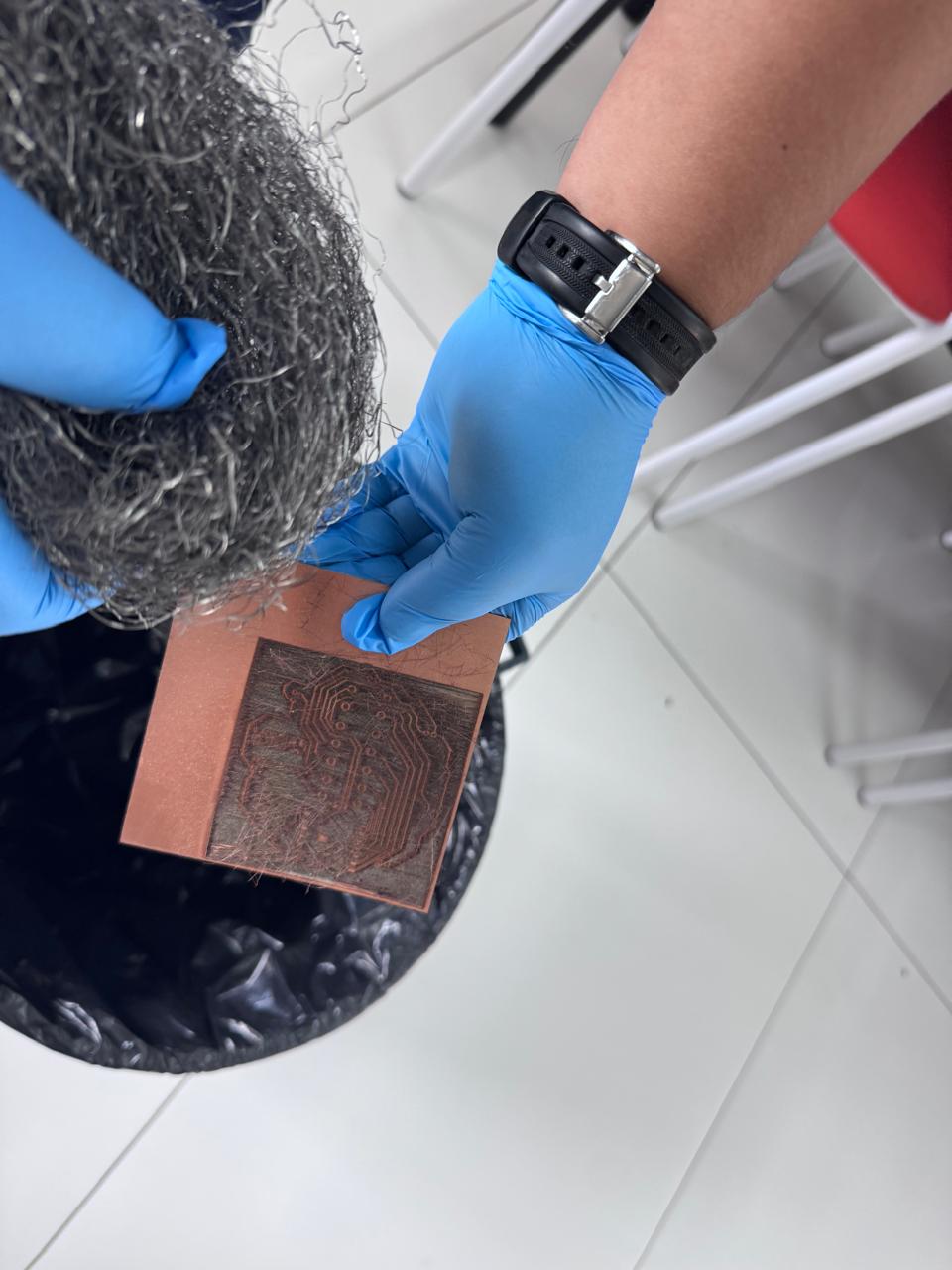
Once engraving was completed, holes were drilled for through-hole components.
Detailed process:
Improper drilling can lift copper pads or misalign components.
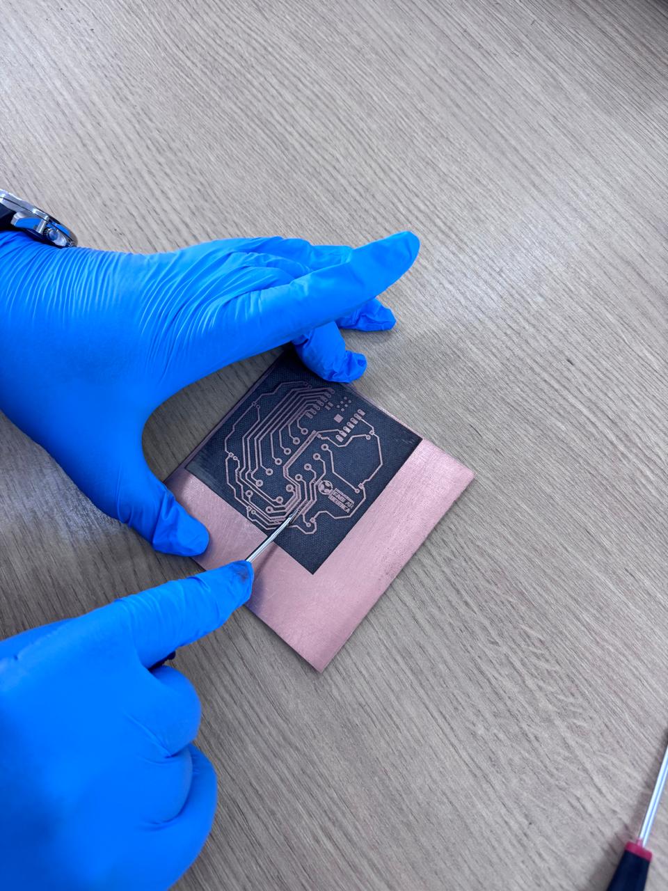
The final board shape was defined using a laser cutter.
Steps:
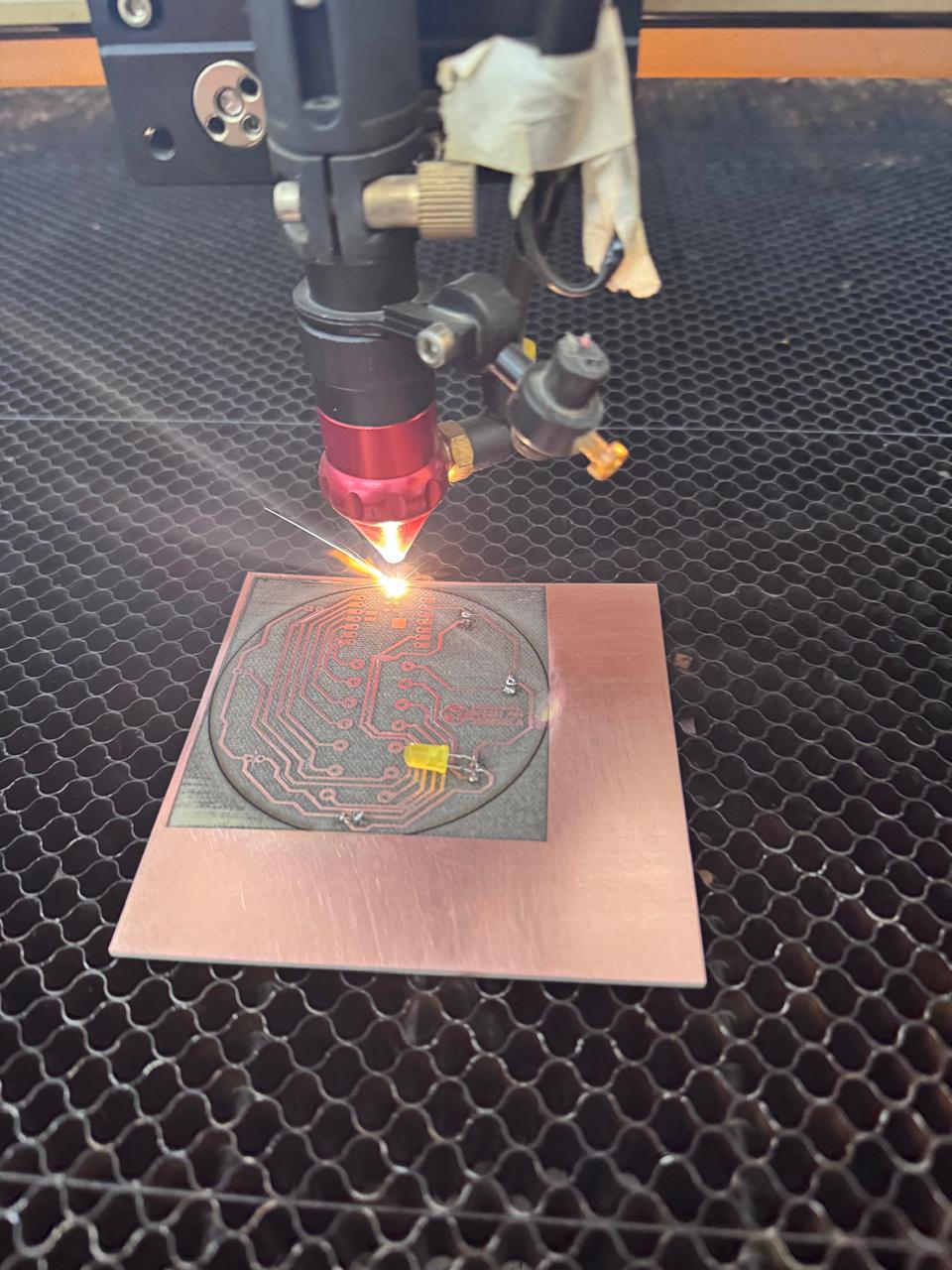
Cutting must be carefully aligned to preserve all traces and components.
All components were assembled using manual soldering.
Detailed process:
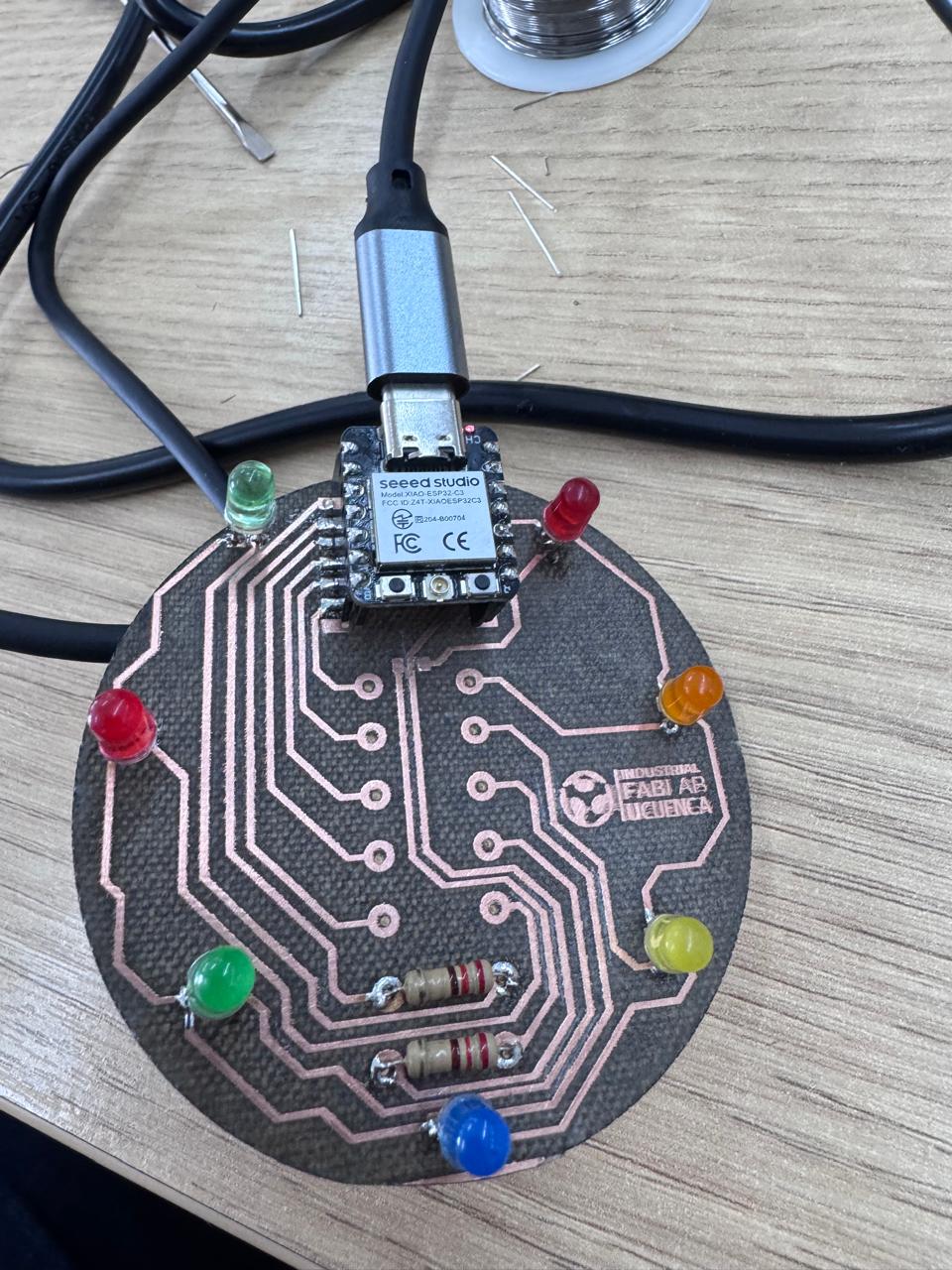
Polarity verification was essential for LEDs.
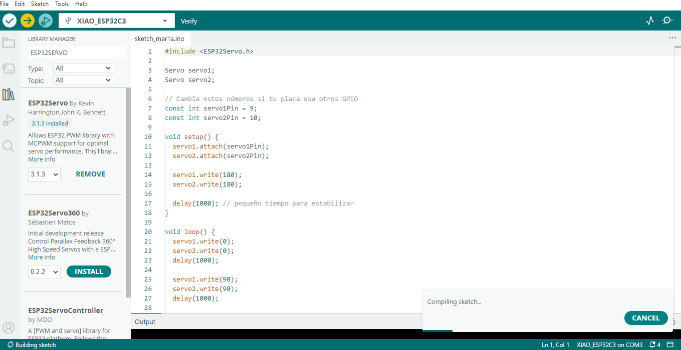
The XIAO ESP32C3 was programmed using Arduino IDE.
The code implemented a sequential activation of LEDs, simulating a rotating effect with progressive acceleration and final blinking.
 Download Arduino Code (.ino)
The system was tested to verify functionality.
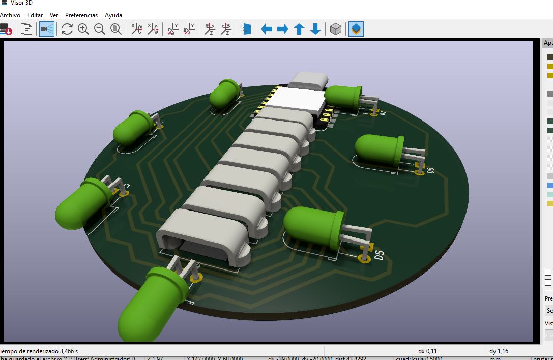
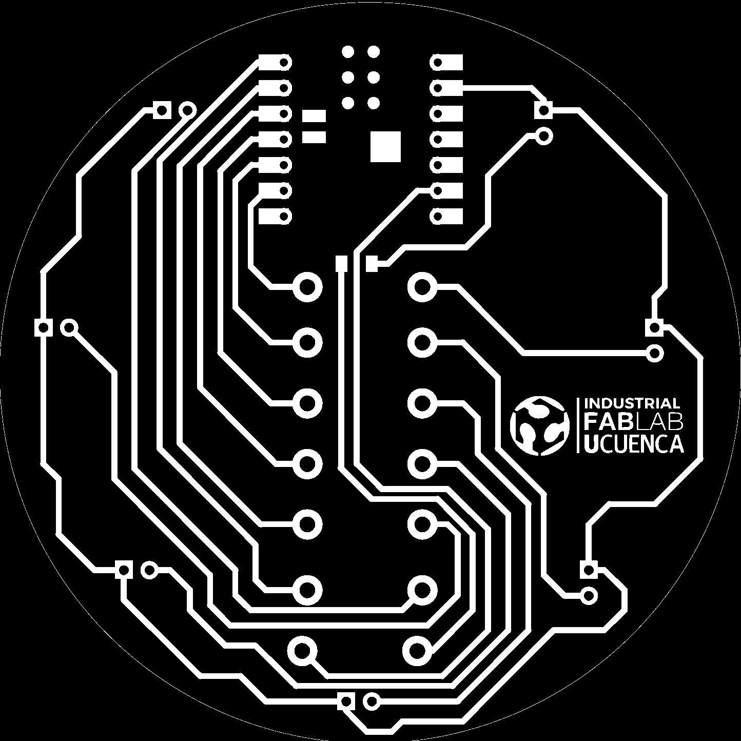
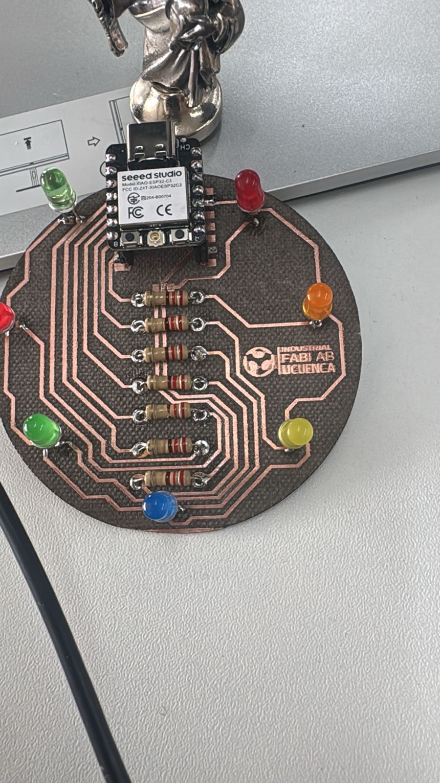
The final documentation included a high-quality image of the working PCB.
This image highlights the final result and demonstrates successful integration of design, fabrication, and programming.
This project demonstrated that PCB fabrication is not only a design challenge but also a manufacturing challenge.
The fiber laser method offers flexibility and speed, but requires precise calibration and understanding of thermal effects.
The integration of all stages resulted in a functional and well-documented embedded system.
This assignment demonstrated the complete workflow of PCB fabrication, integrating design, manufacturing, and programming into a single process. The use of a fiber laser introduced a non-traditional method that required careful parameter calibration and a deep understanding of thermal effects on materials.
Through iterative testing, it was possible to establish reliable design rules and validate the feasibility of this fabrication method. The integration of tools such as KiCad, Inkscape, and Fab Modules (Mods) ensured a consistent transition from digital design to physical implementation.
The final result, a fully functional LED roulette controlled by the XIAO ESP32C3, confirms that the workflow was successful. This process reinforced the importance of precision, testing, and multidisciplinary integration in digital fabrication.