NODO

Electronic design
The objective of this group assignment is to use the available test equipment in the lab to observe and analyze the operation of a microcontroller-based circuit board. This involves understanding how signals behave in real time and how different components interact within the system.
As a minimum requirement, the use of a logic analyzer must be demonstrated. This tool allows capturing and visualizing digital signals, making it possible to inspect communication protocols, timing relationships, and signal integrity between components.
Through this activity, the goal is to gain practical experience in debugging and validating embedded systems using professional measurement tools, reinforcing theoretical knowledge with real-world observation.
All findings, procedures, and results must be documented on the group assignment page. Additionally, each team member should include a personal reflection on their individual page, describing what they learned and how the experience contributed to their understanding of microcontroller systems and electronic testing.
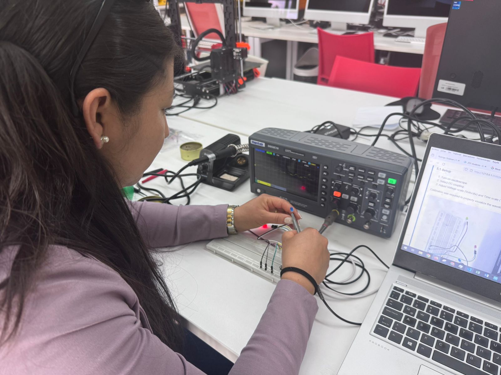
Open Group AssignmentThis week’s group assignment consisted of learning how to use laboratory test equipment to observe and analyze the operation of a microcontroller circuit board.
As a minimum requirement, we demonstrated the use of:
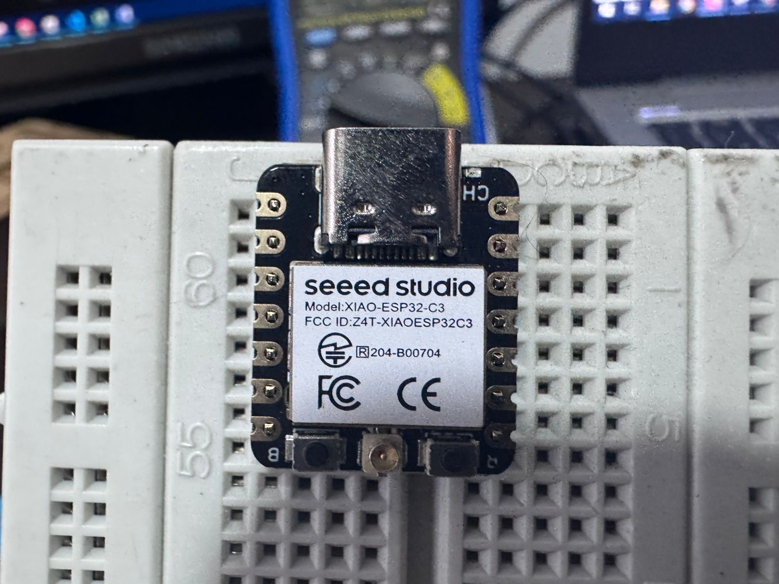
The system under test was an ESP32-C3 development board powered via USB (5V) and operating at 3.3V logic level.
The objective was to understand how electrical signals behave in real hardware and to validate circuit functionality before moving into PCB design.
| Equipment | Description | Useful For |
|---|---|---|
| Regulated Power Supply | Provides stable DC voltage independent of input fluctuations. | Safely powering circuits during testing. |
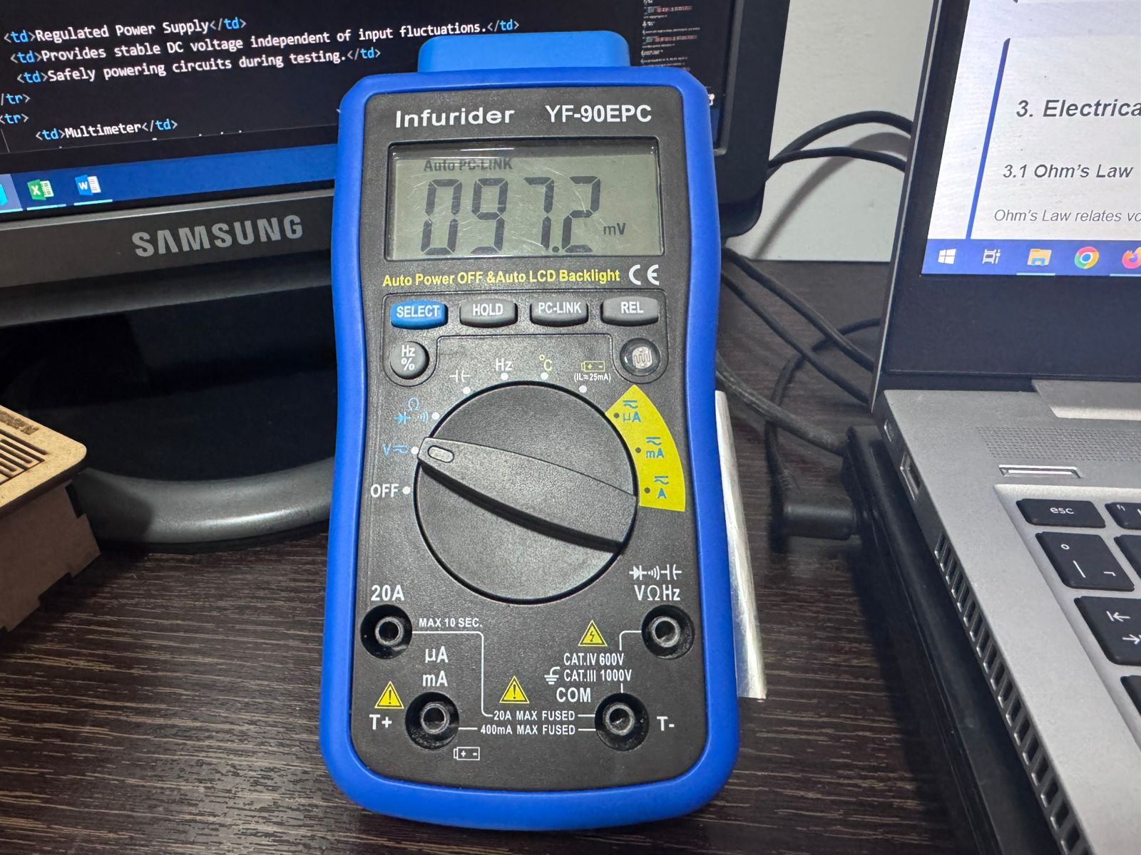
| Multimeter | Measures Voltage (AC/DC), Current, Resistance, Continuity, and sometimes Capacitance. | Diagnosing circuit issues and verifying correct electrical values. |
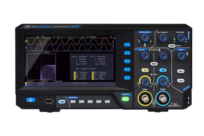
| Oscilloscope | Displays voltage as a function of time (Voltage vs Time). | Observing waveform shape, frequency, amplitude, and signal integrity. |
| Logic Analyzer | Captures multiple digital signals simultaneously. | Analyzing digital communication and logic states. |
| Mixed Signal Oscilloscope | Combines analog and digital signal analysis. | Testing circuits with both analog and digital components. |
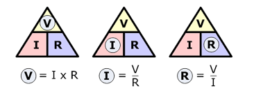
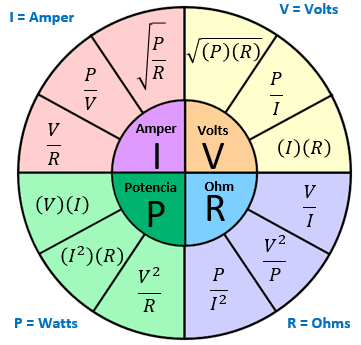
Ohm’s Law relates voltage, current, and resistance:
V = I × R
Where:
V = Voltage (Volts)
I = Current (Amperes)
R = Resistance (Ohms)
Derived forms:
I = V / R
R = V / I

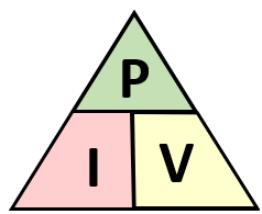
Power is the rate at which electrical energy is consumed.
P = V × I
Alternative forms using Ohm’s Law:
P = I² × R
P = V² / R
Where:
P = Power (Watts)
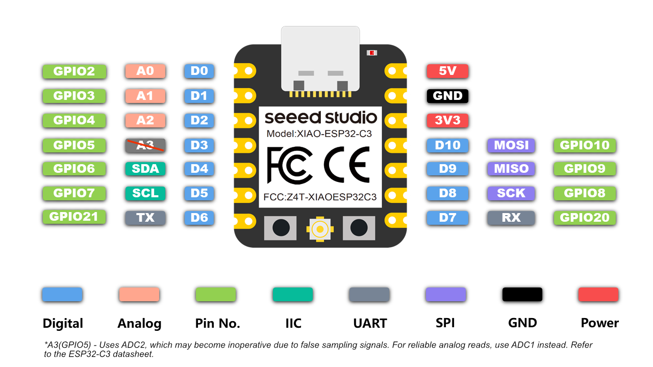
ESP32-C3 GPIO = 3.3V
LED forward voltage ≈ 2.0V
Desired current = 5mA (0.005A)
R = (3.3V − 2.0V) / 0.005A
R = 260Ω
Standard value used: 220Ω
Power dissipation in resistor:
P = V × I
P = 1.3V × 0.005A
P = 0.0065W (6.5mW)
A 1/4W resistor is more than sufficient.
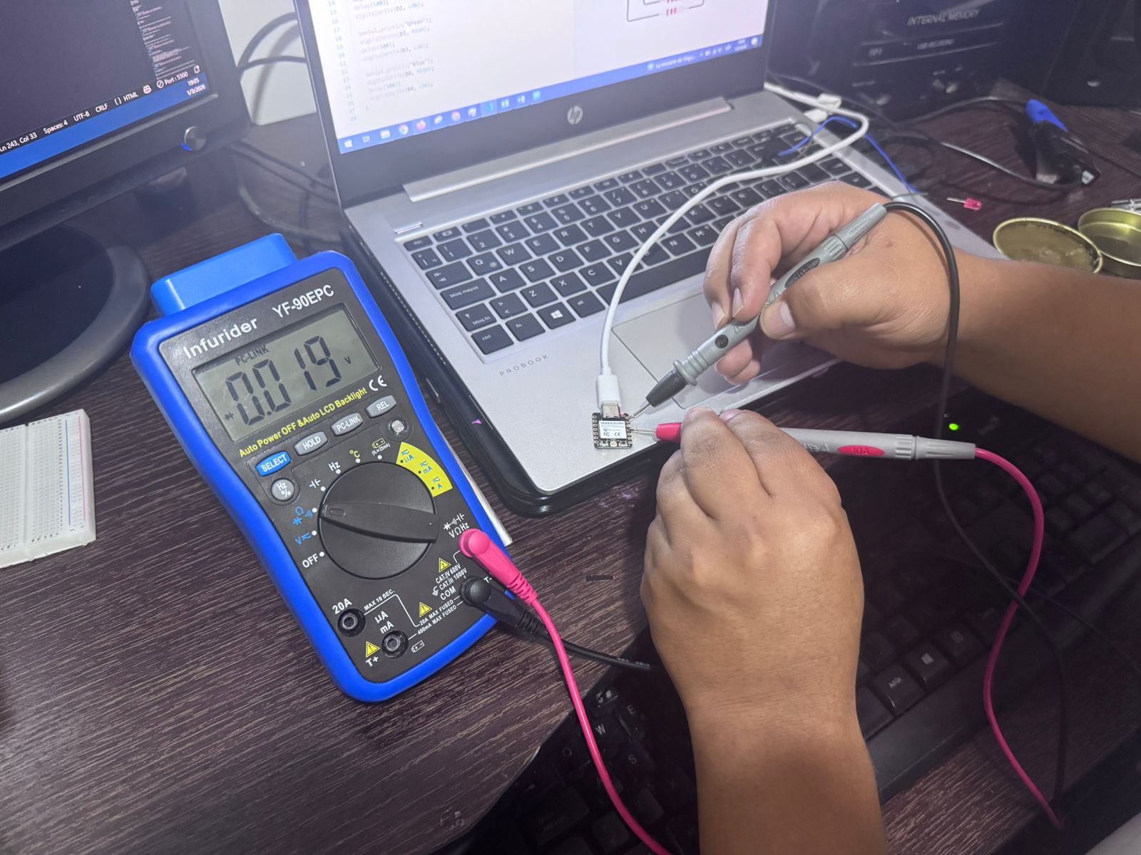
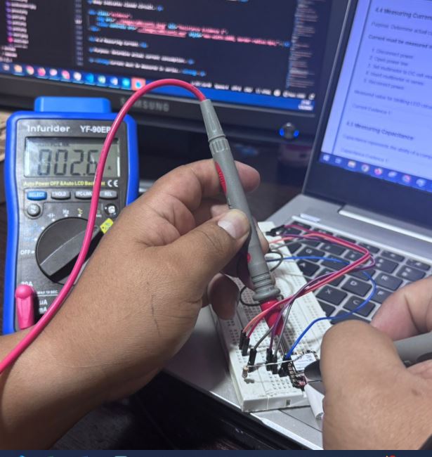
Purpose: Verify correct power supply levels.
Measurements performed:
Working battery → 8.9V
Dead battery → 1.2V
ESP32-C3 3.3V output → 3.2V
This confirmed proper voltage regulation.
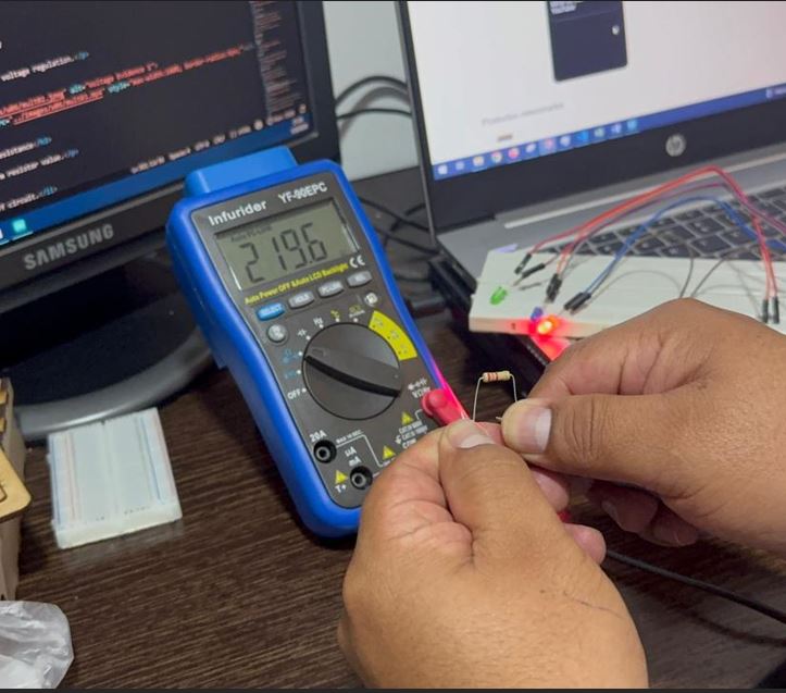
Purpose: Confirm resistor value.
Measured value: 220Ω
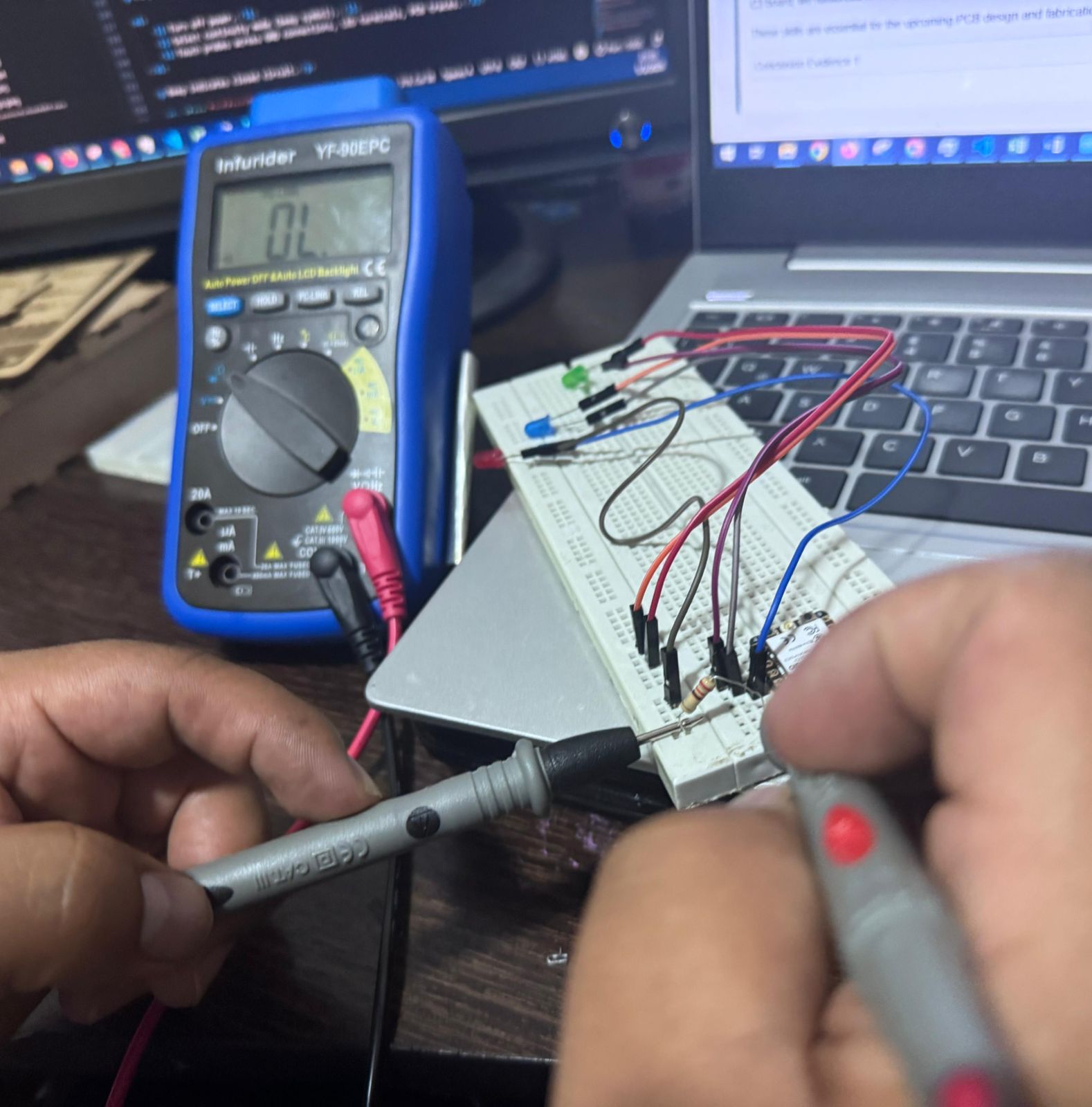
Purpose: Ensure circuit connections are closed and solder joints are correct.
Beep indicates closed circuit.
Purpose: Determine actual current consumption.
Current must be measured in series.
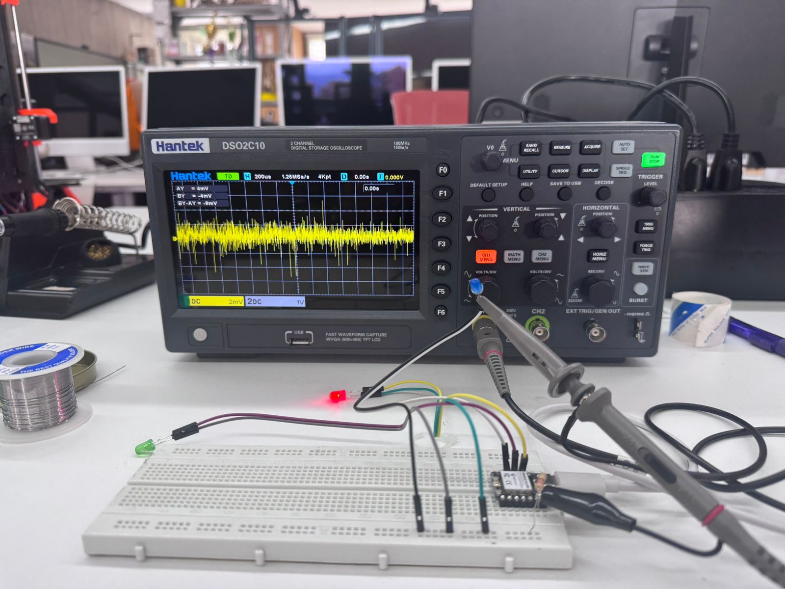
Measured value for blinking LED circuit: 5.4 mA
Calibration was required to properly visualize the waveform.
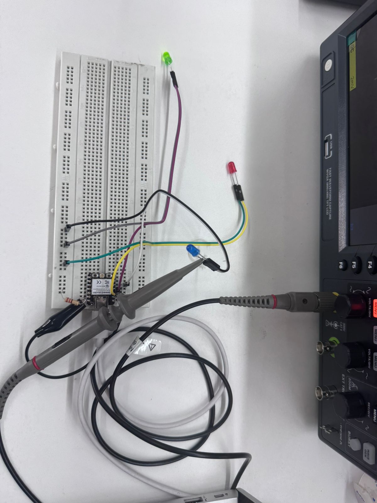
The ESP32-C3 was programmed with a blinking LED (100 ms interval).
Probe connections:
Tip → GPIO pin
Ground clip → GND
Observed waveform:
Square wave
0V (LOW)
3.3V (HIGH)
LOW = 500 ms
HIGH = 100 ms
The waveform width changed accordingly, demonstrating duty cycle variation.
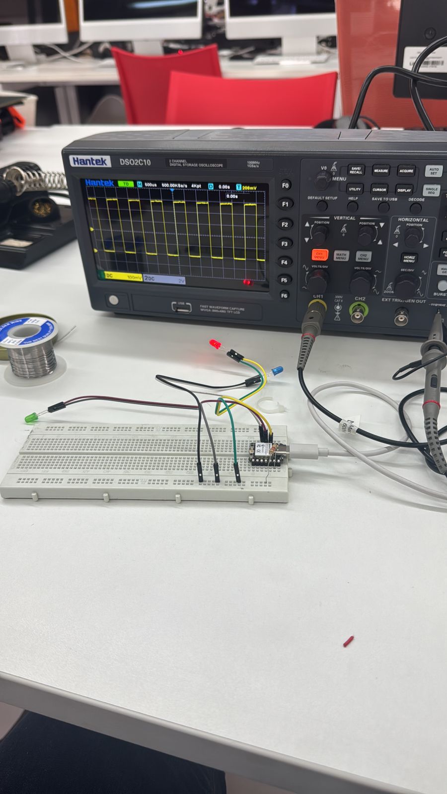
We transmitted character “K”. ASCII binary: 111101011
Oscilloscope displayed Start bit (0), Data bits, Stop bit (1).
This confirmed correct digital serial transmission.
This group assignment provided practical experience using laboratory test equipment to analyze a microcontroller system. By validating electrical parameters on the ESP32-C3 board, we reinforced fundamental concepts such as Ohm’s Law, power dissipation, signal integrity, and digital waveform behavior.
These skills are essential for the upcoming PCB design and fabrication stages, where electrical validation becomes critical before hardware deployment.
For this assignment, I designed a custom electronic system using KiCad as the Electronic Design Automation (EDA) software. The project integrates a Seeed Studio XIAO ESP32-C3 microcontroller to control two servo motors.
The workflow included:
KiCad is an open-source Electronic Design Automation (EDA) tool used to design schematics and printed circuit boards (PCBs).
It allows:
KiCad is widely used in academic and professional electronics development due to its flexibility and open-source ecosystem.
The system consists of:
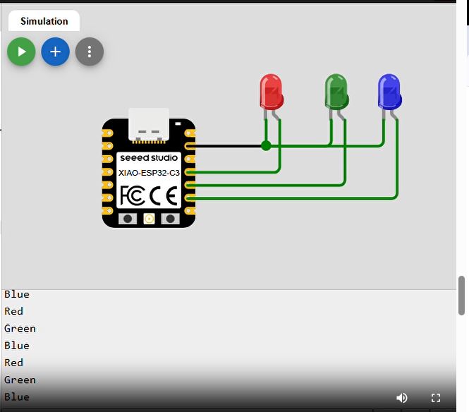
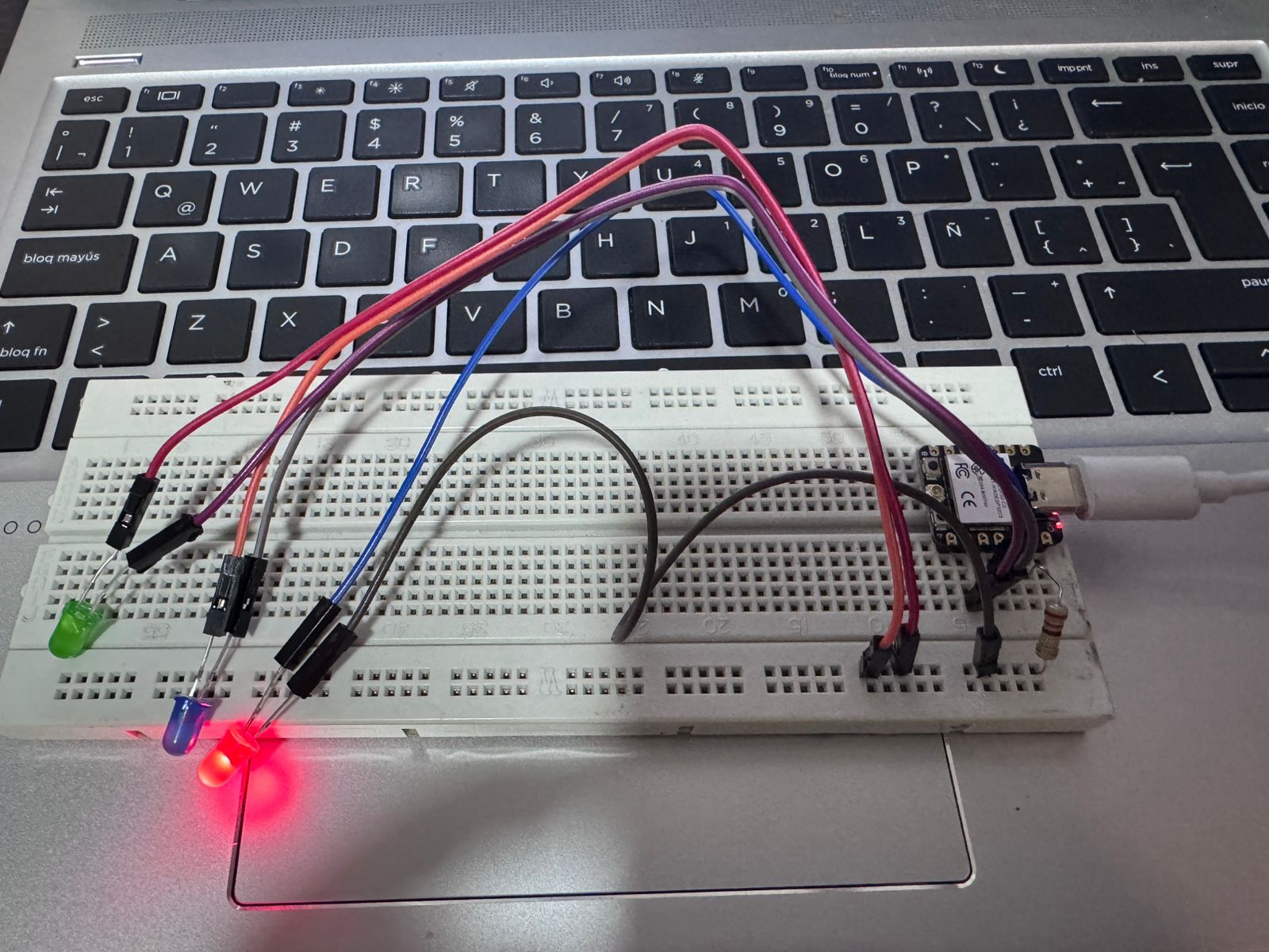
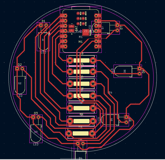
This circuit is designed to simulate a roulette effect using 7 LEDs controlled by a Seeed XIAO ESP32-C3 microcontroller. The system sequentially activates each LED to create a dynamic visual pattern, similar to a spinning wheel that eventually stops at a random position.
Each LED is connected to a dedicated GPIO pin of the XIAO ESP32-C3:
Each LED is connected in series with a resistor to protect it from excessive current:
This configuration ensures that when a GPIO pin outputs HIGH (3.3V), the corresponding LED turns ON, and when LOW, it turns OFF.
The program controls the LEDs in a sequential loop:
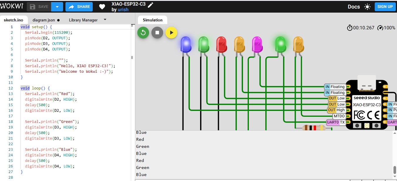
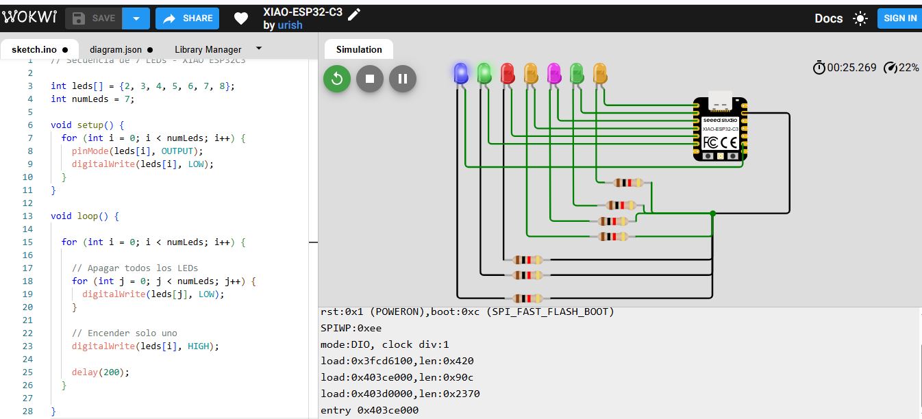
The LED roulette system was first validated using Wokwi, an online simulation platform that allows testing both circuit connections and embedded code before implementing the design in physical hardware.
Using Wokwi significantly improves the development workflow by ensuring that both the circuit design and the program logic are correct before assembling the real system.
Before designing the PCB, the system was simulated using Wokwi.
Steps:
After validating the simulation, the firmware was developed in Arduino IDE.
Steps:
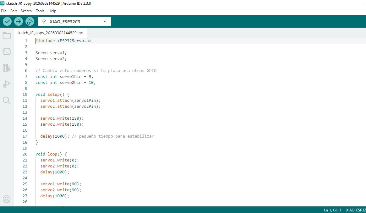
The program controls two servos using PWM signals and predefined movement sequences.
To follow Fab Academy PCB standards, the Fab library was installed.
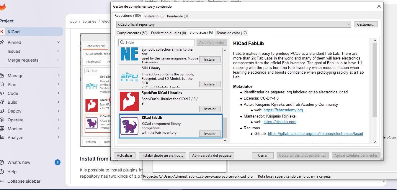
This enables access to Fab-standard components such as resistors, capacitors, pin headers and microcontrollers.
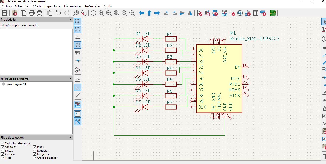
The schematic of the LED roulette system was developed using KiCad, an open-source electronic design automation (EDA) tool. This stage is essential to define electrical connections clearly before moving to PCB design or physical prototyping.
This schematic design process ensures a clear and reliable representation of the circuit, serving as the foundation for both simulation, PCB fabrication, and physical implementation.
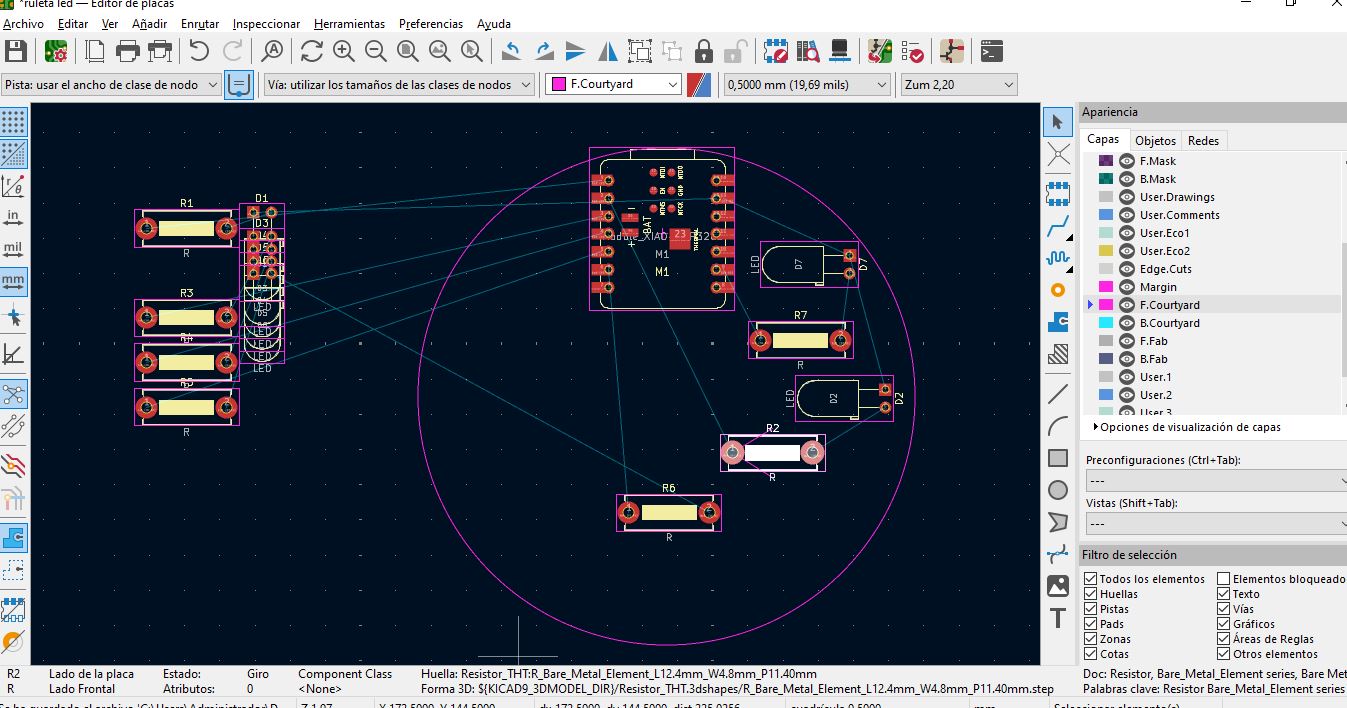
Open Tools → Assign Footprints.
Save and update PCB.
Open PCB Editor.
Step 1: Define Board Outline
Use Edge.Cuts layer to draw rectangular board shape.
Step 2: Place Components
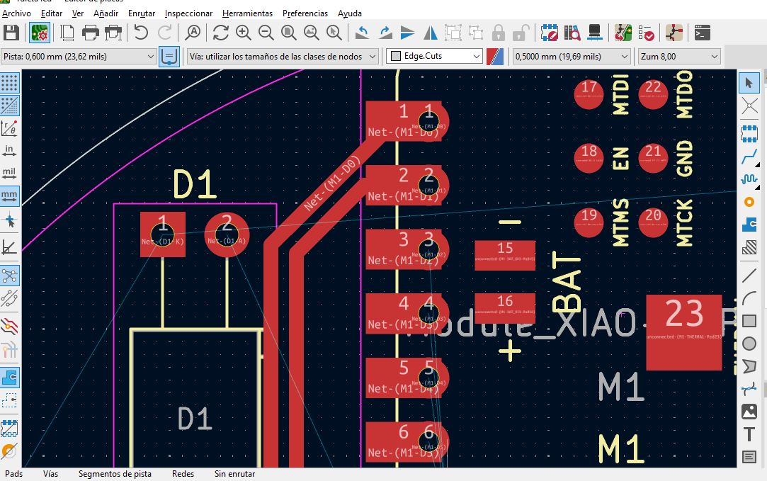
Before routing the PCB, I defined design rules in KiCad to make sure the board could be fabricated and soldered reliably. These rules establish the minimum distances and sizes allowed in the layout. However, the values are not universal: they depend on the fabrication method. In the lab, two possible PCB fabrication situations must be considered: a CNC router for PCB milling and a fiber laser machine for copper engraving.
The rules were selected according to four criteria: the machine used to fabricate the PCB, the minimum feature size that the process can reproduce, the current carried by each trace, and the complexity of routing around the XIAO ESP32-C3 and output components. Signal traces for GPIO lines can be thinner, while power and ground traces need more width because they carry more current and provide a stable reference for the circuit.
When the board is fabricated with a CNC router, the design must respect the physical diameter of the milling tool. The isolation between copper areas depends on the tool path, so the clearance must be large enough for the cutter to remove copper without leaving bridges. For this reason, CNC-routed PCBs usually need more conservative clearances and trace widths.
| Rule | CNC Router Value | Criteria |
|---|---|---|
| Minimum clearance | 0.40 mm | Allows the milling bit to isolate copper areas without leaving unwanted bridges. |
| Signal trace width | 0.40 mm | Keeps GPIO traces strong enough after mechanical milling. |
| Power trace width | 0.60 mm - 0.80 mm | Improves current capacity and reduces the risk of thin traces breaking. |
| Copper zone clearance | 0.50 mm | Prevents the GND fill from becoming too close to signal traces after milling. |
| Track angle | 45 degrees preferred | Improves inspection and avoids fragile corners in mechanically milled traces. |
When the board is fabricated with a fiber laser, the process is different. The laser does not remove copper with a rotating tool, so it can produce finer details. However, the quality depends strongly on laser power, speed, focus, number of passes, and copper cleaning. The main risk is not tool diameter, but incomplete copper removal, burn marks, and small conductive bridges left between traces.
| Rule | Fiber Laser Value | Criteria |
|---|---|---|
| Minimum clearance | 0.25 mm - 0.30 mm | The laser can engrave finer isolation, but the result must be inspected with continuity tests. |
| Signal trace width | 0.30 mm - 0.40 mm | Fine GPIO traces are possible, but wider traces are safer for soldering and rework. |
| Power trace width | 0.50 mm - 0.70 mm | Power traces still need more copper area even if the fabrication process allows smaller geometry. |
| Laser offset margin | 0.10 mm test margin | Used to compensate for laser kerf, focus variation, and possible overburn around traces. |
| Inspection method | Visual inspection + continuity test | Every power, GND, and signal path must be checked because small copper bridges can remain after engraving. |
The following image documents the design rules panel used as reference for this PCB. It summarizes the difference between CNC router rules and fiber laser rules. The CNC rules are more conservative because the milling tool needs physical isolation space. The fiber laser rules can be finer, but they require careful calibration and electrical verification after engraving.

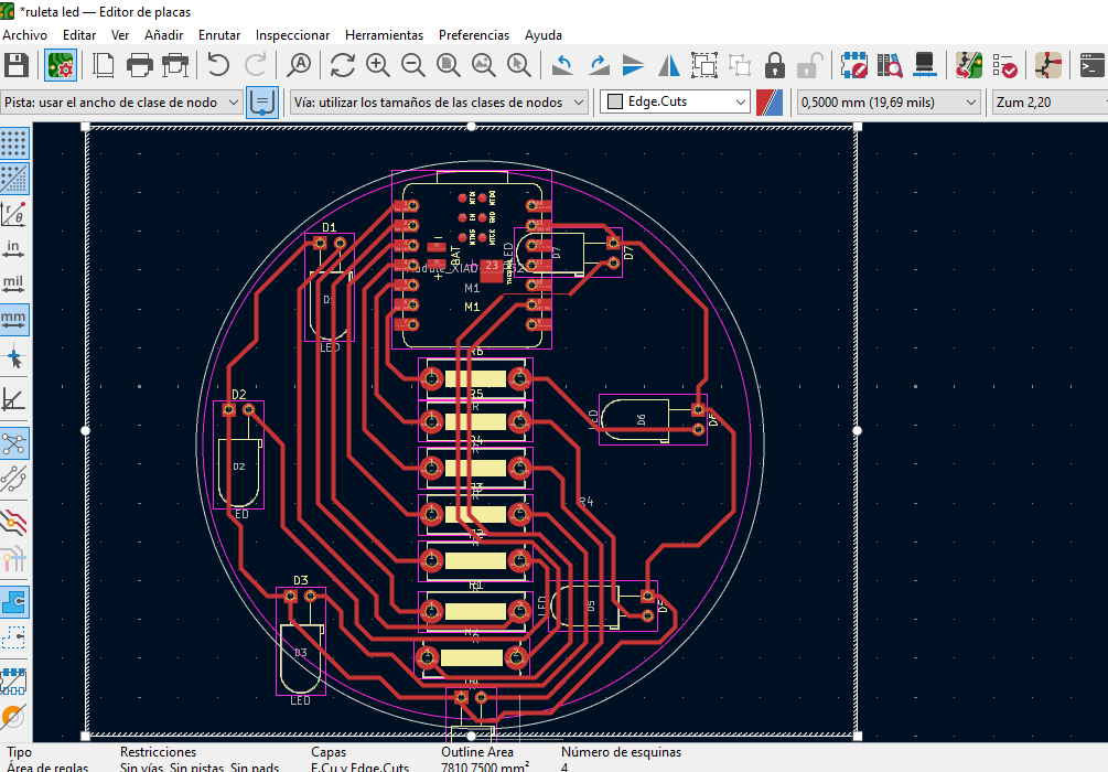
The Electrical Rules Check was used in the schematic before transferring the design to the PCB editor. This helped detect electrical problems early, especially missing references and pins that were not clearly connected.
During PCB routing, the most common issues were clearance violations, tracks too close to pads, and routes that crossed each other near the microcontroller headers. These problems were corrected iteratively by moving components, increasing track spacing, and rerouting signals with cleaner 45 degree paths.
| Problem | Cause | Correction |
|---|---|---|
| Clearance violation | Tracks were too close to neighboring pads near the connectors. | Increased spacing and rerouted the trace around the connector footprint. |
| Unconnected net | A route looked connected visually but did not actually reach the pad center. | Used DRC markers, reconnected the track, and confirmed the ratsnest disappeared. |
| Power trace too thin | Initial routing used the same width for power and signal traces. | Changed 5V and GND paths to wider traces and used a GND copper fill. |
| Difficult routing around XIAO headers | The microcontroller pins are close together and many signals leave from the same area. | Reordered connector positions and used shorter, cleaner signal paths. |
After each correction, I ran DRC again until the board no longer showed critical errors. This process demonstrated that PCB design is iterative: the first route is rarely final, and the rules help transform the design into a board that can actually be fabricated and tested.
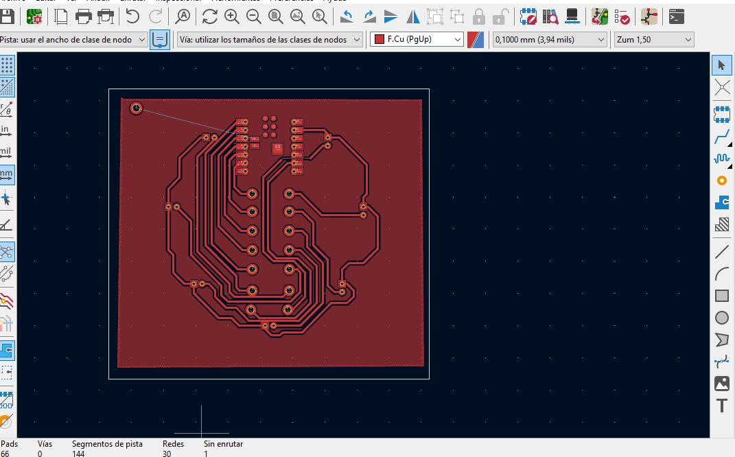
Benefits include reduced noise, better current return path and improved EMI performance.
Run DRC and inspect clearance violations, overlapping pads and unconnected nets.
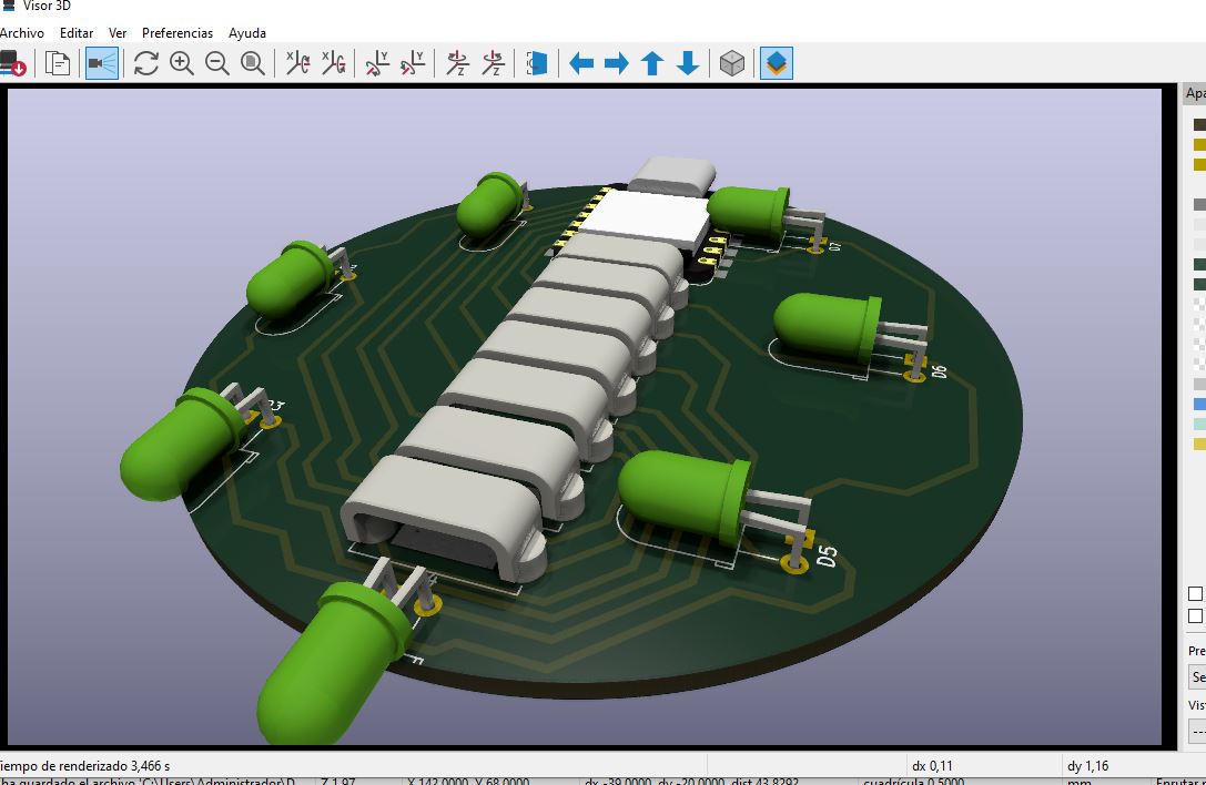
Open 3D Viewer and verify component placement, connector orientation and mechanical fit.
This assignment provided a comprehensive understanding of the complete workflow in electronics design, from schematic creation in KiCad to PCB fabrication and embedded programming using the XIAO ESP32-C3. It reinforced key concepts such as GPIO control, circuit design rules, and the relationship between hardware and software.
Additionally, the integration of simulation tools, PCB design, and real-world testing allowed a better understanding of how theoretical knowledge is applied in practical scenarios. The LED roulette system demonstrated how multiple outputs can be controlled efficiently to generate dynamic behaviors.
Overcoming these challenges strengthened problem-solving skills and highlighted the importance of iterative design, testing, and validation. The experience demonstrated that successful electronic system development requires careful planning, attention to detail, and continuous debugging.