Electronics Design — KiCad
Designing an electronic board in KiCad, documenting schematic creation, footprint selection, PCB layout, checks, and manufacturing-ready outputs.
Assignment
Electronics Design
Design Tool
KiCad
Output
Schematic + PCB
Status
In Progress
Goal: Design a functional board in KiCad and prepare it for fabrication.
🧠 Learning Objectives
- Design a complete electronic circuit schematic in KiCad.
- Assign correct footprints and create a manufacturable PCB layout.
- Run validation checks and prepare final fabrication files.
📌 Documentation Requirements (Checklist)
-
Show the full process
From idea and schematic to PCB layout and export files.
-
Document design decisions
Explain why each component and connection was used.
-
Show evidence
Include screenshots of schematic, PCB layout, and checks.
-
Provide manufacturing files
Attach KiCad project, exports, and fabrication-ready outputs if possible.
🛠️ Tools & Components
- EDA Software: KiCad
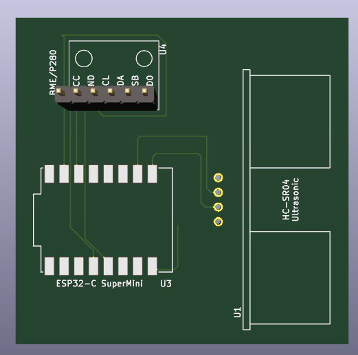
- Microcontroller: ESP32
- Components: Ultrasonic sensor (HC-SR04), Tempreature sensor (BMP280), Sparkfun OLE Display
- Manufacturing Process: PCB milling / PCB fabrication (replace based on your workflow)
Why KiCad? It allows schematic design, footprint assignment, PCB routing, checks, and file export in one workflow.
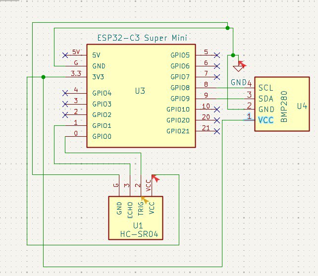
📐 Schematic Design
I started by defining the circuit’s purpose and selecting the required components. Then I created the schematic in KiCad, connecting each component according to its function.
- Power section: voltage input, VCC, and GND connections
- Microcontroller section: main control logic and pin mapping
- Input/Output section: sensors
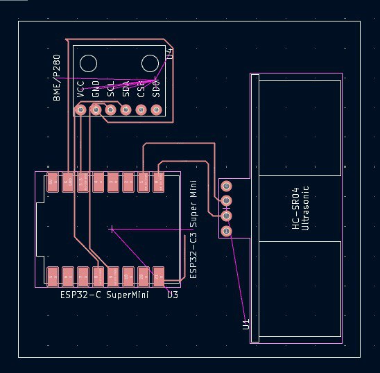
📦 Footprint Assignment
After completing the schematic, I assigned footprints to each component to match the parts I plan to use during fabrication and assembly.
- Selected footprints that match the package type of each component.
- Verified pad spacing and sizes for manufacturability.
- Checked orientation and pin numbering before moving to the PCB editor.
Important: Incorrect footprint selection can make the PCB impossible to assemble, even if the schematic is correct.
🧭 PCB Layout
In the PCB editor, I arranged the components to make routing easier and to keep the board compact and organized.
- Placed the microcontroller first as the main reference point.
- Positioned connectors and headers based on accessibility.
- Kept power traces clear and organized.
- Routed signal traces while minimizing crossing and unnecessary turns.
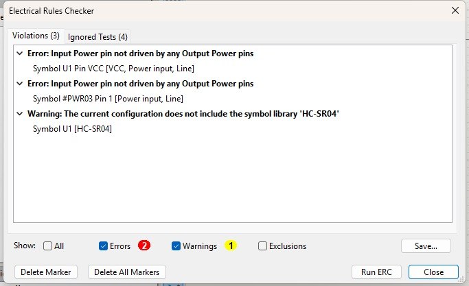
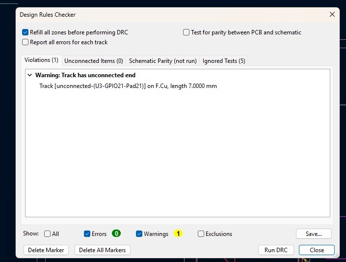
✅ ERC / DRC Validation
Before exporting the final files, I ran KiCad’s validation checks:
- ERC (Electrical Rules Check): confirmed that the schematic connections were valid.
- DRC (Design Rules Check): checked spacing, trace widths, and layout issues in the PCB.
Any reported issues were fixed before generating the final files.
✅ Results
Replace these placeholders with your actual final screenshots and board outputs.
| Stage | Status | Notes |
|---|---|---|
| Schematic | Completed | All functional blocks connected and labeled |
| Footprints | Completed | Matched to intended physical components |
| PCB Routing | Completed | Board routed and arranged for fabrication |
| Checks | Completed | ERC and DRC verified |
📦 Files & Exports
Reflection — What I Learned
- KiCad provides a complete workflow from schematic to PCB layout.
- Careful component placement makes routing much easier.
- Validation tools like ERC and DRC are essential before fabrication.
- Documenting footprints, routing, and exports helps ensure the design can be reproduced later.