The process
Group assignment
The group brief this week was to probe an input device's analog levels and digital signals, demonstrating the use of both a multimeter and an oscilloscope. The session was documented in detail by my colleague Sarah Aldosary — I'll cover the highlights and what I personally took away below.
Setup: DC power supply at 5 V → ground of the supply tied to ground of the sensor, power rail tied to the sensor's V+ → the sensor's data pin probed by either the digital multimeter or the Keysight EDUX1002A oscilloscope. We tested two sensors back-to-back so the difference between analog and digital would be visible side-by-side: a 3-pin photoresistor module (analog) and a 3-pin push-button module (digital).
01: Probing an analog signal — photoresistor
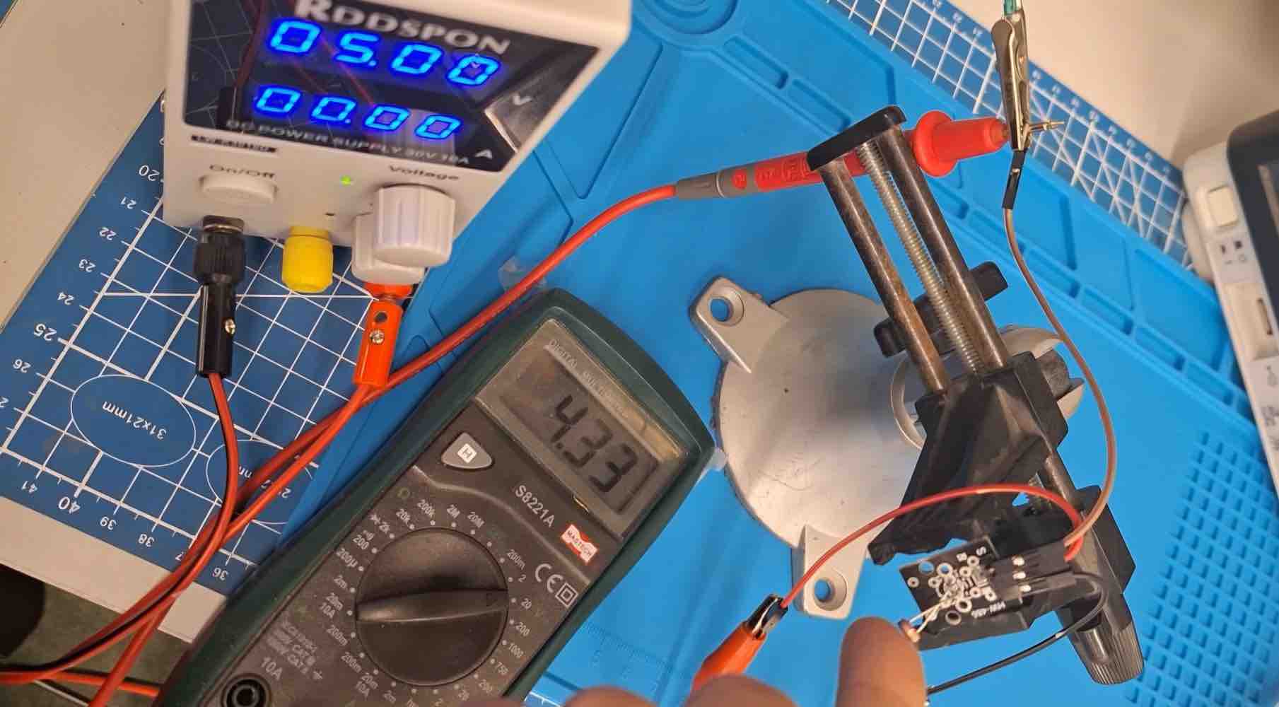
01 | Multimeter on the photoresistor's AO pin. Set to DC voltage, we probed the analog-out pin while changing how much light hit the sensor. The reading changed continuously:
- Normal room light: ~2.88 V
- Sensor fully covered (darkness): ~4.3 V
- Bright light directly on the sensor: ~1.13 V
02 | Oscilloscope on the same AO pin. Moved the probe from the multimeter to the scope (1 V / division). Waving a hand over the photoresistor produced a smooth, continuously-changing wave on screen — visual confirmation that the photoresistor's output is an analog wave, not a sequence of discrete states.
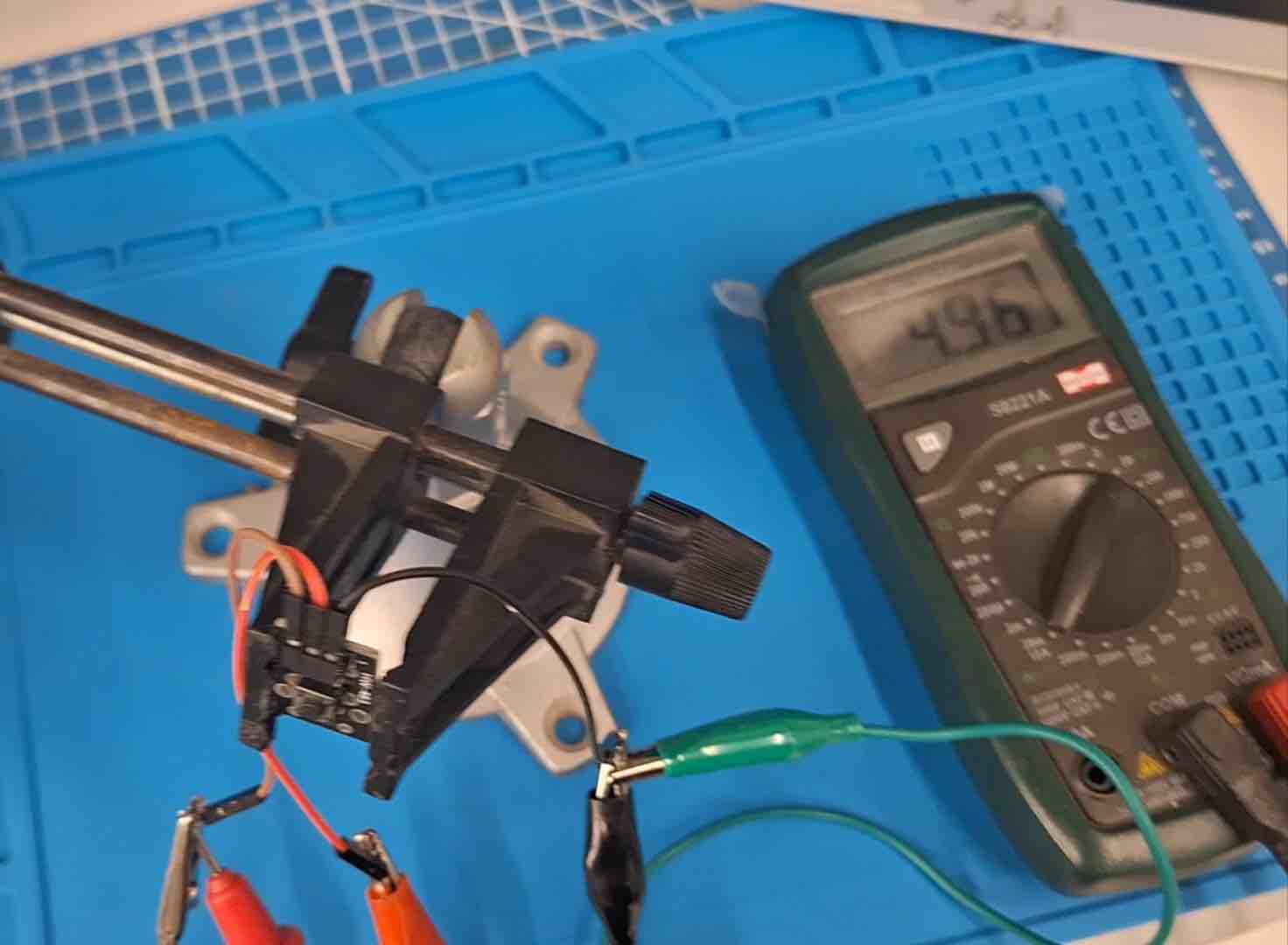
02: Probing a digital signal — push button
digitalRead() / pin.value() here, not analogRead().
Side-by-side conclusion: the photoresistor's output is a continuous wave — every brightness has its own voltage. The push-button's output is binary with a sharp threshold — pressed or not, nothing in between. The probing setup (power supply + multimeter + scope) is identical; what changes is the nature of the signal coming out of the sensor.
- Feedback: Seeing analog vs digital side-by-side made the rest of the input-devices week click. The final project uses an MPU6050 — which is sort of both: an analog quantity (acceleration) sampled by the chip's internal ADC and exposed over I²C as digital words. Understanding that the underlying physics is continuous (like the photoresistor) but the data we read in MicroPython is already digitised (like the push button) is exactly the mental model I needed to set up the calibration baseline correctly.
- Challenge: As a remote student joining from Kuwait while the bench was in Saudi Arabia, I couldn't drive the multimeter / scope probes myself — I had to follow what the in-lab team was doing on screen and ask for re-shots. The next step for me is to repeat this side-by-side test locally once my own equipment arrives, this time on the MPU6050 (probing the I²C lines on the scope) so I can see the actual SDA/SCL clocking pattern.
Individual assignment:
01: Add a sensor to a microcontroller board that you have designed and read it
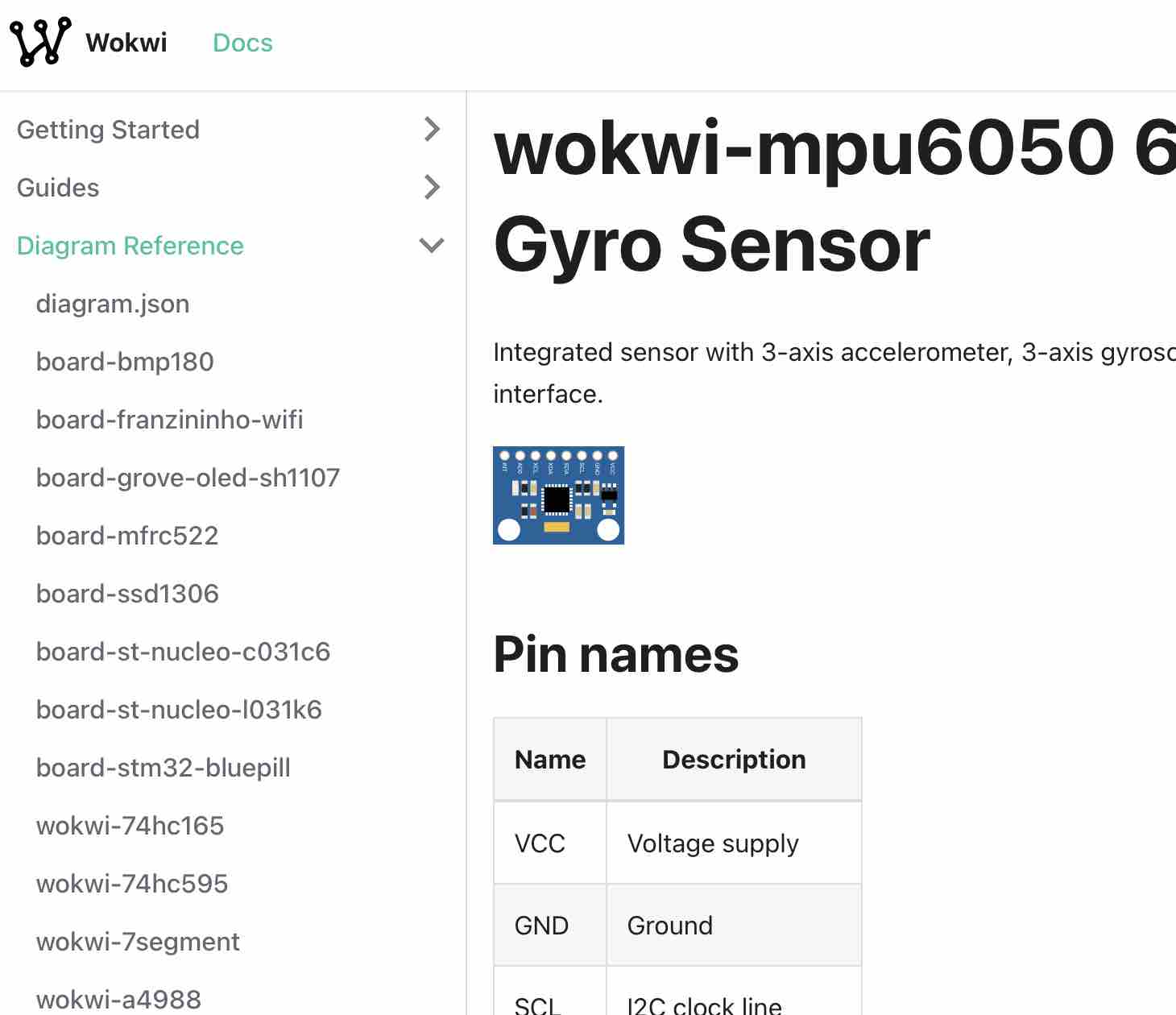
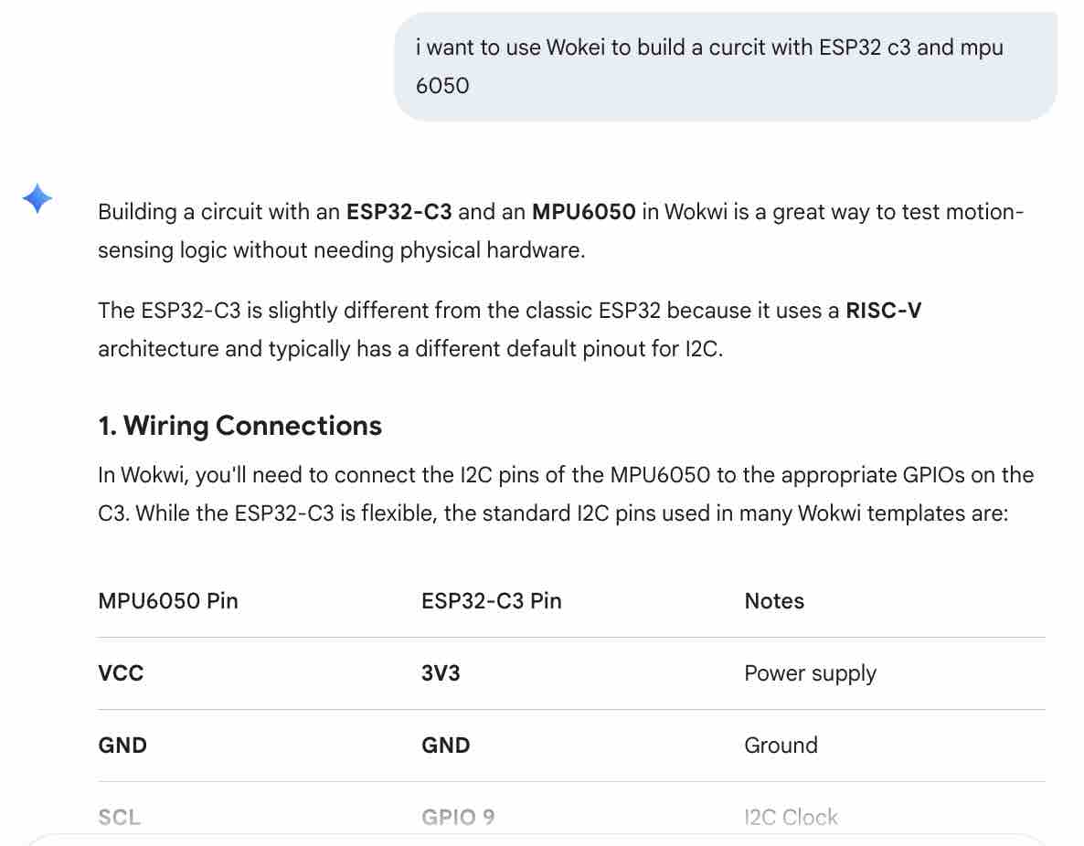
01 | I used an MPU6050 GY-521, which is also part of my final project. I learned all the information I needed from Wokwi and started a virtual simulation, as I was away from the lab and wanted to utilize my time to start this assignment.
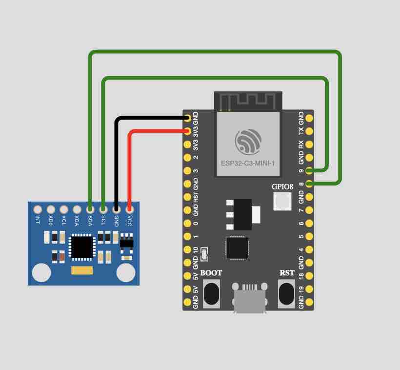
02| I built the circuit connecting the MPU to the ESP32 C3
03| From Gemini AI I got some guidelines on how to continue the process
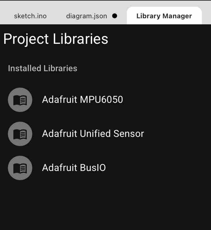
04| I added these libraries
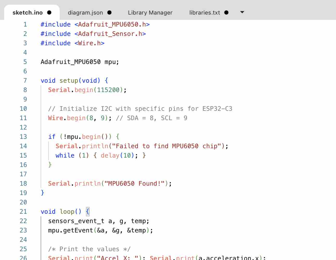
05| and I included
#include <Adafruit_MPU6050.h>
#include <Adafruit_Sensor.h>
#include <Wire.h>

Adafruit_MPU6050 mpu;

void setup(void) {
  Serial.begin(115200);

  // Define I2C pins for ESP32-C3 (SDA=8, SCL=9)
  Wire.setPins(8, 9);

  if (!mpu.begin()) {
    Serial.println("Failed to find MPU6050 chip");
    while (1) { delay(10); }
  }

  Serial.println("MPU6050 Found!");

  // Set sensor ranges (optional)
  mpu.setAccelerometerRange(MPU6050_RANGE_8_G);
  mpu.setGyroRange(MPU6050_RANGE_500_DEG);
  mpu.setFilterBandwidth(MPU6050_BAND_21_HZ);

  delay(100);
}

void loop() {
  sensors_event_t a, g, temp;
  mpu.getEvent(&a, &g, &temp);

  /* Print out the values */
  Serial.print("Accel X: "); Serial.print(a.acceleration.x);
  Serial.print(", Y: "); Serial.print(a.acceleration.y);
  Serial.print(", Z: "); Serial.print(a.acceleration.z);
  Serial.println(" m/s^2");

  delay(500);
}
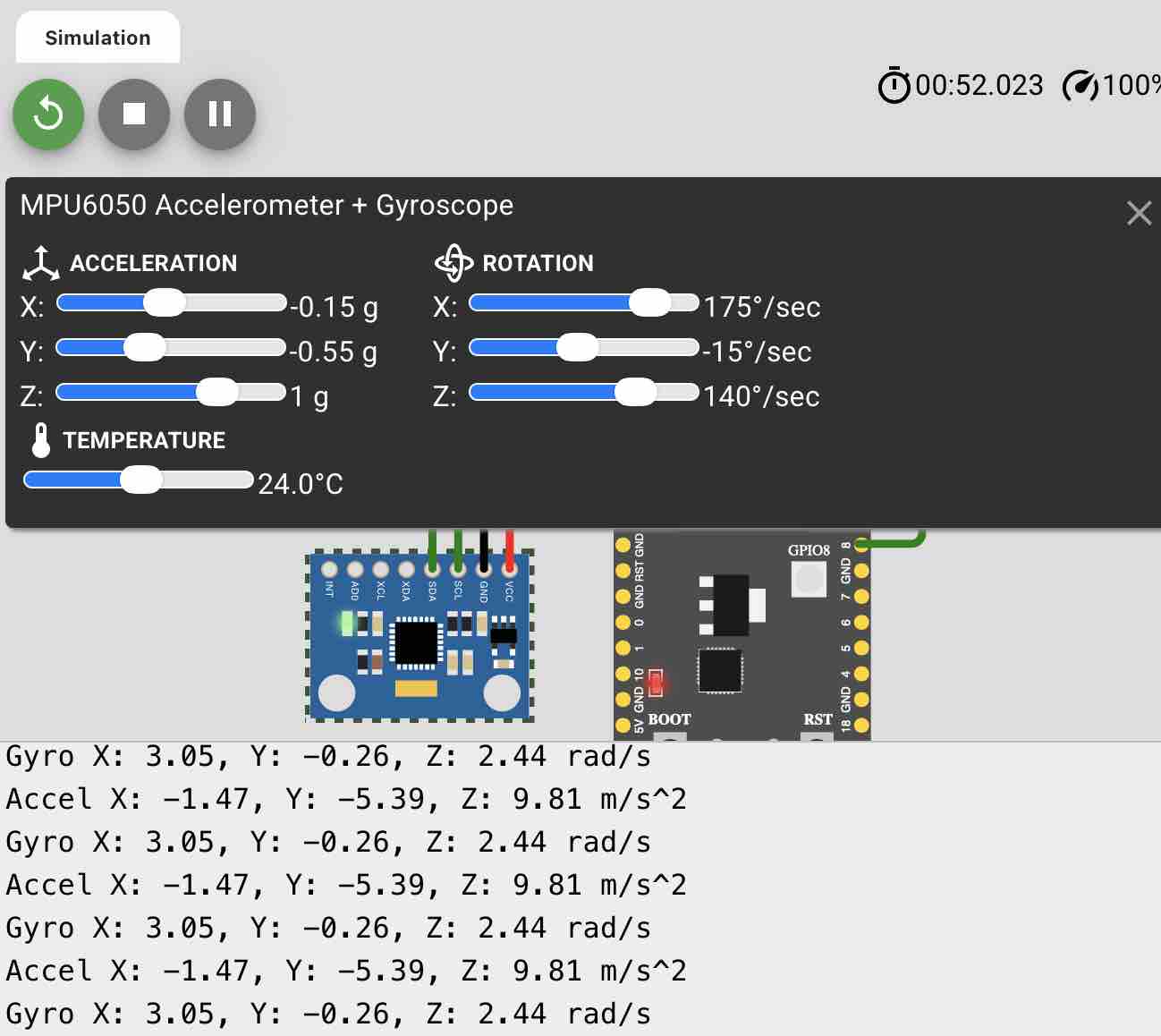
06| I started the simulation, watched the readings come in, and changed the values to see how the sensor responded.
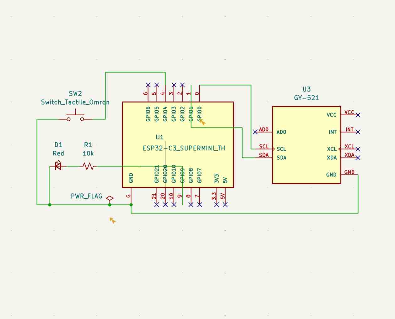
07| Then I opened my KiCad file in the schematic editor and added the GY-521 as a sensor and made the connections, following this workflow: Look for part → not available → search on SnapEDA → download symbol & footprint → open KiCad → import the library → add the new part → connected pins → mark other pins as "no connect" → run ERC
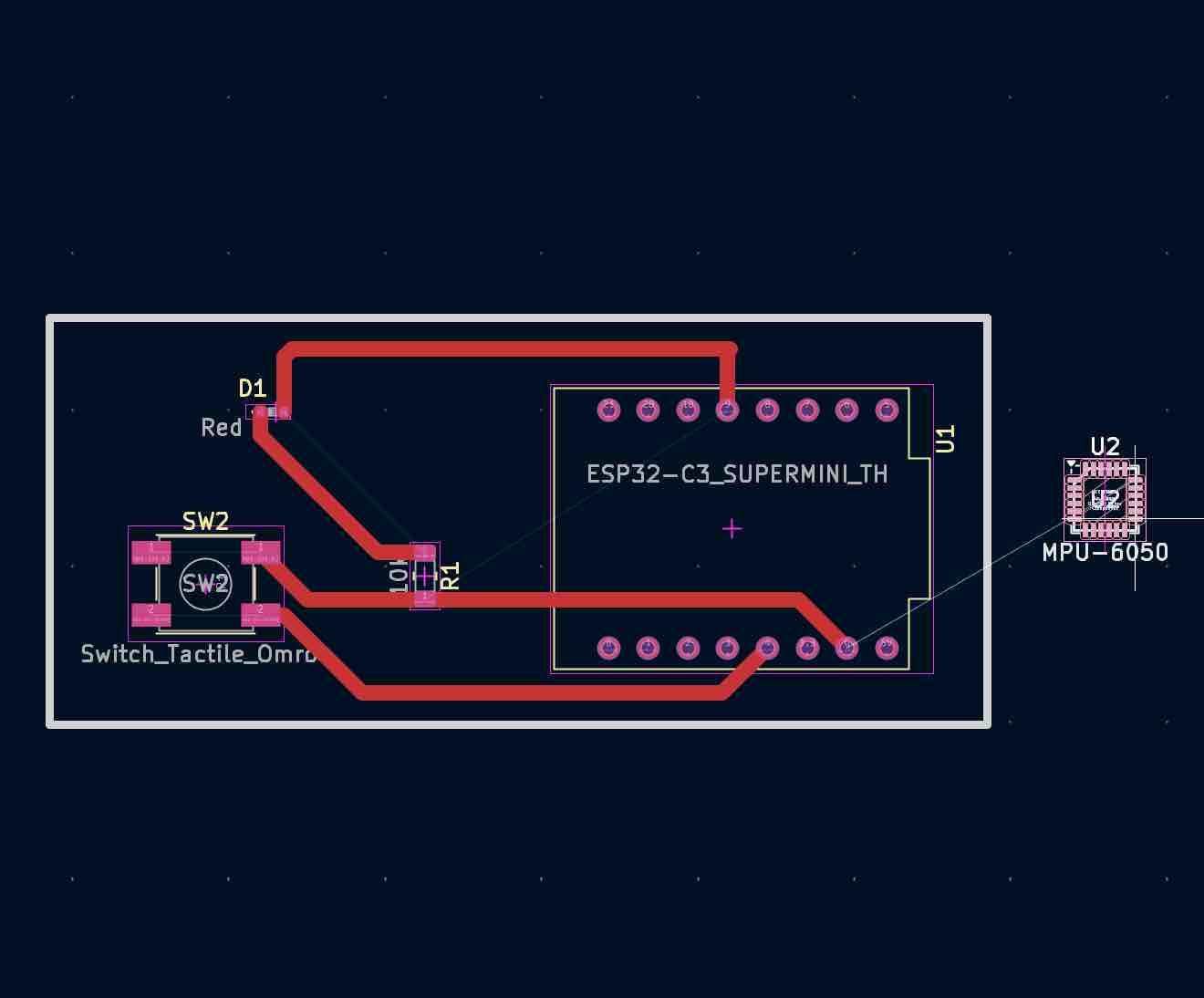
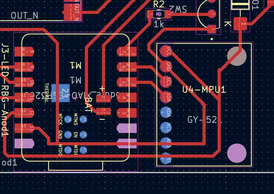
08| Then I updated the PCB Editor and placed the new input sensor
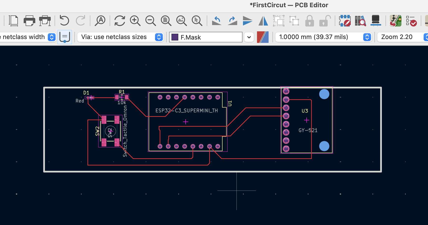
09| I tried to place it next to the microcontroller so that my full design fits on a 30mm copper tape, which I have access to cut for the circuit.
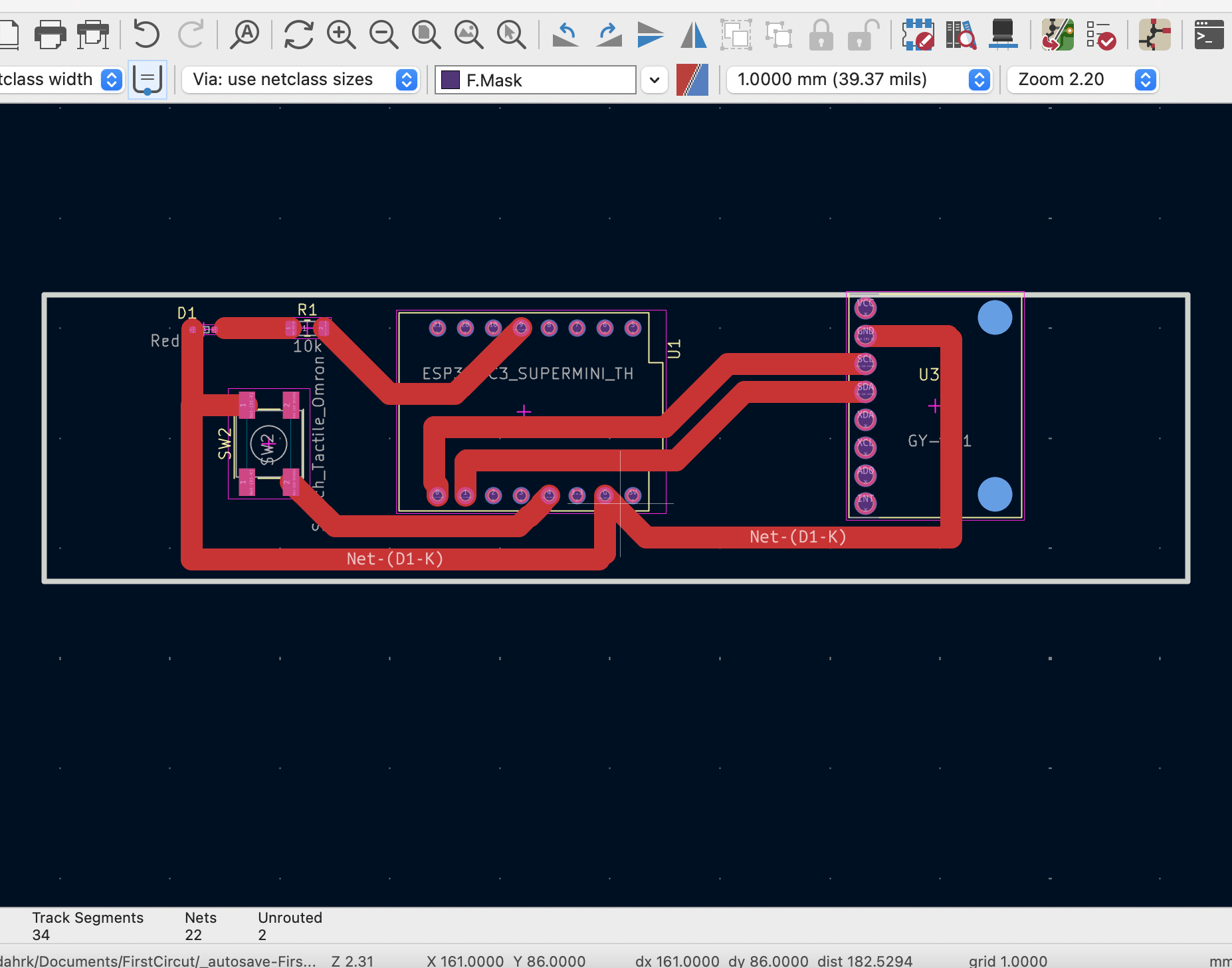
10| For better cutting results, I made the routes 2mm wide and made sure there was enough space between them to avoid short circuits
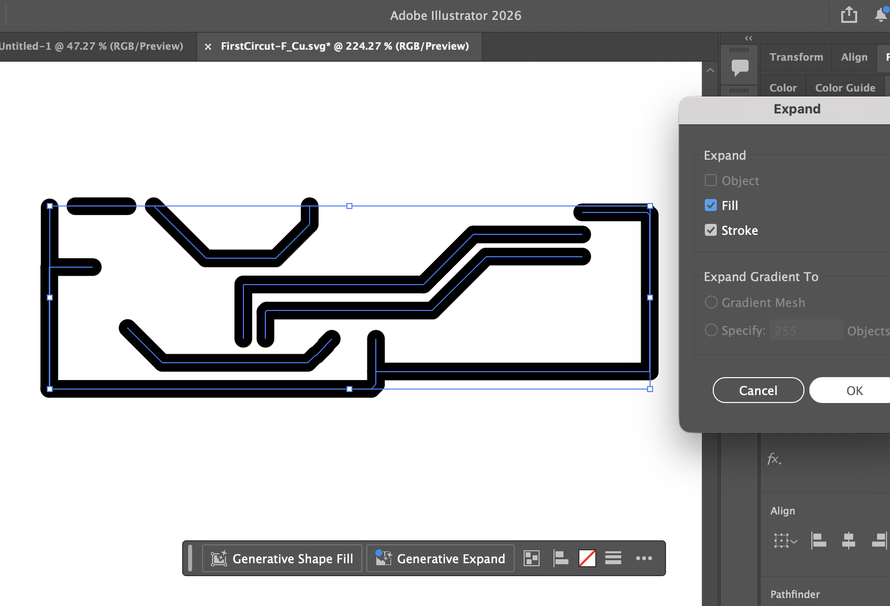
11| From KiCad, I plotted the PCB as SVG → imported it to Adobe Illustrator → transformed it to shape → selected all shapes → created a union → exported as SVG → imported to Cutting Studio → cut the circuit on copper tape.
12| This is how the circuit looks after cutting
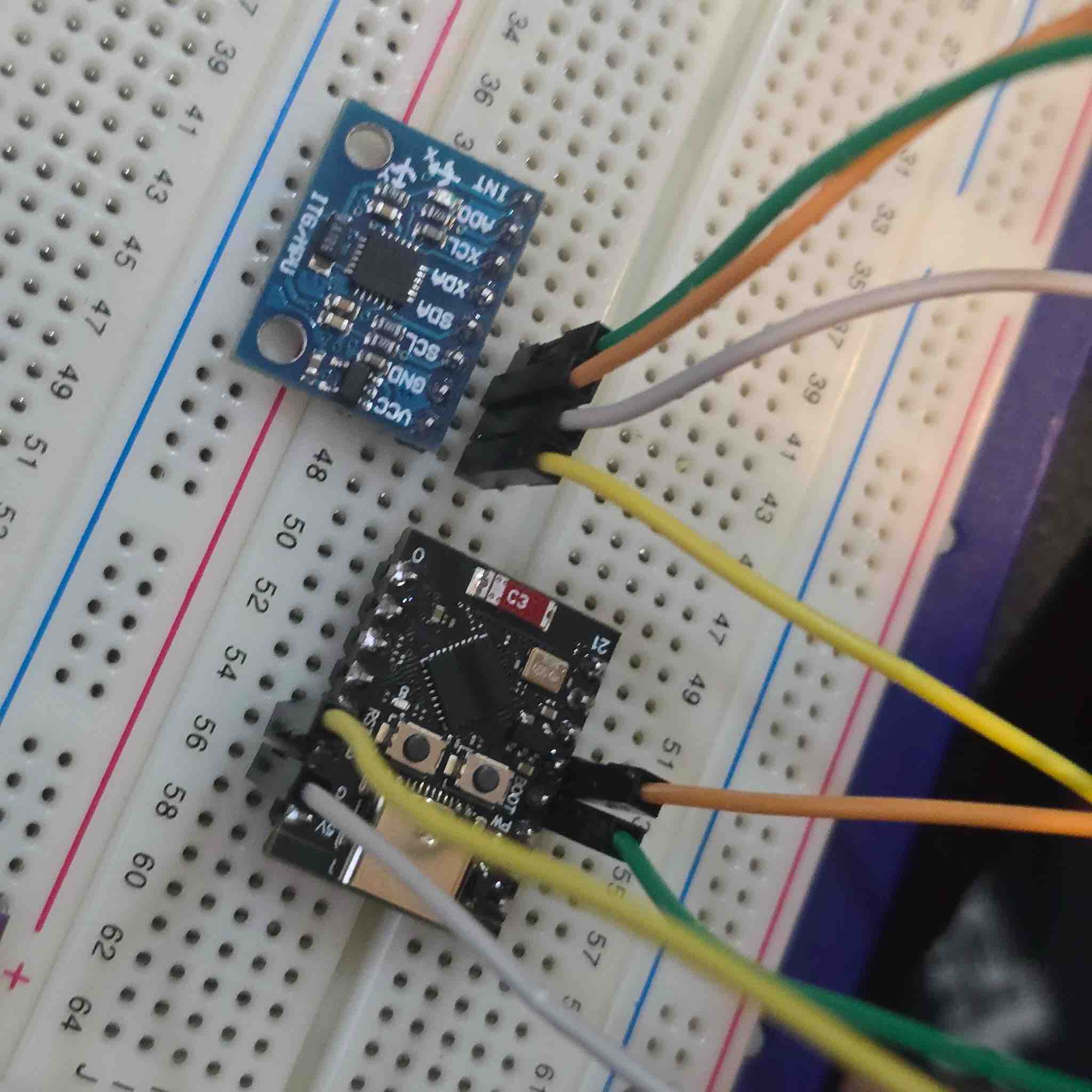
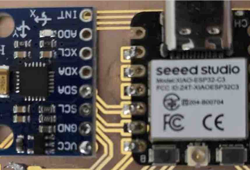
13| Here, I connected the MPU to the ESP32 using a breadboard
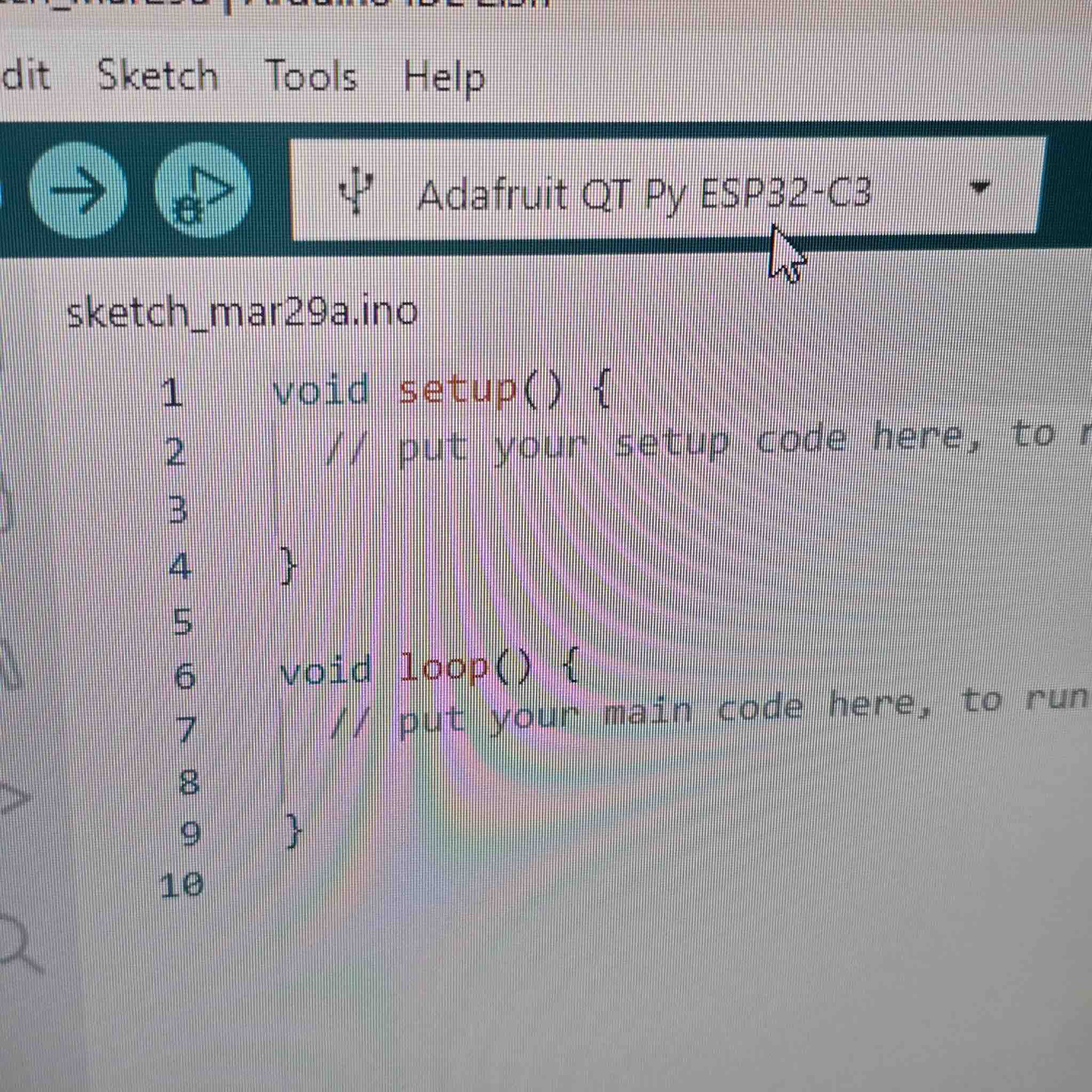
14| I use Arduino IDE to program the ESP32 C3, and I made sure I had the library selected
13| I added , which was used in the simulation in step 5
#include <Adafruit_MPU6050.h>
#include <Adafruit_Sensor.h>
#include <Wire.h>

Adafruit_MPU6050 mpu;

void setup(void) {
  Serial.begin(115200);

  // Define I2C pins for ESP32-C3 (SDA=8, SCL=9)
  Wire.setPins(8, 9);

  if (!mpu.begin()) {
    Serial.println("Failed to find MPU6050 chip");
    while (1) { delay(10); }
  }

  Serial.println("MPU6050 Found!");

  // Set sensor ranges (optional)
  mpu.setAccelerometerRange(MPU6050_RANGE_8_G);
  mpu.setGyroRange(MPU6050_RANGE_500_DEG);
  mpu.setFilterBandwidth(MPU6050_BAND_21_HZ);

  delay(100);
}

void loop() {
  sensors_event_t a, g, temp;
  mpu.getEvent(&a, &g, &temp);

  /* Print out the values */
  Serial.print("Accel X: "); Serial.print(a.acceleration.x);
  Serial.print(", Y: "); Serial.print(a.acceleration.y);
  Serial.print(", Z: "); Serial.print(a.acceleration.z);
  Serial.println(" m/s^2");

  delay(500);
}
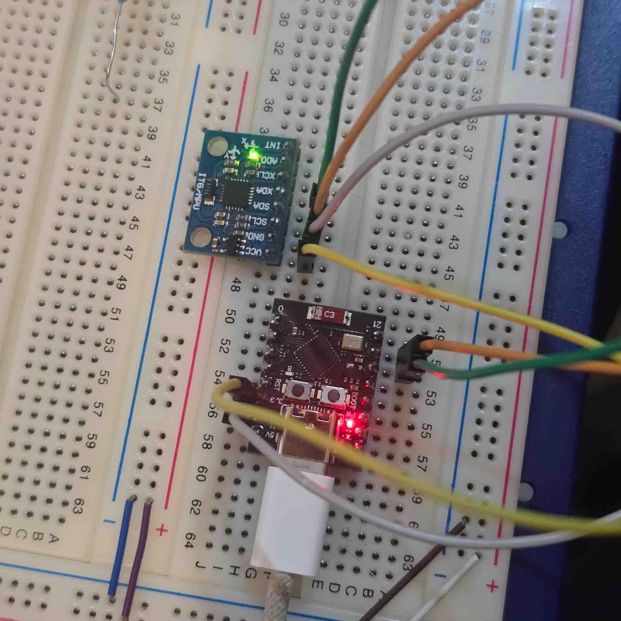
16| I connected the USB to the ESP to start downloading the program
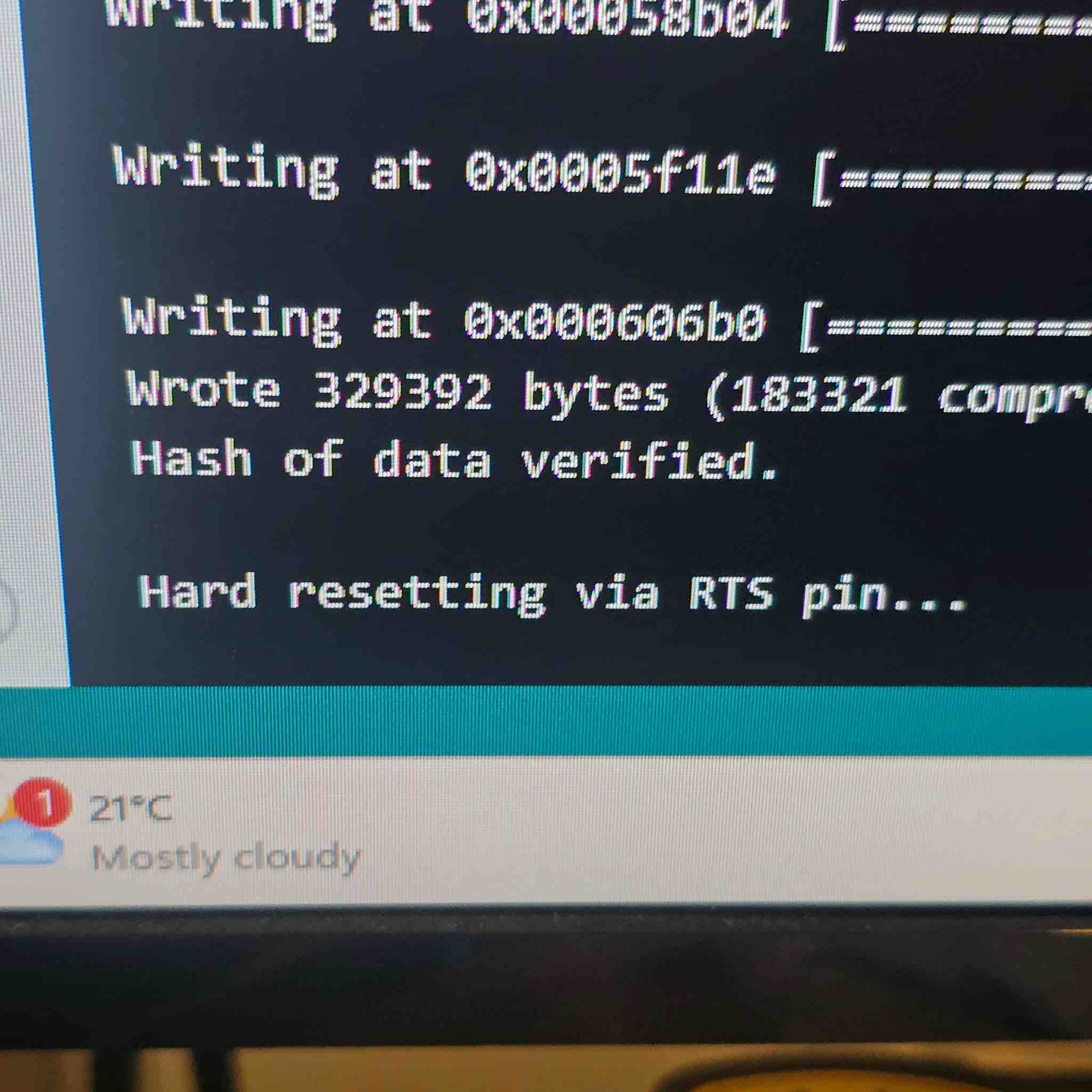
17| I had to reset the microcontroller by pressing the button
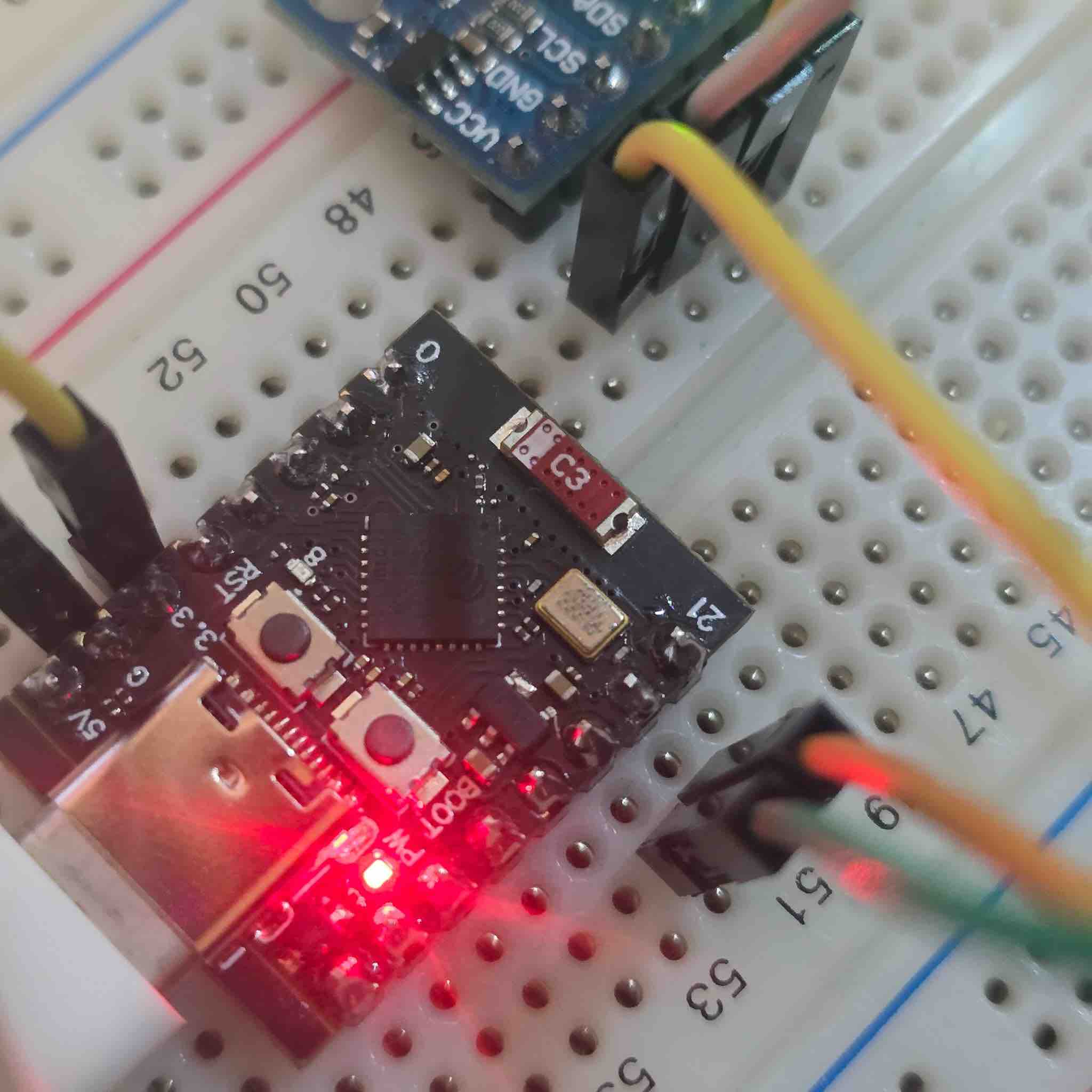
18| This is the button I pressed, and after a few minutes I got the following reading in the IDE
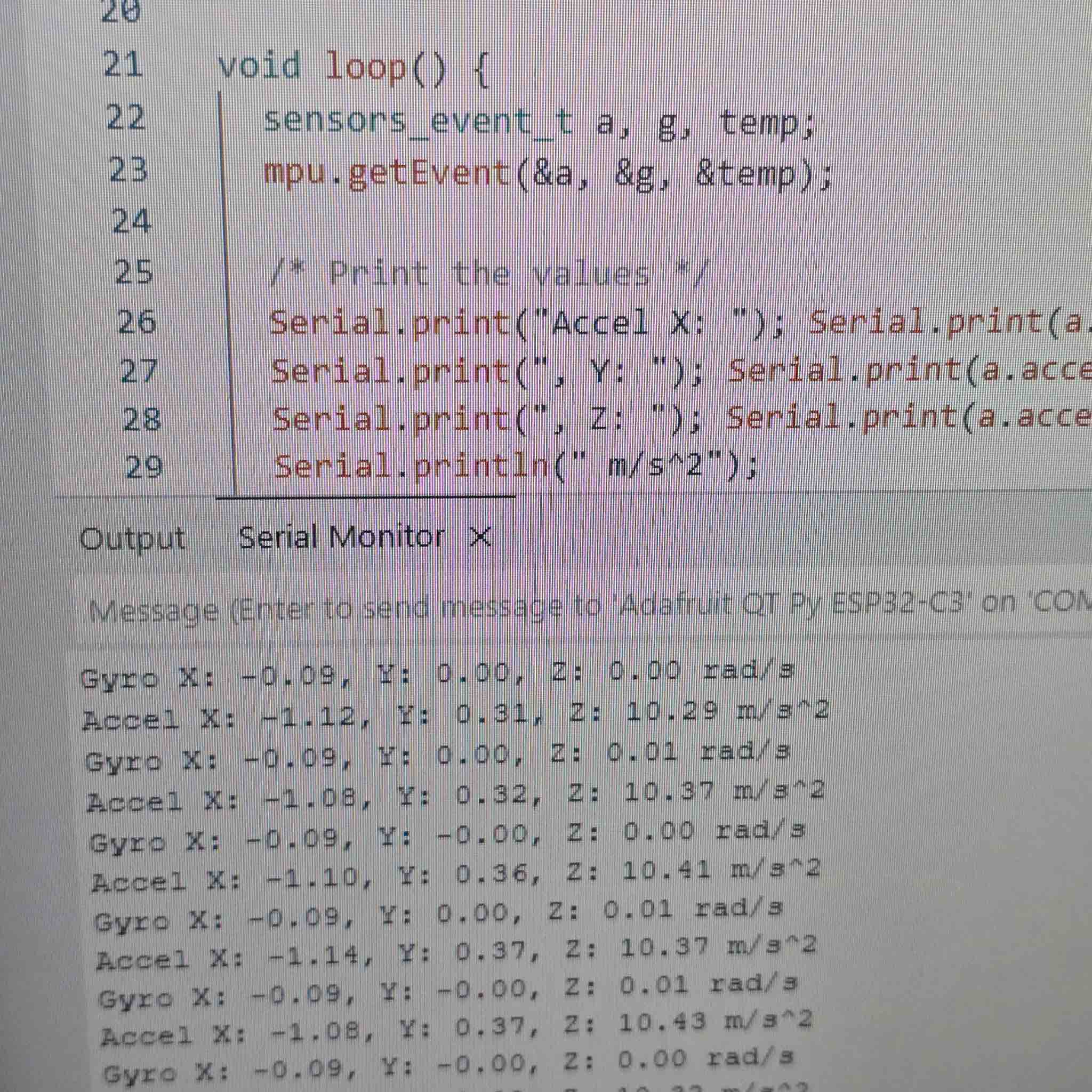
19| The readings of x, y, z axes as well as the acceleration of change. To make a better visual, I needed to plot these values on a chart
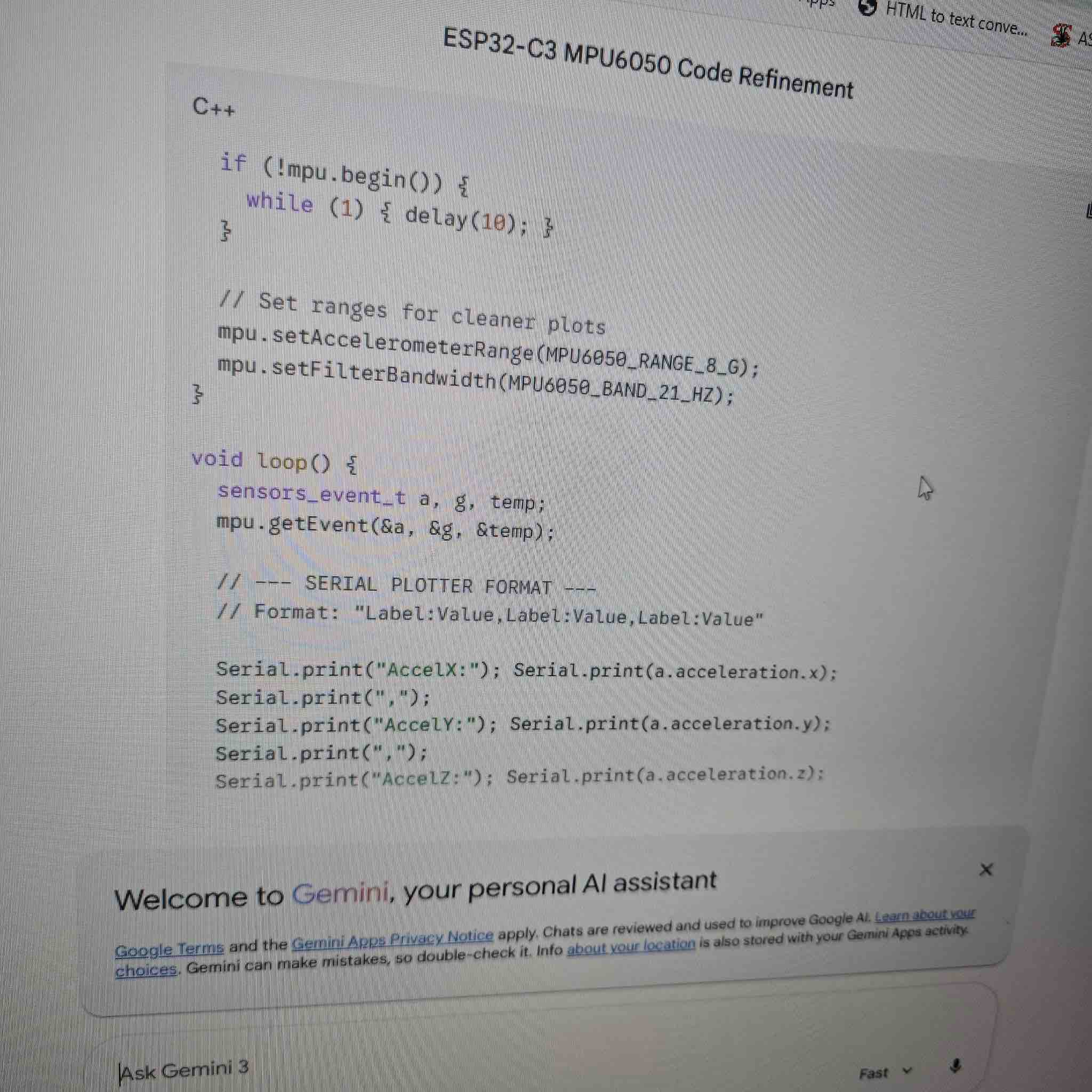
20| For that, I had to add a plotting command to my code, and I used Gemini to redefine the code to
// --- SERIAL PLOTTER FORMAT ---
// Format: "Label:Value,Label:Value,Label:Value"

  Serial.print("AccelX:"); Serial.print(a.acceleration.x);
  Serial.print(",");
  Serial.print("AccelY:"); Serial.print(a.acceleration.y);
  Serial.print(",");
  Serial.print("AccelZ:"); Serial.print(a.acceleration.z);
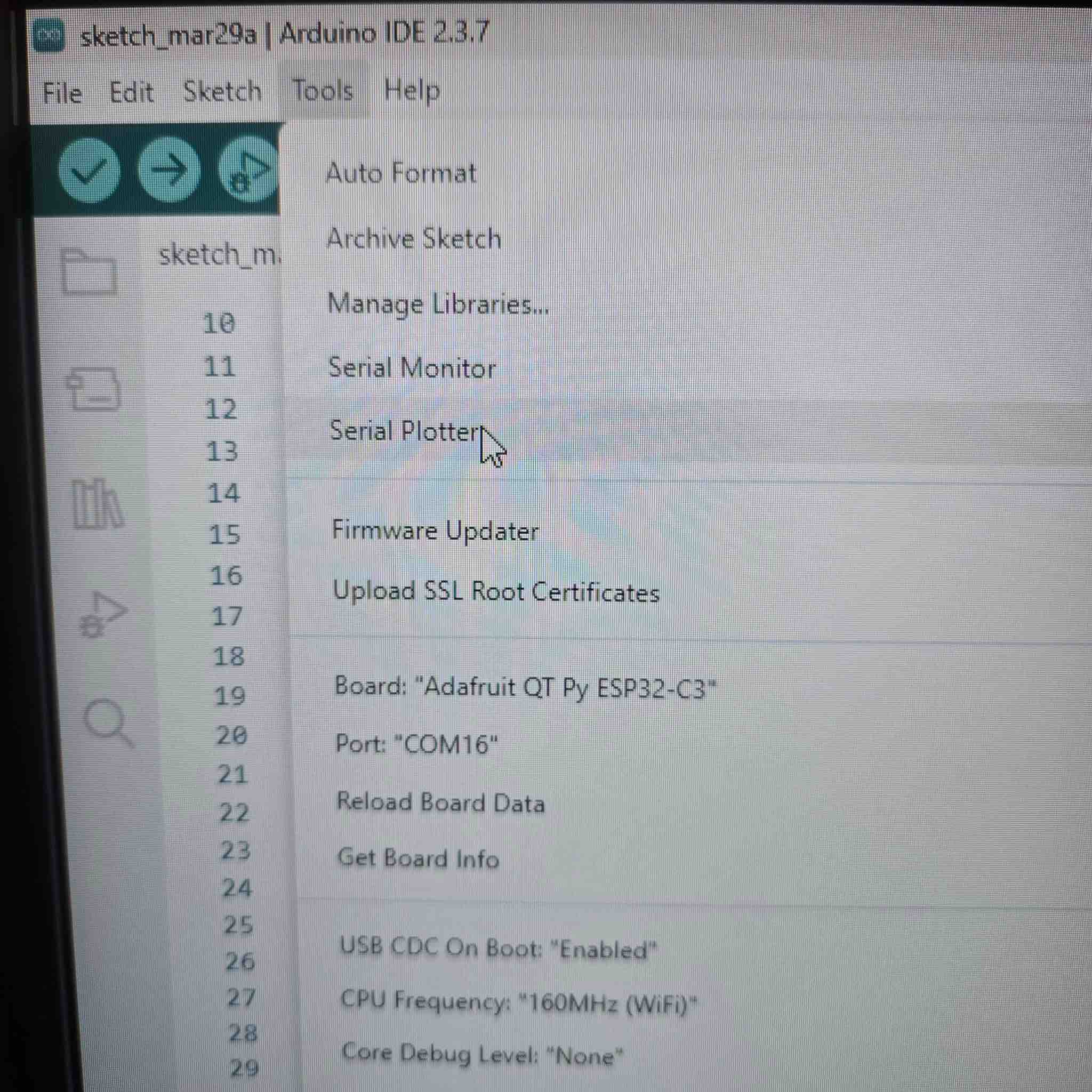
21| After re-downloading the new program to the microcontroller, I went to Tools → Serial Plotter
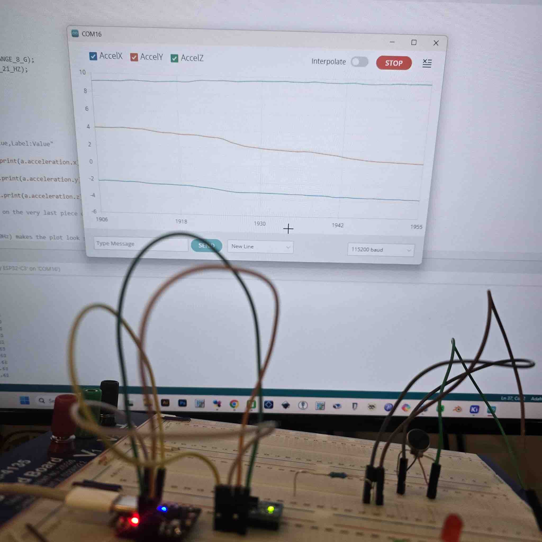
22| And I started to get the readings from the sensor in the graph
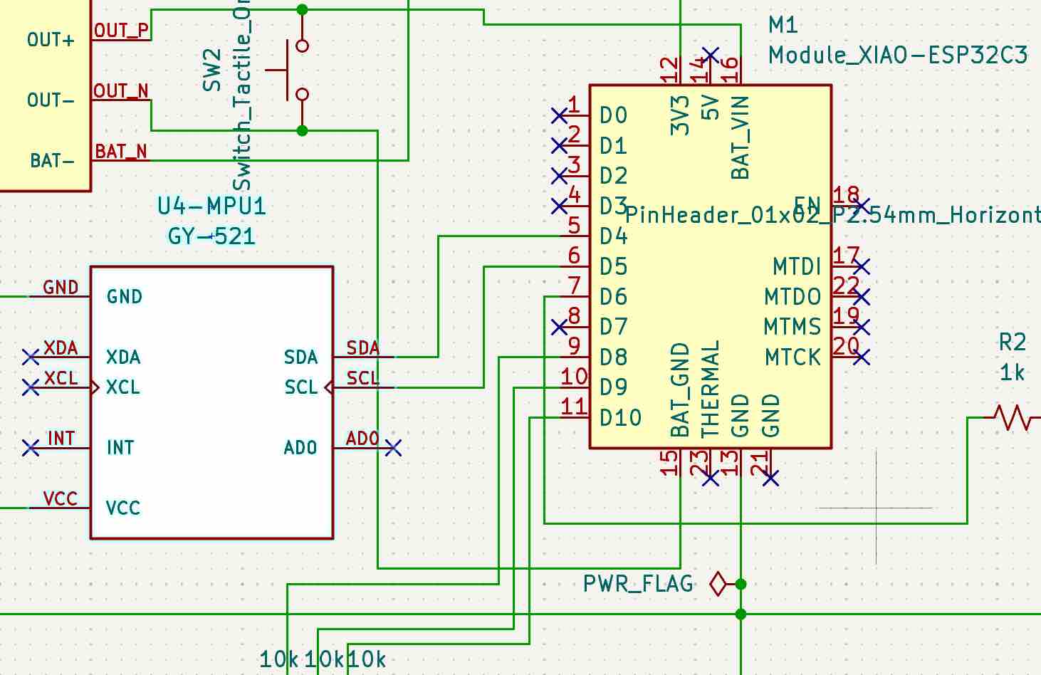
23| Now I was ready to add my MPU to the PCB, solder it, and test. I changed the microcontroller and updated the schematic, keeping the same pins connected.
24| Reconnected the routes and tracks for my final project. To bridge over other pins on the PCB, I added tape to create an isolated layer — the same trick I used in Week 08 — Electronics Production.
25| Even though the MPU has through-hole pins, I used them as SMD pads. I put a little solder on each pad before placing the MPU; after placing it, I added a little more solder into the holes and held the iron tip on the joint to give the two pieces of solder a chance to melt and merge. Then I added more solder as needed and kept checking connectivity with a multimeter.
26| I developed the code with the help of Gemini to read the different values when tilting the MPU —
# MPU sensor and reading
import machine
import time
import struct

# Initialize I2C
i2c = machine.I2C(0, sda=machine.Pin(6), scl=machine.Pin(7))
addr = 0x68

# IMPORTANT: Wake up the MPU-6050 inside this script
try:
    i2c.writeto_mem(addr, 0x6B, b'\x00')
    print("MPU-6050 Woken Up Successfully")
except:
    print("Could not find sensor. Check wires!")

def read_accel():
    try:
        # Read 6 bytes starting from 0x3B
        data = i2c.readfrom_mem(addr, 0x3B, 6)
        # Unpack high and low bytes into 3 signed integers (x, y, z)
        return struct.unpack('>hhh', data)
    except:
        return None

while True:
    vals = read_accel()
    if vals:
        ax, ay, az = vals
        print("X: {:6d} | Y: {:6d} | Z: {:6d}".format(ax, ay, az))
    else:
        print("Sensor disconnected!")
        break # Exit the loop if the sensor is lost

    time.sleep(0.2)
- Feedback: I'm very comfortable with the workflow I'm following. There might be easier steps, but I guess this is more of a spiral development with lower risk of errors: simulation → schematic design → PCB design → breadboard unit build → testing → cutting PCB → soldering → final testing → completing.
- Challenge: I cannot be in the lab all the time, so the virtual simulation and finalizing the work on the laptop until I reach the lab is both helpful and uncertain — it all depends on my research and hypothesis, and might lead me to repeat all the work again.