add an output device to a microcontroller board you've designed, and program it to do something
For this week, I will be working on the following components that will be included in my final project:
Mini MP3 Player
Neopixel Led Board
Group Assignment
Again, I am remote and have been working on my group projects alone. I used a multimeter to measure the voltage of the Neopixel component from a strip. It was actually quite interesting, in that the board "datasheet" https://wiki.seeedstudio.com/XIAO-RP2040 says that the five volt pin provides just 5 volts, but I measured 5.27 volts across the voltage pins of the Jeffuino v2. I suppose a 20% tolerance is acceptable in components. Lesson learned- always measure the voltage, current, resistance or capacitance of components. I measured the voltage across the digital in and digital out pins, which would shift from 1.3 mV to 1.2mv as the neopixel would "breathe". Interesting, in that it shows how the neopixel responds to the voltage across the component.
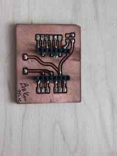
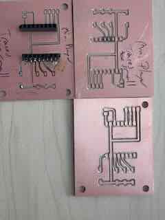
Before I could start testing however, one of the traces on my Jeffuino broke and I had to create a new board. I stripped the old board of components so that I could reuse them.
I had created a new board (see below) based on the datasheet for the neopixels, which recommended a resistor across the data-in line. I added a 330 ohm resistor to a new board, the Jeffuino v.3, but the neopixel wouldn't light using this new board. When I tried to measure the voltage across the resistor from the D6 pin to the neopixel, the LED would light. What I think happened is that the resistor is too high and is filtering out the signal that the Neopixel needs. In practical terms, this will likely mean that I will need to remove the resistor and add a zero ohm resistor as a bridge to make this board functional.
Individual project- Neopixel board
I started out trying to build a modular neopixel pcb board that will allow me to quickly set up and tear down my final project.
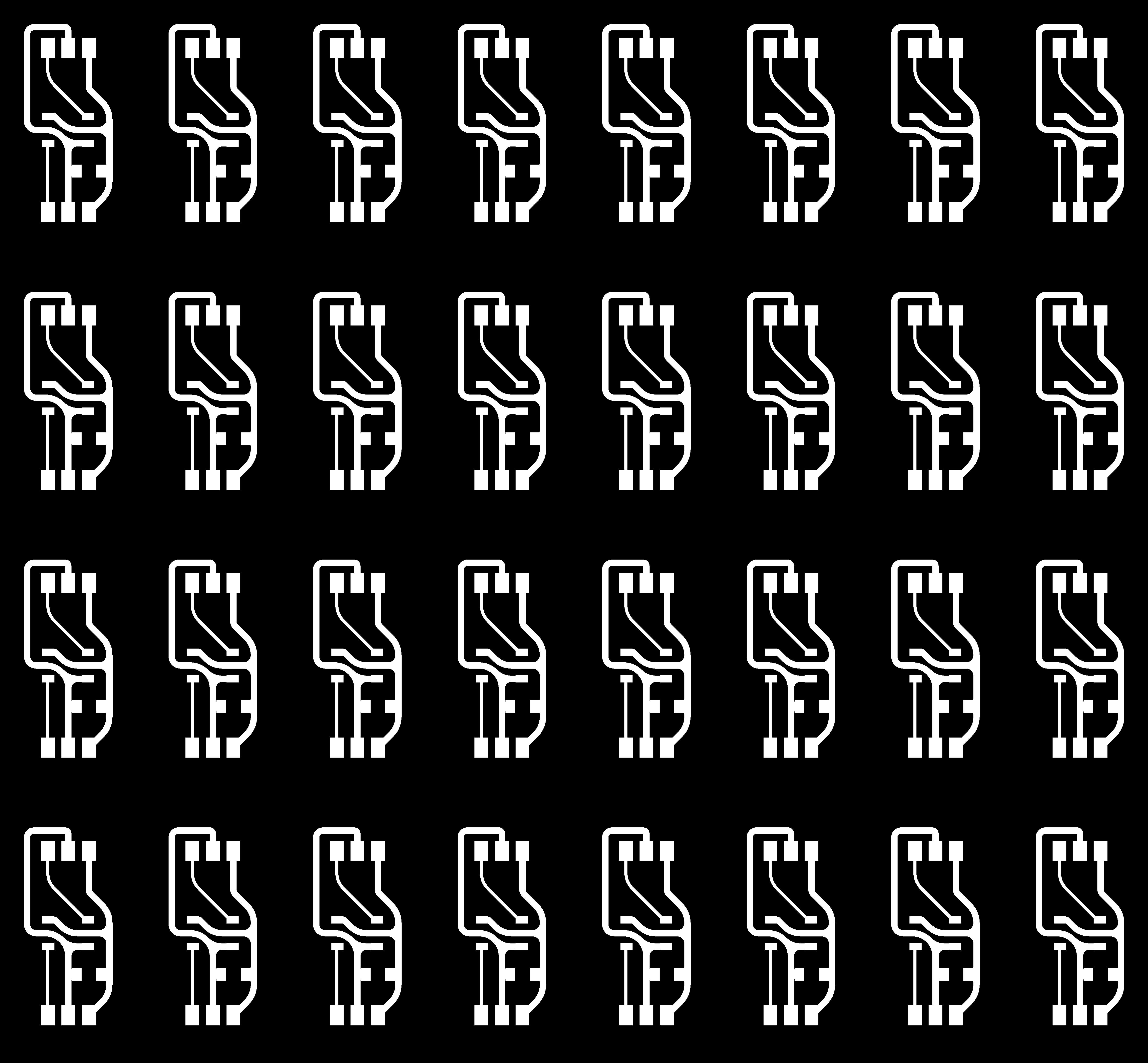
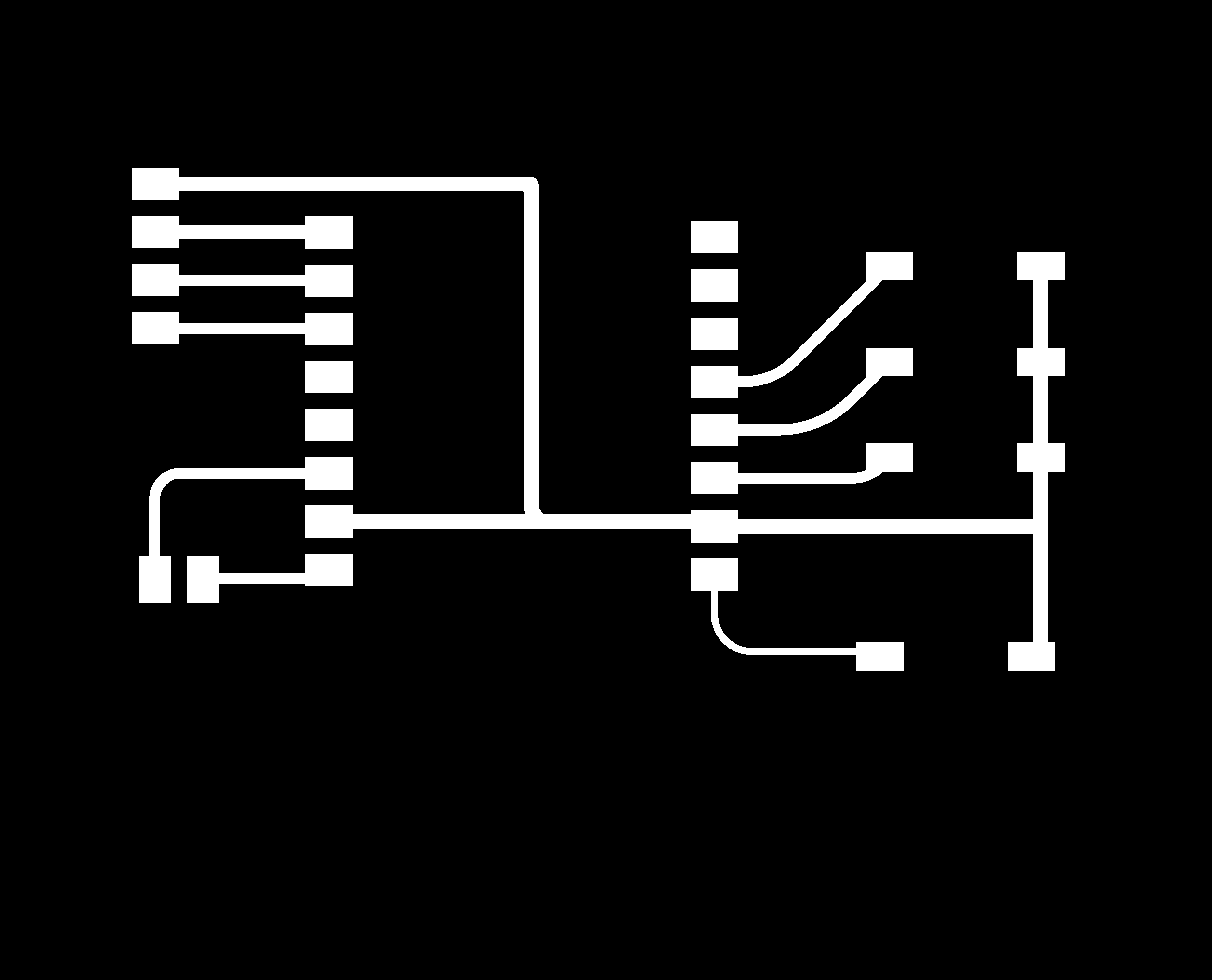
I first started with a prototype board. I removed a neopixel from a strip for this board. The datasheet calls for a 0.07 microfahrad capacitor to connect the voltage and ground. The neopixel has four leads/traces- vss (ground), Digital In, VDD voltage, and Digital out. The traces were really hard to work out given the orientation of the pins on the neopixel. I had added a 0 ohm resistor as a bridge to the board.The schematic is below:
My project will require about 80 of these boards and I figured that I could reduce the cost and time to fabricate if I removed the zero ohm resistor bridge. As part of this project, I will experiment with a batch fabrication workflow to streamline the production of these boards. (More on this later). I revised the board to remove the resistor bridge, the pcb will be round and added mounting holes.
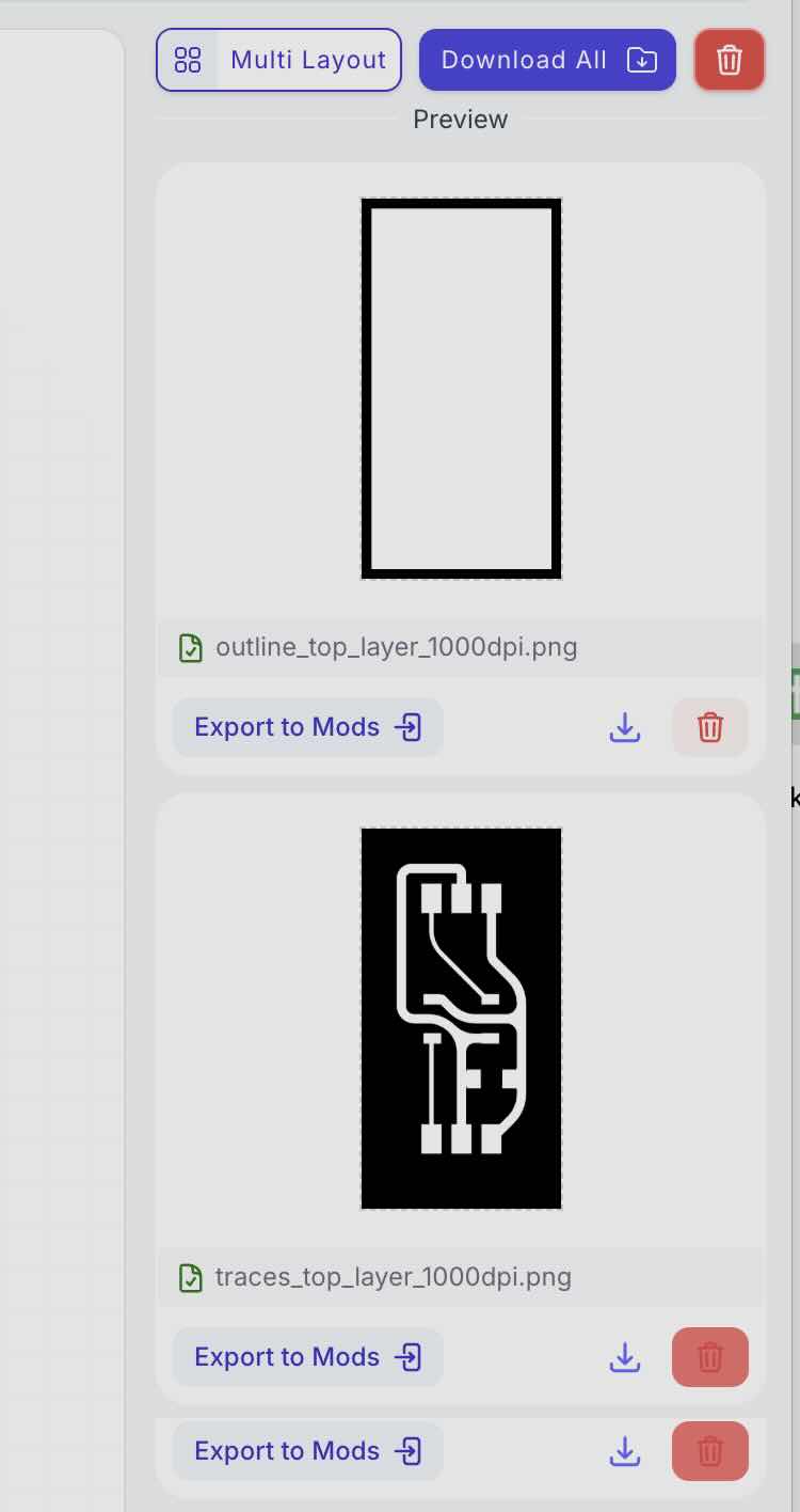
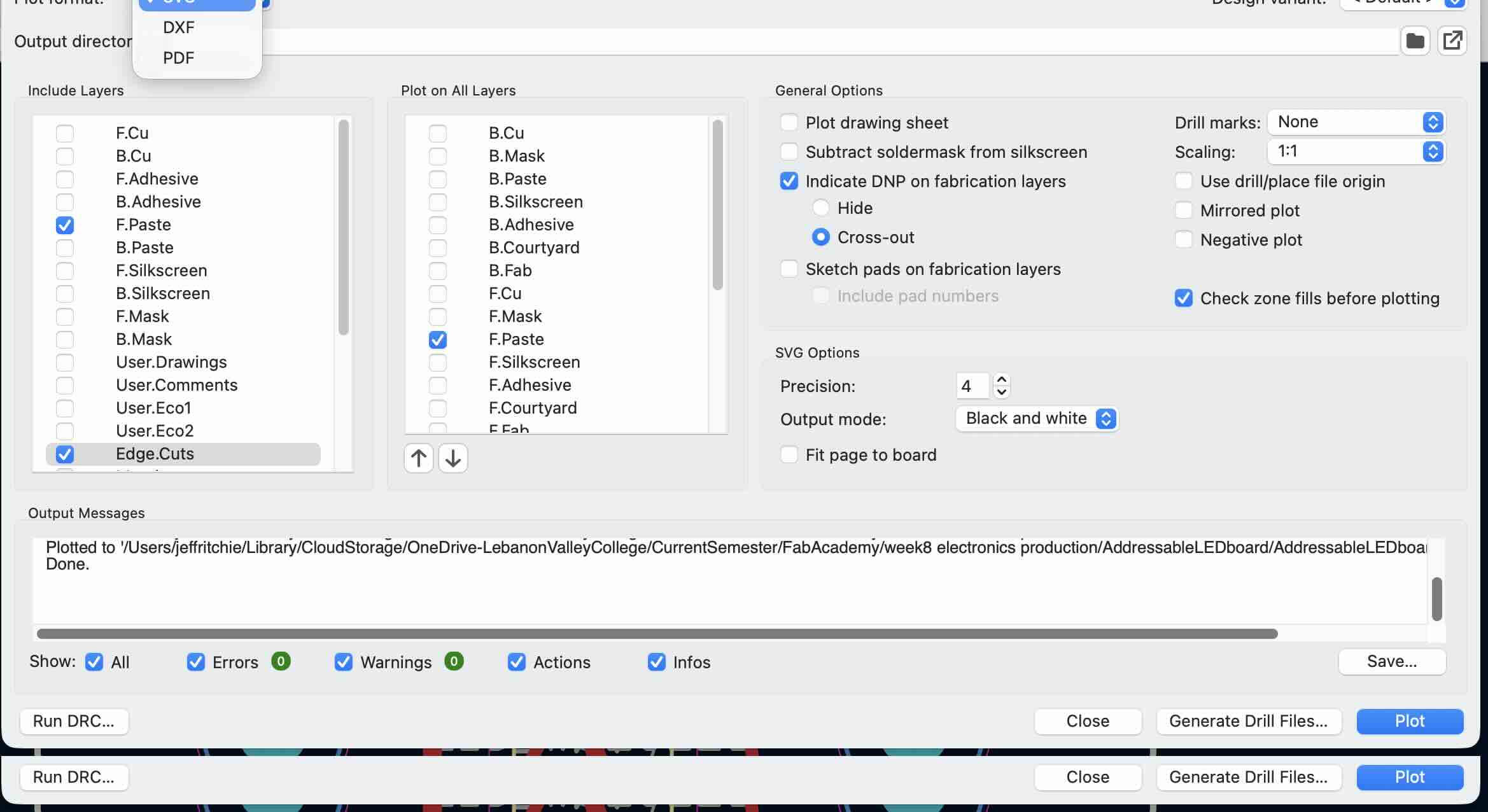
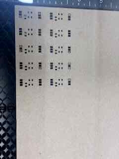
I exported to gerber files, zipped them, and uploaded them to gerber2png. I downloaded the pngs and uploaded them into mods, using the standard/default settings. I used a vbit to cut the traces and then a 1/32 squre end bit to cut the edges.
I hand soldered the board with soldering iron.This proved more difficult than I had thought it would be, with a number of bridges that I needed to fix.
PCB testing
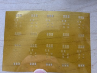
I assembled one pcb to see if the board would work. I hooked it up to my jeffuino and uploaded the following code.
I started out testing continuity and voltage. The Voltage and ground traces were working- the voltage was at 5.27 volts across the led circuit.
My first thought was that I had damaged the LED when I had removed it from an old string.
I tested an existing LED cut from a string and it worked.
I slept on it and the next day I looked at the pinout for the neopixel and compared it to the footprint in the pcb I made, I realized that I had placed the Neopixel on the board in the wrong orientation and had consequently mixed up the traces. This is why it wouldn't work. I attempted to remove the component and reposition it. I had hand soldered the board as I had not assembled the reflow machine, but I think I bridged the solder.
Lessons learned
Double check the data sheets.
Use a multimeter to check continuity in the boards created.
Some chips/components are simply not designed to be hand soldered. I have to get the reflow machine working.
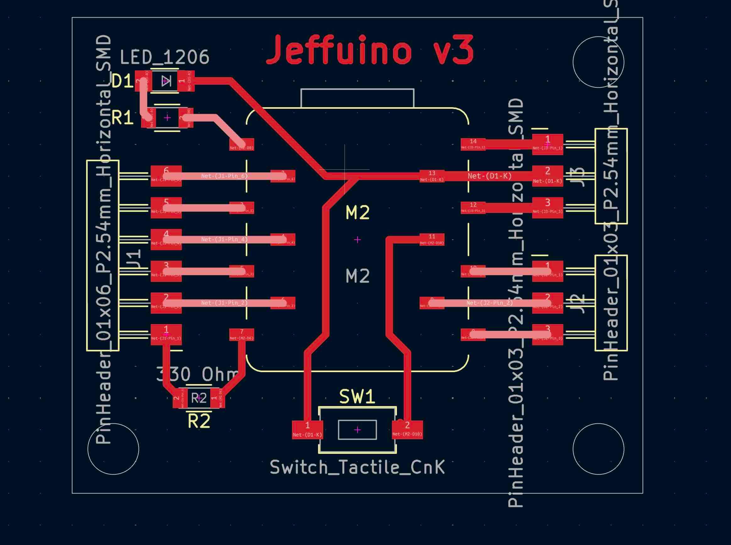
PCB redesign
I change the PCB to reflect larger traces and pads and a screw hole. One thing that I had done in the previous board that was a problem, was that the sequence of in lines (v, g and data) is in a different order than the sequence of out lines. If I want to make this board modular, and make it easier to assemble, I should make input the same sequence as output. That being said, the signal (digital in and out) doesn't have to be run the same as power. I revised the board so that the input and output would be in the same sequence, but in retrospect, the data line doesn't need to run the same as the power in the final project. I also had an issue avoiding bridges when hand soldering.
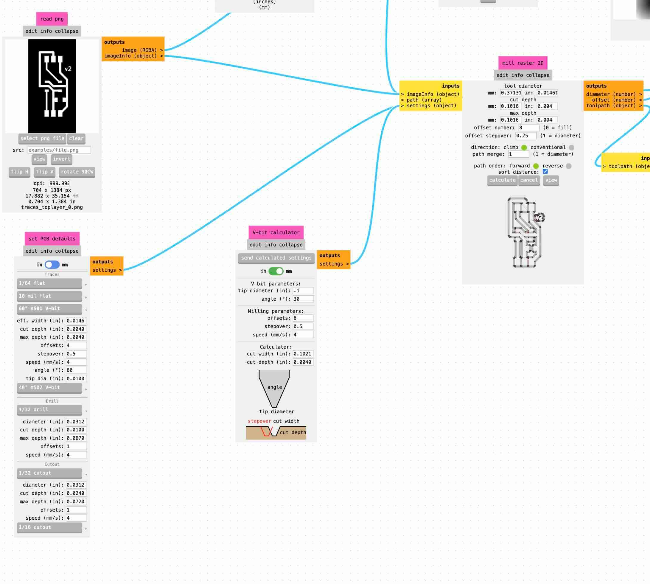
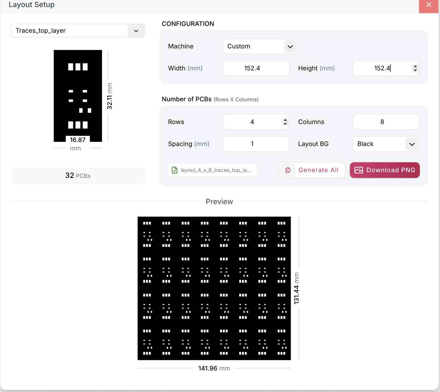
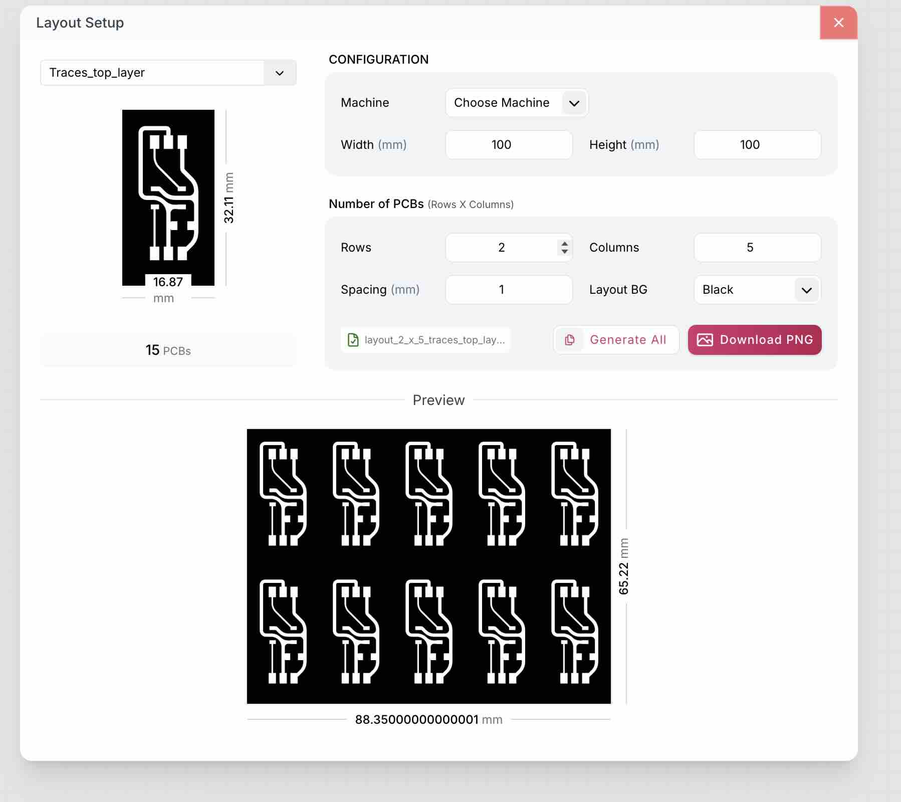
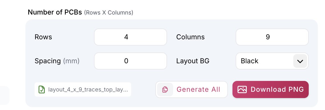
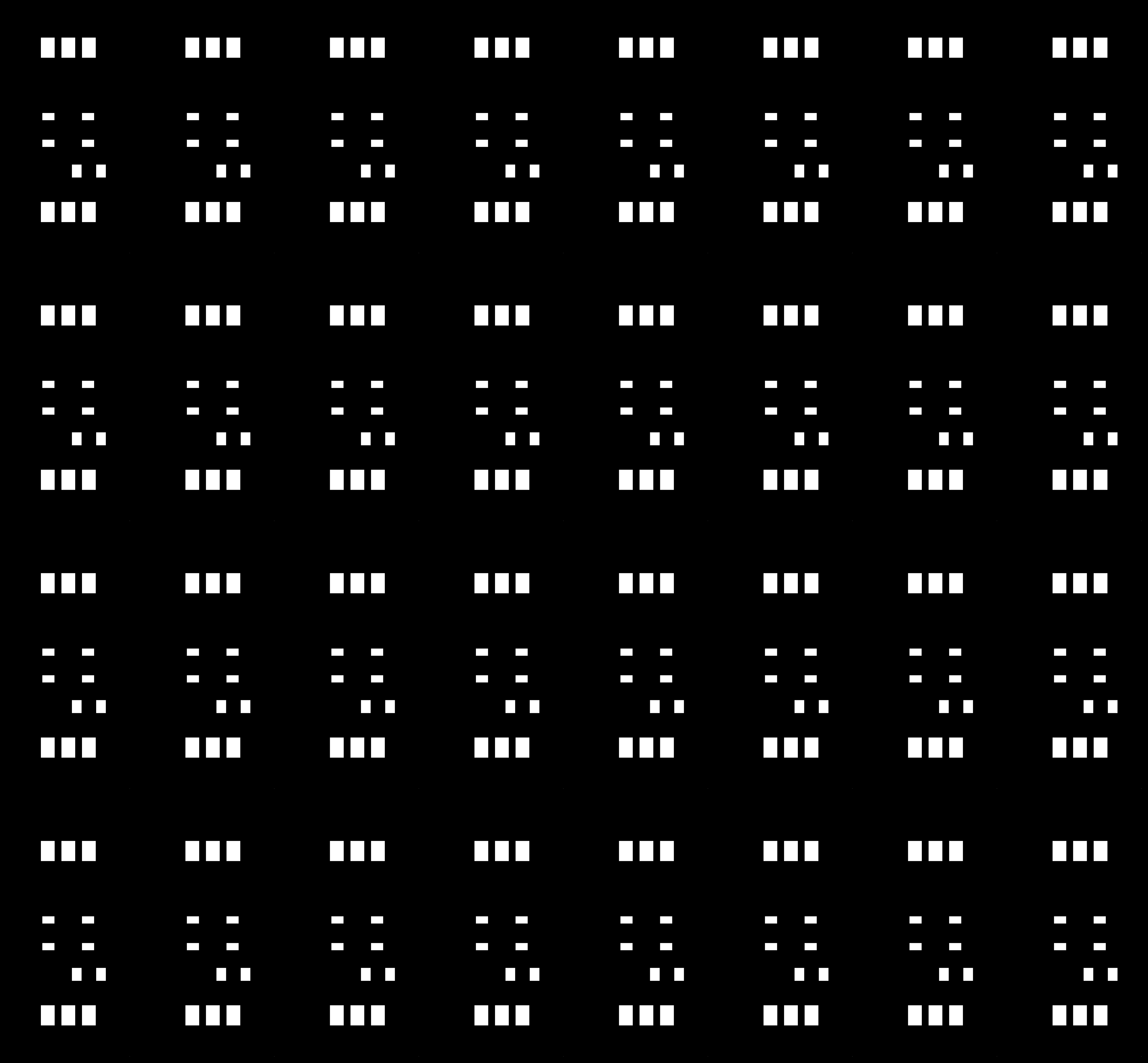
When I fabricated the new Neopixel boards, I experimented with fabricating multiple boards at once (see below) and how I could remove more copper from the boards so that there is less likelihood of shorts. To the latter end, I experimented with offsets, changing the size of the offset number from one to eight and then changed the offset stepover to .25.
The offset stepover is the amount of the bit that the offset takes off- if 1 is the entire diameter of the bit, then .25 would be 1/4. This is helpful in that I can attempt to fabricate finer detail in the PCB and remove more of the copper surrounding the traces to minimize shorts. The downside is that you are not using the entire diameter of the milling bit, which takes longer to remove copper.
I set the number of offsets to 8, which was actually a bad idea as it doubled the time to make each PCB. I need to streamline this process if I am to create 80 boards.
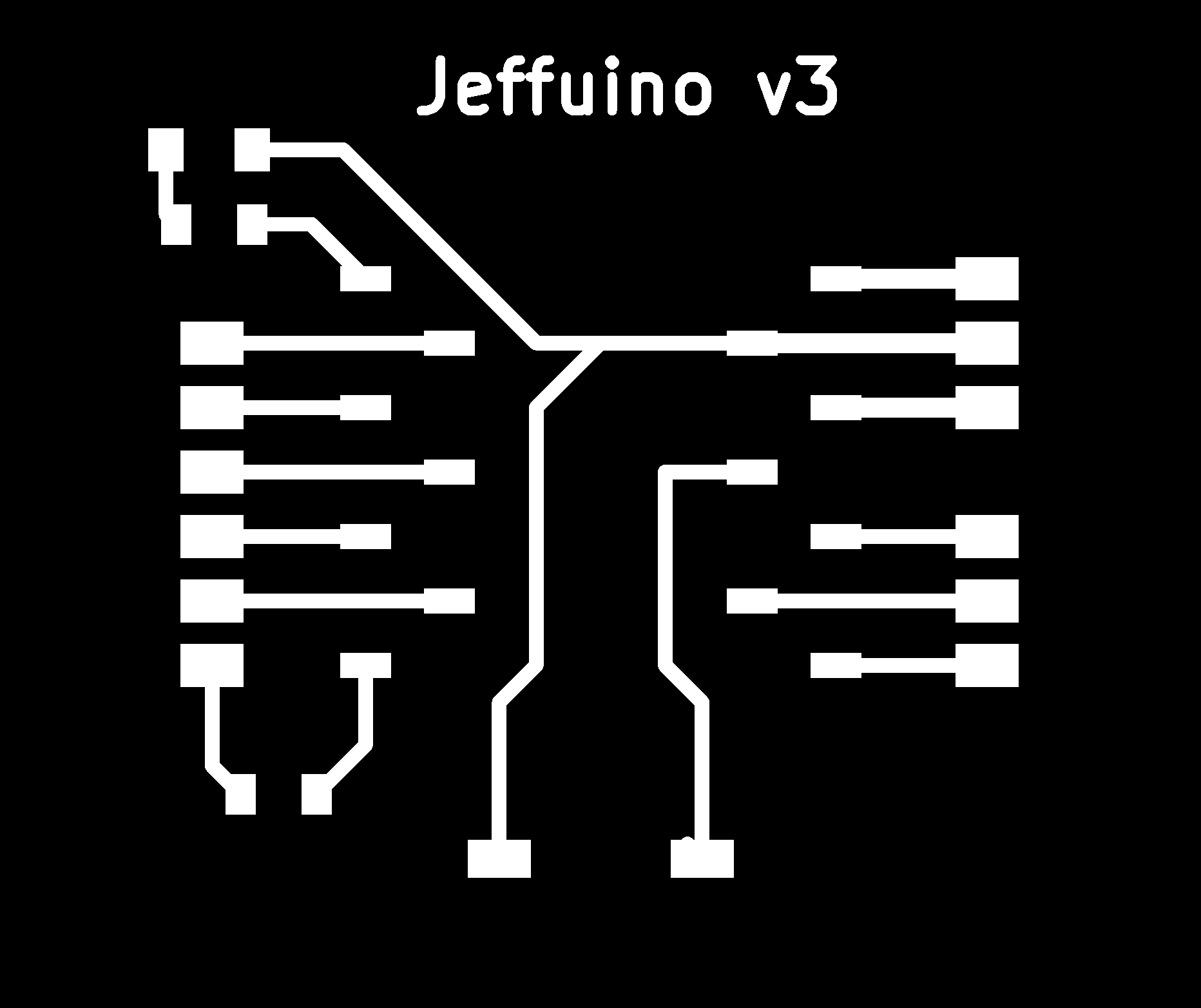
Each board requires a capacitor across voltage and ground and the tutorial on Adafruit recommends a resistor on the first digital in of a neopixel string. That being said, because the resistor only needs to be in series with the first neopixel- it would be pretty wasteful to add resistors to every board AND would add up (80 330ohm resistors would create a lot of problems for the circuit by adding that much unneeded resistance). I decided to redesign the jeffuino (now v3) to include a 330 ohm resistor on the d6 pin. This would keep the pcbs modular and allow me to add the resistor easily.
Going forward, I will need to think about how to run the data and the 5V power across all 80 some LED boards. The current setup doesn't really allow for running data in a "net" nor does it allow for adding multiple instances of five volt power to the neopixels throughout the net of LEDs.
When I tested the stray neopixel on the new Jeffuino v3, the neopixel didn't work. As I had mentioned earlier, in testing I discovered that the 330 ohm resistor interefered with the digital in signal.
Batch fabrication workflow
If I am to make 80 of these boards, I will need to automate the fabrication process as much as possible.
Gerber2PNG has a multi-layout function. Thanks Superfablab Kerala.
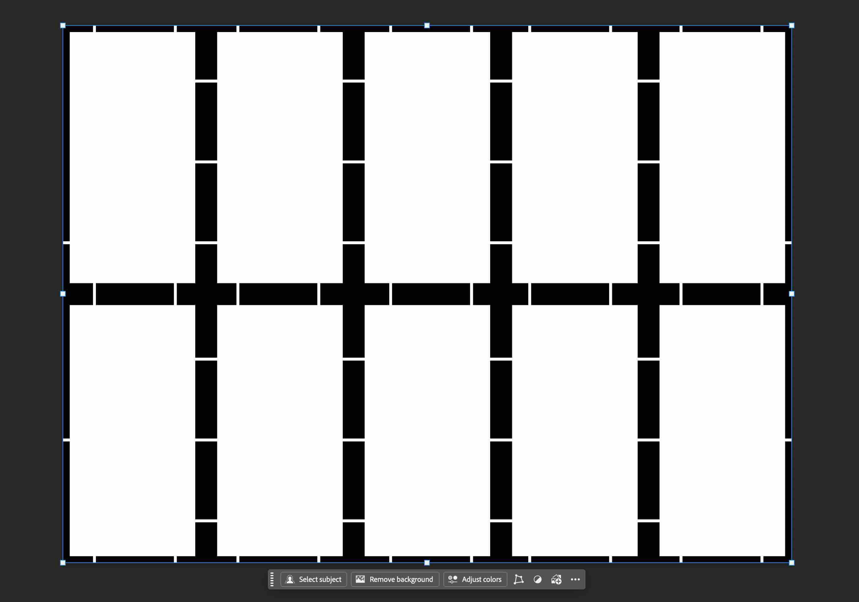
I upladed the gerber of my circuit, created a row of the pcbs.
My copper forms are 6in x 6 in, which means 152.4 mm. I had initially made a mistake in calculating the number I could fit. I downloaded the PNGs.
I first cut traces, then edges
Edges will pose a problem as I want them in a board to paste and reflow all at once. To solve this problem, I need to keep the boards in a group. To that end, I opened the edges png in illustrator and added white lines to serve as tabs in the agrouped pcbs. Doing so would allow me to create a template, paste and solder all of the grouped pcbs at the same time. Doing so would help me be more productive.
Milling issues
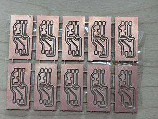
I started to cut the grouped boards. I used a vbit to cut the traces and then a 1/32 squre end bit to cut the edges. I ran into two problems. The first was commented on by previous students- if your computer falls asleep while running your mill from mods via usb, the mill will stop cutting. This happened to me. The second problem is with the outlines, as the board came loose from the sacrificial layer. I also noticed that the width of the space between the boards caused the SRM-20 to have to mill much more than just cutting lines.
As I was cutting the edges, the board broke away from the sacrificial layer after about half way through the cut. I retaped and reapplied it to the sacrificial layer, and then attempted to line up the zeroed axes with the board so that I didn't lose the boards I had made and waste the copper forms. Largely eyeballed the mill bit as I lowered to the newly fxied board, attempting to line up the spindle/mill bit with the previous board point of origin. I was pretty close.
I cut the previous trace program and it worked really well.
The tabs were pretty effective and the boards came out as a group. I would likely add more tabs to ensure that the boards don'tbreak apart
If I could ask one thing of the good people in Super Fablab Karela, it would be to add a tab function to the gerber2png page.
Paste template fabrication
I figured out how to make a template mask for solderpaste. Under file>plot> the following interface comes up. From the plot format drop down, select SVG and then the paste layer
In pcb viewer, I opened the PCB that is ready to be cut and selected file>plot. In the plot UI, I selected format: SVG from the drop down menu. I then selected just the layer the edges are on (Edge.Cuts) and the F.Paste layer (which will serve as the top stencil). The Edge cuts will help in orienting the stencil. I pressed Plot to generate the SVG of the paste layer.
I edited the svg to delete any elements beyond the pads. I used inkscape to remove the fill of the pads, set the width of the stroke to 0.423 pixel and the color of the stroke to red or black- depending on what your laser cutter is set up for. The boxes should be slightly smaller than the dimensions of the pads to account for kerf and when fabricating, to prevent bridging.
The thickness of the material matters, as that will determine the amount of paste that you can put on the board. Thinner traces will require thinner paste templates- thicker traces may well require thicker template materials. According to Lady Ada, the rule of thumb is approximately 2.64 + 0.0831 * pitch-of-component then averaged.
Another paste template method
I also found that for the pads / paste template, I could use the gerber2png site to create a png- but I need a vector to laser cut. You can import the png into Inkscape, used the path>trace bitmap command to create a file that I could export as an SVG.
I had forgotten to bring the sheet of Kapton / polyimide (2 mil or 0.0508mm thick), but decided to do a test run of the paste pad template using a piece of 0.8mm thick piece of cardboard (the backing of graph paper). Epilog edge laser cutter. Speed 25 power 30 and freq 500. The template came out perfect, albeit perhaps too thick.
I came in again with the kaptone sheet. To laser cut the kaptone sheet, I used the following settings on vector cut using the epilog 40 w laser.
Speed 100
Power 10
Freqeuency 100
I ran out of time to get the reflow machine set up and working, but I have made progress toward understanding this output device and have a better concept of the LED components/pcbs I will need to fabricate for my final project.
DFPlayer Mini MP3 player
Because I want to include sound in my final project, I worked with the DFROBOT DFR0299 DFPlayer Mini MP3 player.
I followed the online manual and a linked tutorial, below:
DFPlayer Mini MP3 Module for Arduino and ESP32 Projects | DFRobot Wiki. “DFPlayer Mini MP3 Module: Elevate Your Arduino and ESP32 Sound Projects.” Accessed March 28, 2026. https://wiki.dfrobot.com/dfr0299/.
DFPlayer Mini Reference: API, Protocol and Pinout | DFRobot Wiki. “DFPlayer Mini MP3 Player - Unlock Full Potential with Specs ?” Accessed March 28, 2026. https://wiki.dfrobot.com/dfr0299/docs/20905.
I first breadboarded out the board to prototype. This requires four buttons which are used for control. The mp3 player requires 5 volts.
I first installed the libraries and then I uploaded the following sketch, which operates the mini mp3 player and uses the buttons to play, stop, increase/decrease volume, and go to next/previous song:
RX and TC from board- D7 and D6 on the jeffuino. The corresponding pins on the Xiao are the UART pins on the RP2040.
"UART or Universal Asynchronous Receiver-Transmitter (UART), is "a serial communication protocol that can be used to send data between an Arduino board and other devices. This is the protocol used when you send data from an Arduino to your computer, using the classic Serial.print() method.
UART is one of the most used device-to-device (serial) communication protocols. It’s the protocol used by Arduino boards to communicate with the computer. It allows an asynchronous serial communication in which the data format and transmission speed are configurable. It's among the earliest serial protocols and even though it has in many places been replaced by SPI and I2C it's still widely used for lower-speed and lower-throughput applications because it is very simple, low-cost and easy to implement.
Communication via UART is enabled by the Serial class, which has a number of methods available, including reading and writing data."
I loaded three mp3s on the sd card, inserted the card, and then connected the mp3 player to the Jeffiuno using 5v, ground, rx and tx lines. The board can only power speakers up to 3 watts, and I have a bunch of old speakers I've pulled from broken toys and devices. I used a .5 watt speaker.
I uploaded the sketch to the jeffuino and nothing happened.
I referred to the manual, which suggested that if the board doesn't play music, try to the volume button
I turned up the volume. Success.
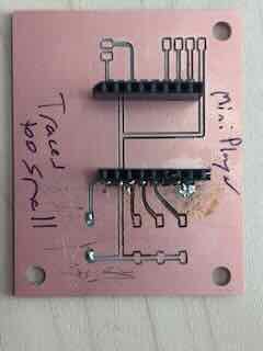
I only have access to two of these boards and they came with pins pre-soldered in. As I had done in electronics production, I will use female connectors to create a PCB that will allow me to remove the DF Player mini board.
The miniplayer is not in the kicad pcmfab library, so I will use two eight pin female connectors and mount them on the pcb I create. The pitch is 2.54, which will accommodate both the board and the footprint for the SMD connecter footprint in the PCMFAB kicad library.
I created the board, added four buttons and two sets of horizontal pin headers. I had made the board larger initially so that I could hot glue the speaker to the board if I was going to mount it. I added three mounting screws to the board, just in case I need to mount the board on the final project. I followed the process for fabricating a board and developed the following traces file:
I had some trouble getting the traces the right size, which I think is a result of the fabrication process I was using.
I completed the board.
I connected the new board to the Jeffuino as I had before, plugged in the Jeffuino, and we are in busines.
.png)
.png)