Week 08 Electronics Production
This week we were charged with:
group assignment:
- characterize the design rules for your in-house PCB production process
- submit a PCB design to a board house
Individual assignment:
- make and test an embedded microcontroller system that you designed
- extra credit: make it with another process
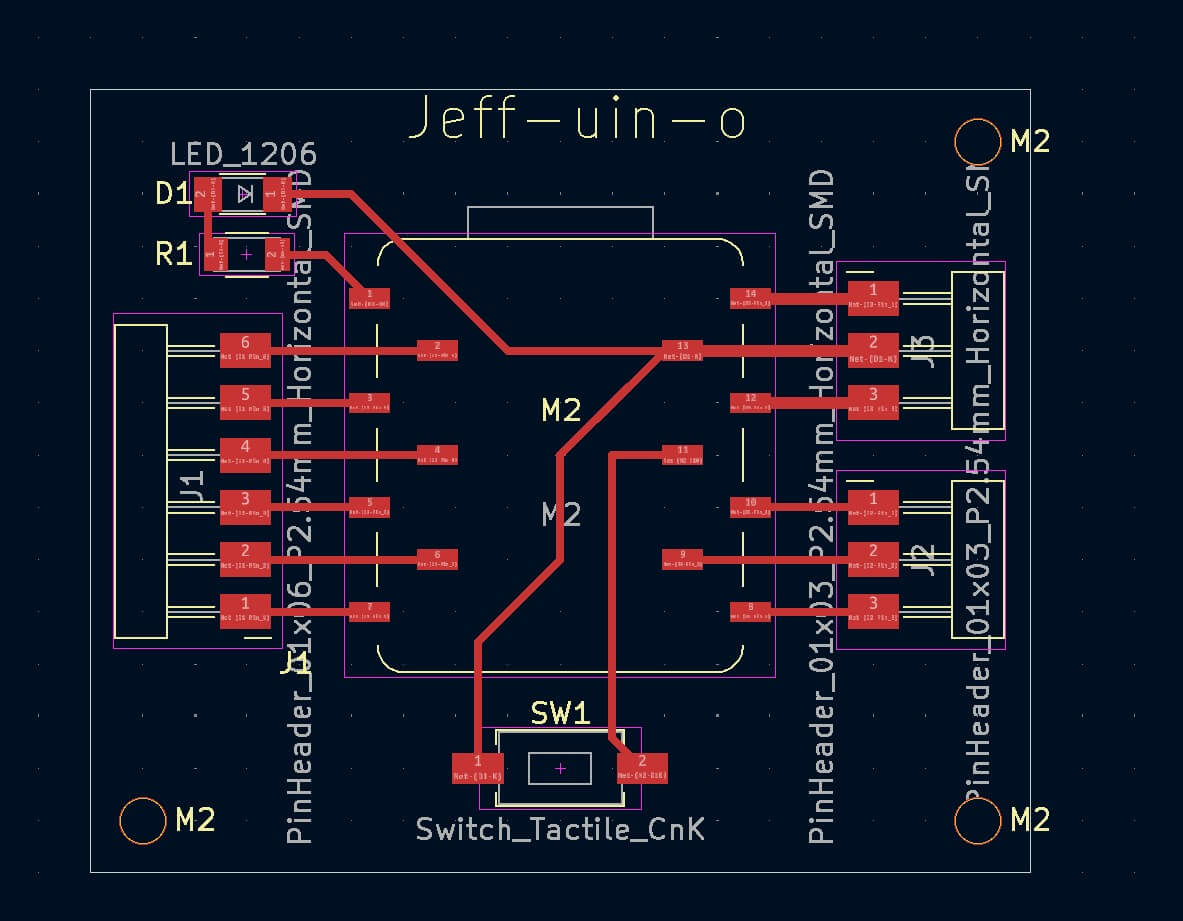
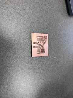
The Jeff-Uin-O
Before I decided to try cutting my board, I posted a photo of board to mattermost.
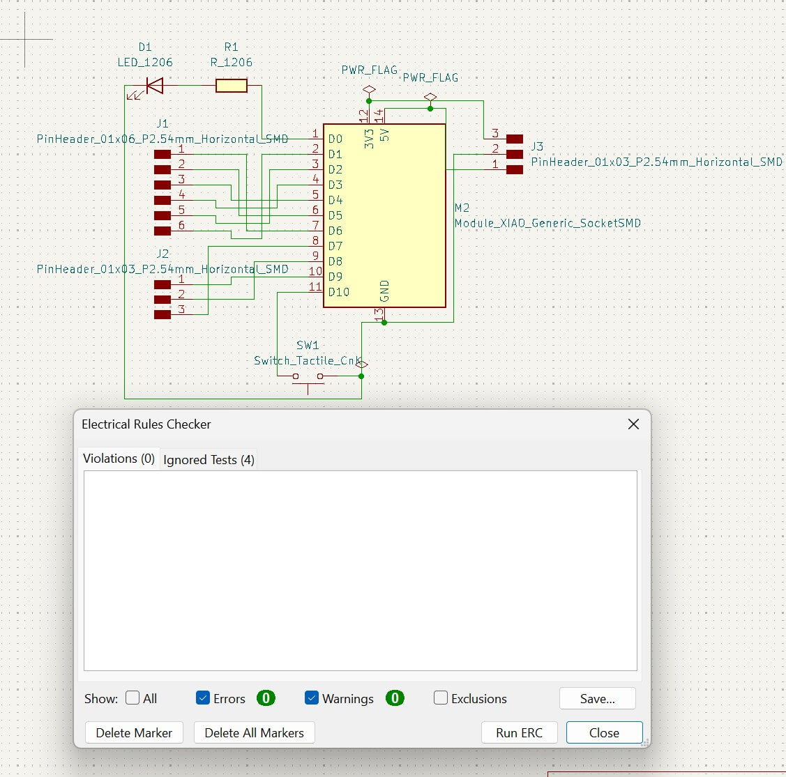
Received feedback on it. Based on this feedback , I revised the board. I found that by straightening the components the traces better align. I call my board the Jeff-uin-o (djeff-WEEN- oh). The schematic passed the ERC.
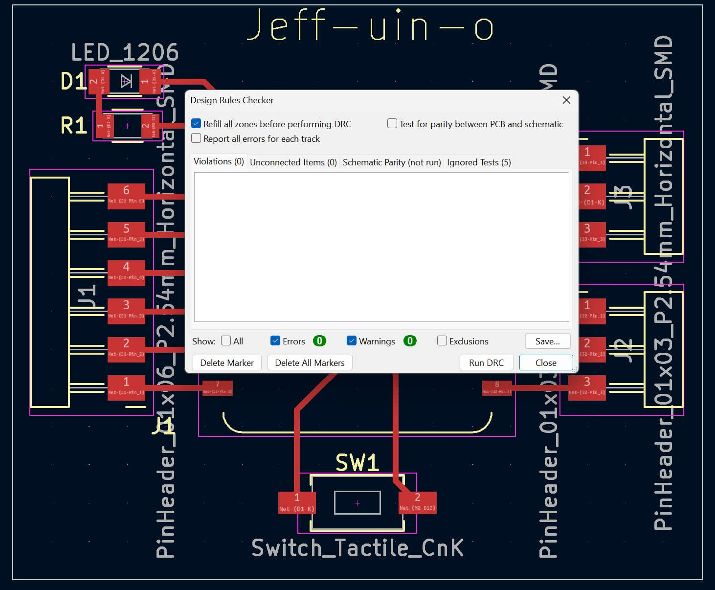
The board took a little while to layout, but I was happy with the result. I added mounting holes and was good to go.
Submit a PCB design to a board house
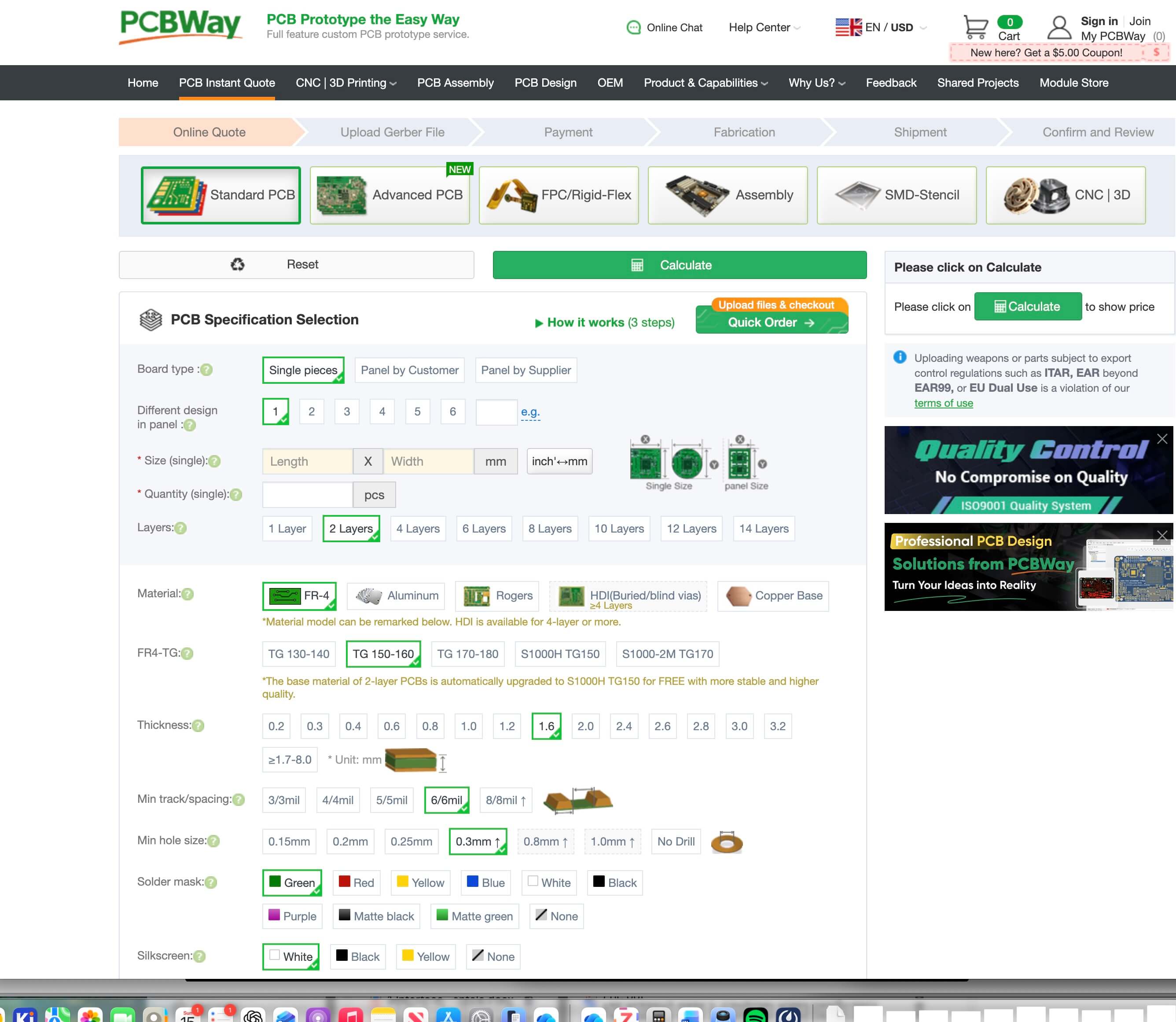
I decided to use https://www.pcbway.com/orderonline.aspx
Submitted
The initial response was that it would cost $6.5 to create 5 boards with a 24 hour turn around. There were 2 Layers Size 38.1x45.72mm 1.6mm\
pCBwayreview failed
I submitted the pcb to the board house, but the pcb failed. The reason stated was:
All the layers are repeated.;
There is no drill layer in the file. If you do not need drills, please contact your service rep to change the parameter as "No drill".;
Lack of the Soldermask layer.;
I didn’t know what this means and so entered the file and message and URL into chatgpt.
Prompt
What does the following message mean from a failed pcb review on https://member.pcbway.com/order/cartlist
Failed reason:
All the layers are repeated.;
There is no drill layer in the file. If you do not need drills, please contact your service rep to change the parameter as "No drill".;
Lack of the Soldermask layer.;
I can submit a zipped gerber file if you can read it.
I submitted the contents of the gerber file directory in my kicad project director, not the zipped file in the production directory. I submitted this directory.
Failed again
The reason the site gave:
Please confirm if it is a 1-layer or 2-layer board.;
There is no drill layer in the file. If you do not need drills, please contact your service rep to change the parameter as "No drill".;
Given how long it took to get this far, I decided to proceed with my board as is.
Fabricating the PCB
Before I started fabricating, I refered to the following tutorials:
“PCBs with Roland MDX-20 | Fab Academy Tutorials.” Accessed March 12, 2026. https://pub.fabcloud.io/tutorials/electronic_production/mdx20/.
“5. Electronics Production - Fab Academy Quentin Bolsee.” Accessed February 27, 2026. https://fabacademy.org/2020/labs/ulb/students/quentin-bolsee/assignments/week05/.
“Double Sided PCB Made Easier!” Accessed March 12, 2026. https://sibusaman.fabcloud.io/doublepcb/.
“HTM(A)A with Zach.” Accessed March 12, 2026. https://fab.cba.mit.edu/classes/863.19/CBA/people/zach/week03.html.
“Instructor Bootcamp 2024 - Instructor’s Bootcamp 2024 - Fab Academy.” Accessed March 12, 2026. https://academany.fabcloud.io/fabacademy/2024/bootcamp-instructors/workshops/Soldermask/.
“Kai Zhang’s HTMAA.” Accessed March 12, 2026. https://fab.cba.mit.edu/classes/863.23/Harvard/people/Kai/index.html#week_6.
“Week 08, Electronics Production - Charlotte Super Fab Lab - Fab Academy 2025.” Accessed March 13, 2026. https://fabacademy.org/2025/labs/unccharlotte/assignments/week08/week08/.
Milling
For this assignment, I am milling- in which the cutter is turning and the part is held stationary. I am basing my definitions/explanations of the milling process on content from John Hart’s MITx 2.008x Fundamentals of Manufacturing class and the Kalpakjian and Schmid Manufacturing Engineering Technology book.
Machining is good on flat and curved surfaces and can achieve tolerances of up to 0.001 inch.
Rotational Speed (N ) is the speed of the milling cutter/spindle spinning, measured in RPMs.
Cutting speed, surface speed, and tangential speed (V or Vc) are essentially equivalent and refer to the speed of the tool and the surface of the workpiece being cut. It is measure in distance over time (e.g. mm/seconds).
There are a lot of terms that use the term Feed. Feed is different from feed per tooth and is different from feed rate.
In milling, Feed (f) refers to the width of material removed per revolution of the tool, measured in [distance]/[rev] (such as [mm]/[rev]).
Feed per tooth an end mill (or similar tool) can have a number of teeth (e.g. 2 or 4). Each tooth/cutting edge is essentially an independent tool To standardize calculation, the feed per tooth (ftooth) is used, which is the feed divided by the number of teeth of a cutting tool.
Feed rate /linear speed (v) the speed at which the tool axis moves relative to the workpiece iself. Measured in distance/time. Feed rate is always less than cutting speed.
To increase the area of the cut- by changing the feed or depth of cut, increases the cutting force.
Climb milling the tool enters the workpiece at the surface of material to be removed
Conventional milling- the tool enters the workpiece at the cut surface worse surface than climb cut
Characterize the design rules for your in-house PCB production process
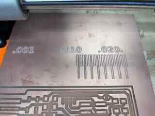
For the milling of the board, I have available 6 in x 6 in Circuit board blanks (2-sided FR1) and a Roland Monofab SRM-20
I used the gerber to png app at https://gerber2png.fablabkerala.in/
Generated gerber files using kicad command under file
I should place the material on the sacrificial layer. Usually you would use double sided tape, placing the tape first on the material and then removing the backing and placing it on the sacrificial board. The material had already been placed on the board, so I didn’t need to do this this time around.
I then changed the milling bit to a 1/64 se end mill
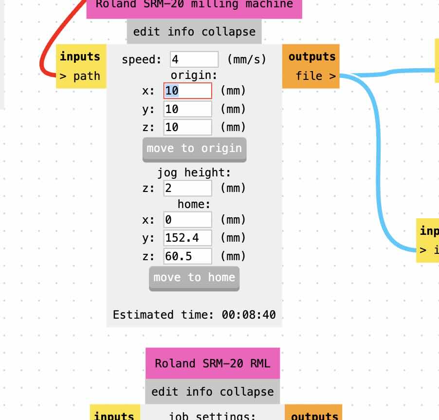
I opened the V-panel software, which is used to control the SRM-20.
I zeroed the x and y axes by moving the bit to approximately the x and y coordinates that I wanted to set as the origin. The Vpanel control panel has four settings for movement, continuous, 100, 10 and 1. I would use continuous for gross moves, and then to fine tune would use a decreasingly smaller increment of movement. Press the zero xy button to zero.
I zeroed the z axis by moving the z to approximately a little above the height of the board. ,
I slid a piece of paper under the bit and lowered the bit using the 1 down z button until the paper didn’t move. I then pulled the paper out and I pressed the z axis zeroing button. The z axis is zeroed. (NOTE- even though I'd read the other documentation, I did this, which was a mistake based on how you would zero the z on an old 3d printer. I am a knothead).
I imported the test traces file into imodela creator (NOTE- imodela was another problem)
1/64 is 0.015625 inches. I set the width to 0.016 in the software
The measurement for the board was 6 x 6 x 0.07 in.
Because I had previsouly made a test cut on the material- removed 2 inches, which means that the board is approximately 4 x 6 inches.
I set the depth of cut to 0.004 in
Type of cut -- engraving
I ran the program.
Nothing was cut.The mill moved above the board, but nothing cut.
I re-zeroed the z by moving the z down until the bit almost touches- and then loosening the bit so that the bit drops to touch the material and retightening.
I used the defaults for engrave, and pressed the cut button.
The cut took over an hour. It was super slow. It was too large. I eventually had to stop the cut.
I went to GOT and was advised to use mods rather than IModela.
I pulled up mods and selected Roland SRM-20 2d pcb. I imported the PNG of the traces
I chose engrave 1/64th, connected the mill to my computer by usb, and sent the file to the mill.
It moved 10 mm over the surface of the board. I had read this…and was told this in GOT- but forget to change that setting. I changed the offsets in mods and ran the program again- the cut was quick, but the bit didn’t remove enough copper to create traces. I believe that the z was too high.
Because I had cut a pieces from the board previously, I measured the remainder of the board through using the x and y movement on Vpanel.
I then used mods to cut my board
It might be easier/more effective to run mods off of the desktop, but when I tried, for some reason mods would not send the file to the mill. I decided on running the mill using mods on my laptop. For some reasons, the pause,home buttons either didn’t work on mods. The Vpanel software was on a desktop, so I had to pull the usb out of my laptop, place it in the desktop and then press pause or zero. I will explore this further.
I used the feed, speed, and depth of cut from the mods program.
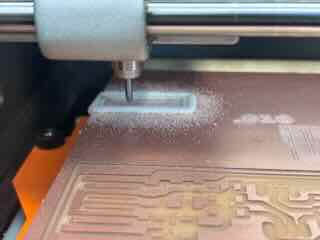
While engraving the traces, the 1/64th mill bit broke. I installed a second, reset the z and cut the traces again. The engraving worked.
I uploaded the outline, changed the mill bit to 1/32, recalibrated the z, and then used mods to cut the outline of the board.
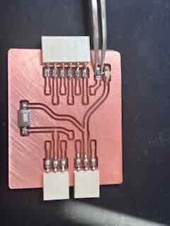
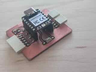
Completed board
The piece seemed well-executed. I followed the same process to print two more as spares in case I ran into problems
The second board broke the second 1/64th in bit. Clearly something was wrong.
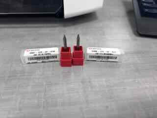
Both of the 1/64 bits broke, so I used the 1/32 FE bit end mill to cut the traces. The last board was cut well.
Lesson learned
My z might have been too high, and the bit too far out, which would explain the broken bits. I just plugged this question into chatgpt and according to chatgpt my bits were too far out of the collet. My bits stuck out of the collet by over an inch/ 20 mm—or more, creating a lever out of the bit that would make it more likely to break the end.https://chatgpt.com/share/69b80455-e48c-800f-83bb-ceb6aac1a4e7
Folks in the class verified that this was the case. The more the milling bit sticks out of the collet, the more the bit acts like a lever arm. You need to keep a relatively small amount of the bit outside of the collet- like under 10mm.
"Assembly and testing workflow"
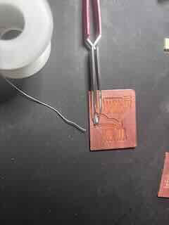
I washed the three boards.
I then sanded the edges and faces of the boards to remove the burs on the edge and to allow the solder to better adhere to the copper.
To assemble the boards I used a Hakko soldering iron with the smallest soldering iron tip we had available.
I have to order an additional part that was not in my lab's inventory, so I am waiting for the parts to arrive.I first soldered a button.
I had an old flexible circuit that I thought would be fun to dissasemble and recycle the smd LEDs from that circuit- and it provided a good opportunity to practice my multimeter skills. The LEDs were 1206 sized.
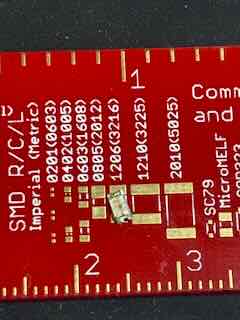
I used the multimeter to determine the forward voltage of the LEDs. I was unsure of which was annode and which was the cathode. The LEDs have a green mark on them-- I tested contuinity using the mm and it was clear that the ground was on the green side. Green is ground. Easy to remember.
I changed the MM to the diode test and determined the forward voltage drop was approximately 2.2V.
Based on this voltage drop and the 3.3 v power provided by the gpio pins on the XIAORP2040, I determined that a 330ohm resistor would work in this instance. I added that to the board.
I wanted to check to see if the components worked and if there were any problems with the soldered joints. I used a multimeter to test the button (I placed the MM on either side, set to continuity, and pressed the button. The MM didn't sound until i pressed the button.) I tested the led by running 4.5 volts through the circuit traces I'd cut. The led lit up.
I then added the horizontal connectors. I realize that we are supposed to start from the large and center and work our way out, but I was waiting on the parts I had ordered and didn't want to wait any longer to solder the boards. If something happened, I had two spares.
I used the multimeter to test the continuity of the board and its components. No shorts, everything appears to be working.
I had to wait to receive the parts to insert the xiaorp2040 into the board, but when they arrived I realized (too late) that these elements have a pitch (distance between the holes) and that I had purchased the wrong one.
Damn it.
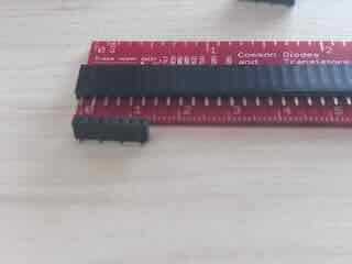
I really don't want to wait an additional week to receive the correct parts. I had a number of through hole female connectors.
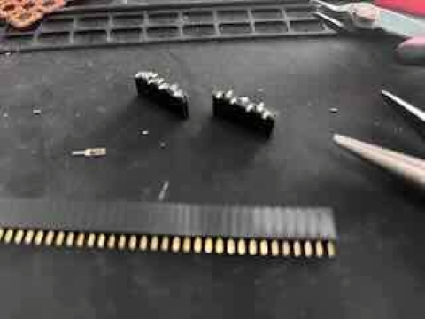
I used a pair of cutters to trim the header to seven holes/pins, and then used pliers to bend the through hole leads to alternate (and match my board). I super glued the leads to the bottom of the component so that the parts would not short and to keep the leads in the board and soldered my makeshift vertical connector onto my board.
I had a few problems with soldering the connectors to the board (a bridge I had to repair), but I finished.
I loaded this blink program to the board and the LED functioned as expected.
I then loaded this revised sketch to the board and the light lit up when the button was pressed. It worked.
Files
Blink sketchbutton/blink sketch