Week 06 Electronics Design
This week we were charged with:
group assignment:
- use the test equipment in your lab to observe the operation of an embedded microcontroller
individual assignment:
- simulate a circuit
- use an EDA tool to design an embedded microcontroller system using parts from the , and check its design rules for fabrication
- extra credit: try another design workflow extra credit: design a case
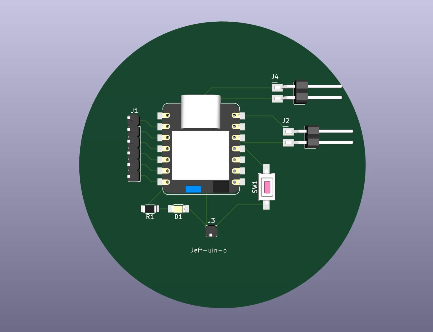
My board for this week....the Jeff-uin-o (Dhef- WEEN - oh)
Electronics Overview
I started out with an overview of basic electronics and circuits. I’ll use my notes and Forrest M Mims III, Getting Started in Electronics, Master Publishing, 2000 to explain terms.
Voltage (V)
volts (V) electric potential difference (Note- just as you can’t measure height by just measuring someone’s head, you have to measure in two points, voltage is measured between supply voltage and the point where the voltage is zero, or ground)
Current (I)
ampere(I) flow of electrical charge past a specific point in circuit
Resistance (R)
Ohm (Ω) opposes or impedes the flow of current
Power (P)
Watt(W) energy per unit of time
To build a circuit, you need to make sure the power supply/battery is capable of supplying the power the circuit needs. Additionally, electrical components have maximum voltage/current ratings that should not be exceeded.
Ohm’s law V=IR
V/IR
Voltage(V) = current (I) * resistance (Ω)
Current (I)= voltage (V)/resistance (Ω)
Resistance (Ω) = Voltage (V)/current (I)
Kirchhoff’s current law:the sum of currents entering a node must equal the sum of currents exiting the node- or the sum of currents entering and exiting a node equals zero. This law is like a rule for how water flows at a junction (where pipes meet). It says that the total amount of water (or electricity) coming into the junction must equal the total amount of water (or electricity) going out. This makes sure that there's no water (or electricity) magically appearing or disappearing
Kirschoff’s voltage law the sum of voltages around any closed loop in a circuit must equal zero. Batteries "add" voltage and resistors experience a "voltage drop." This law is like a rule for the energy of the water (or electricity) in a closed loop of pipes. Imagine you have a water pump that pushes water up a hill, and then the water flows back down the hill. The energy gained by the water going up the hill must equal the energy lost when it goes back down. KVL says the same thing for electricity: the total voltage (energy) gained in a loop must equal the total voltage (energy) lost.
voltage drop when electricity flows through each part of a circuit, it loses some energy, i.e. voltage drop. Voltage drop is that amount of energy lost as electricity moves through each part of a circuit. The more resistance there is in each part of the circuit, the greater the voltage drop for that part.
Ground point defined as zero volts. The term "ground" refers to signal common. Battery-ground is implied as the negative terminal of the battery-but that doesn’t mean there is ground NOTE, if using two voltage supplies in a circuit, you would want to create a common ground
Schematic Convention- place power sources in schematics at the top, i.e. with current flowing down
Testing
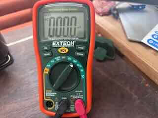
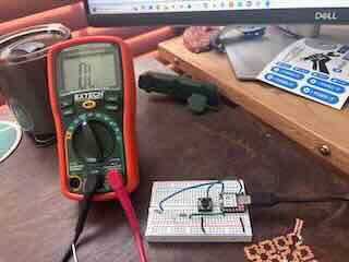
For the group assignment, I will work on it on my own and be using the Extech EX330 autoranging multimeter MM, which is a nice and fairly affordable multimeter. I have access to a Hantek2000 Series Handheld Oscilloscope 2D42, but I can’t get it to work.
Given that we will be building circuits later in this class, I can use the MM to measure voltage drop, resistance, and capacitance as well as continuity.
Measuring voltage/voltage drop
Change the rotary dial to select VDC
The voltage needs to be on the circuit when running. Place the red and black probes on either side of the wire/circuit or component.
Measuring current
Change the rotary dial on the MM to one of the As- 10A, mA or microA. I was taught that if you don't know the current running through the circuit, err on the side of being too large than risk buringing out the fuse. You need to place the probe cables appropriately in the device, but the MM shows which input is for which function
Measuring Continuity
Note- do not measure continuity while circuits or wires have voltage on them. Measuring for continuity is to determine whether a small element of a circuit, wiring/traces or the component itself- allows for the flow of voltage. It is helpful in that we can check to see whether the part/wiring is working.
On this MM, you have to use the mode button to switch between measuring resistance, diodes, capacitance, and continuity. Turn on the sound /continuity.
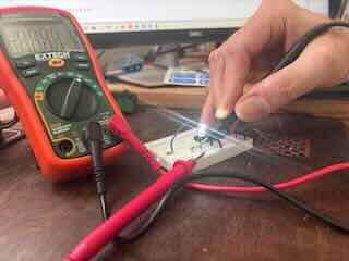
I had a flexible circuit printed on the vinyl cutter than I could not get to work. I set the MM to continuity, changed the mode, and could identify the traces that worked, the resistor I’d soldered functioned, but the soldered LED showed that there was no continuity.This is a really helpful functionality when checking circuits.
Video of me checking flexible circuit
Measuring Resistance
Set the MM to the ohm marker and use the probes to touch either side of the circuit or component being tested.
Logic Analyzer
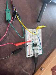
I do not have access to any fabricated fab boards and have not yet fabricated my own, so I will use a xiao rp2040 on a breadboard and will recreate the boards that way. I referred to Adrian’s documentation to understand how to use the logic analyzer.
“Week 06. Electronics Design.” Accessed March 1, 2026. https://fabacademy.org/2020/labs/leon/students/adrian-torres/week06.html.
I downloaded the Saleae software as he instructed
"Download Logic 2 - Saleae." Accessed March 1, 2026. https://saleae.com/downloads.
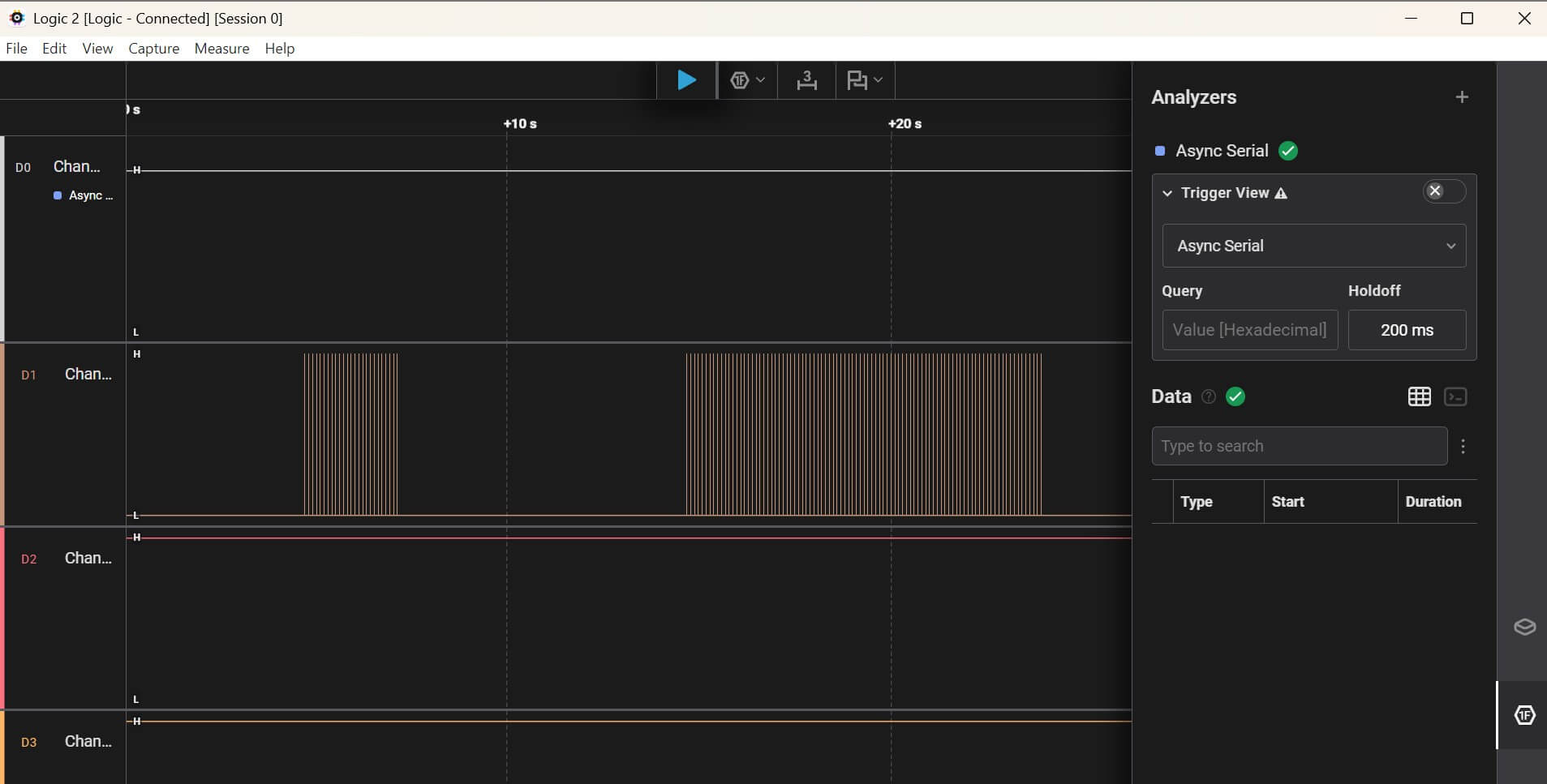
I followed his advice and opted to use the hooks. I went to the Device Settings tab and configured the Trigger mode. This means that the logic analyzer will record data until it finds a digital trigger. I selected channel 2 and set the capture for 1 second.
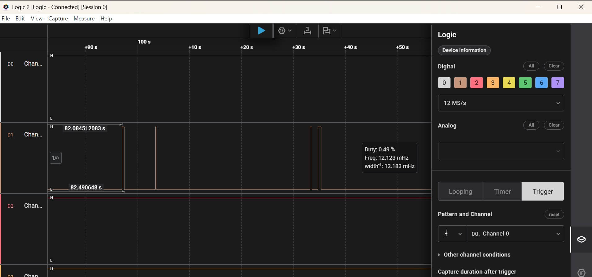
I pressed play and when I pressed the button, the signal was shown as long as I pressed it
Rolling the mouse wheel in or out shows you the record of the channel.
Because I am using an RP2040 XIAO, I used Neil’s hello.RP2040-XIAO.blink-echo.ino sketch
Neil Gershenfeld. "Academy.Cba.Mit.Edu/Classes/Output_devices/RGB/Hello.RP2040-XIAO.Blink-Echo.Ino." Accessed March 1, 2026. https://academy.cba.mit.edu/classes/output_devices/RGB/hello.RP2040-XIAO.blink-echo.ino.
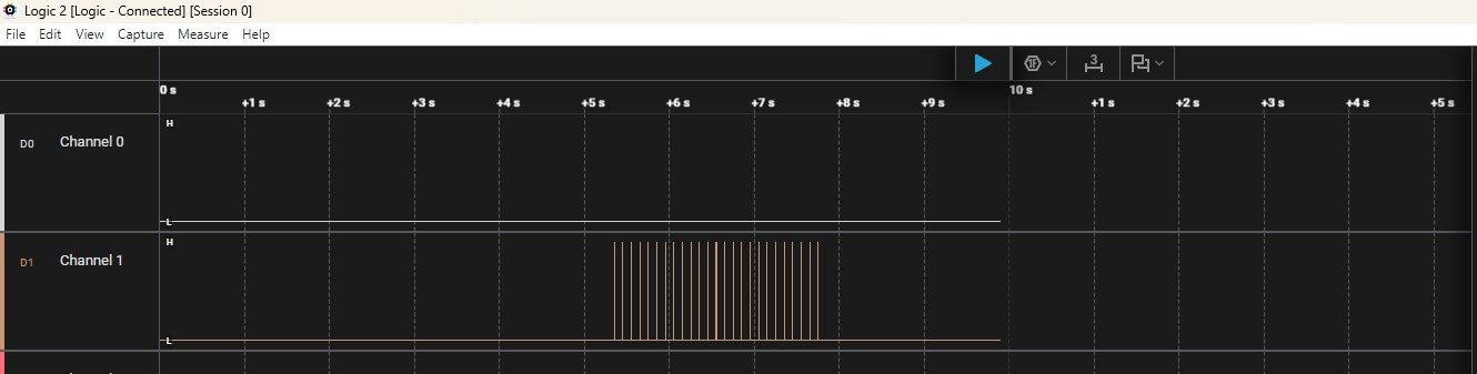
I changed the pins to reflect the pins I'd used in my sketch. I added a wire from the XIAO’s power to the voltage rail in the breadboard. I acknowledge that Neil doesn’t like breadboards. I had to change the baud rate to 115200. I pressed play on the software and then pressed the button on the circuit.
I deleted the settings from the first test
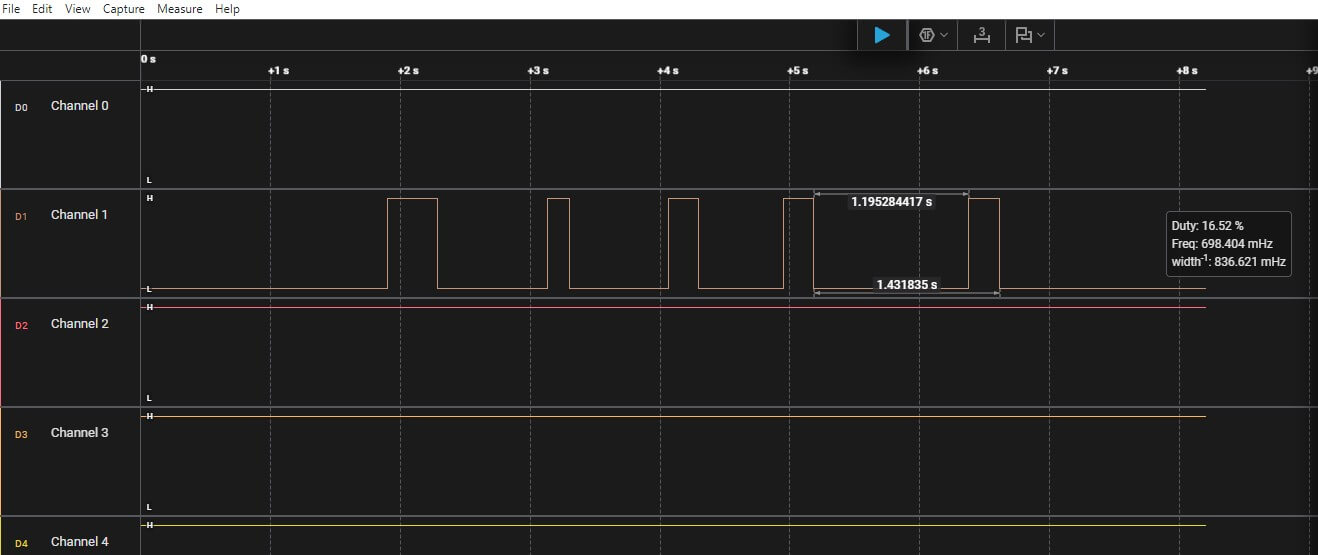
I changed the software so that it would recognize ASCII input. I set to trigger view, channel 1.I pressed play, and then I entered two phrases- hello and then this is a long message into the serial monitor. Success.
Simulate a Circuit
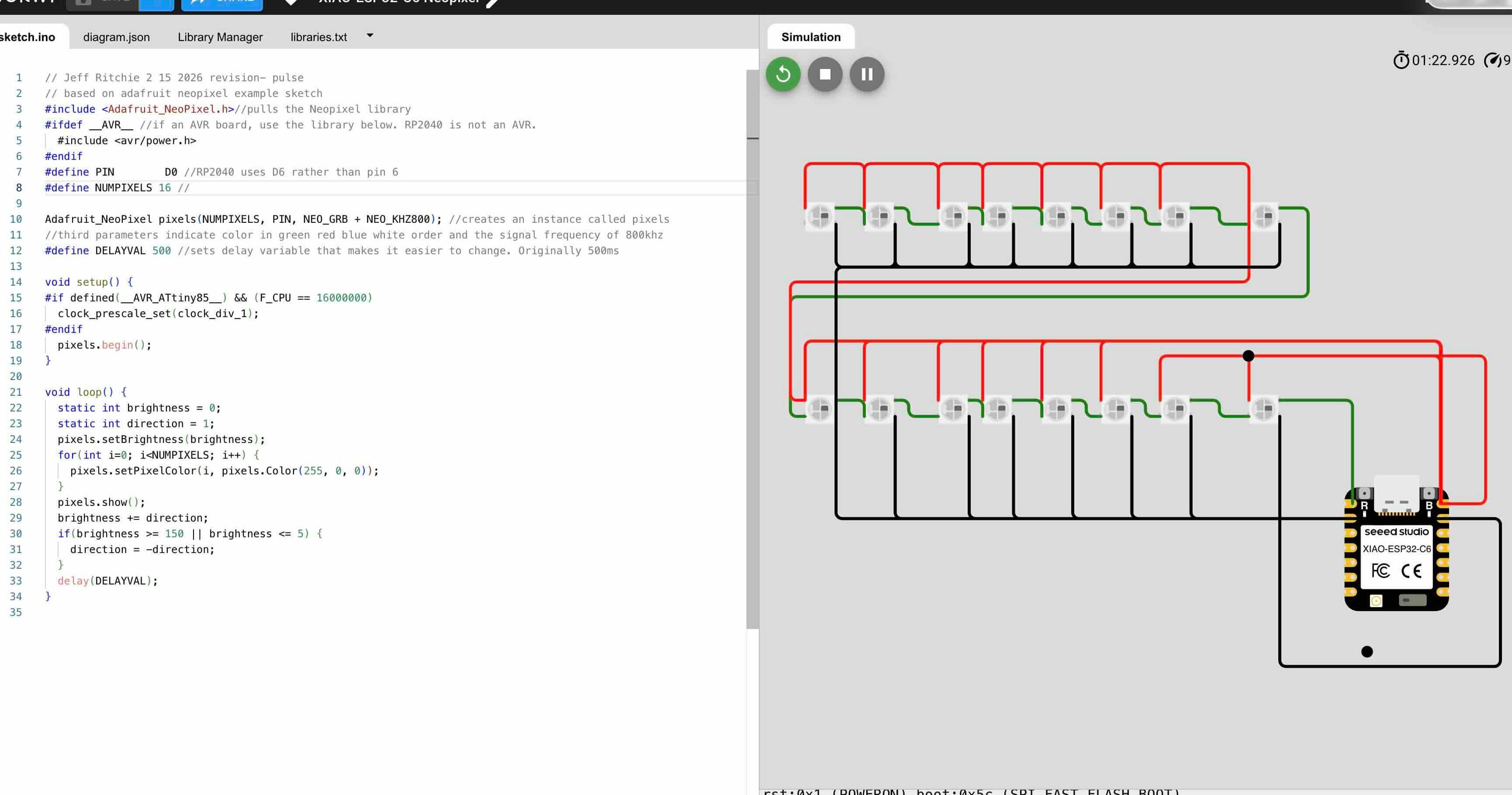
I started to use kicad to simulate a circuit, but ran into trouble setting it up. The existing tutorial didn't seem to cover simulation, so I switched to Wokwi for the purposes of this assignment. I wanted to simulate a circuit similar to what my final project would do by including neopixels. I could not access an RP2040 chip in the wokwi library, and the Pico only supplied 3.3 volts. I need a board that can supply at least 5V for the neopixels, so for the purpose of this assignment I used the XIAO-ESP32-C6. I know that I will need to power the NEOPIXELs using an external power supply rather than through the vout of the RP2040. I used the sketch I'd written for the embedded programming week. The neopixel in the simulation is not very bright, but did flash as expected. As an experiment, I had tried running the vdd and vss from the board to each neopixel and daisychaining the data through a series of neopixels. Both appeared to work in the simulation. Good to know. For my final project, I will daisy chain power, ground and data.
The link to the sketch is: https://wokwi.com/projects/457408666709350401
Designing a schematic and board
For this week our task is to design an embedded microcontroller system and check its design rules for fabrication. Based on the results of my simulation, I had intended to design a simple board that affords a "daisy-chainable" neopixel circuit that would easily connect with other neopixel circuit boards and provide the required capacitor between ground and power. The requirements of this week's assignment mean that instead I would need to build a microcontroller- not this LED board I had initially considered.
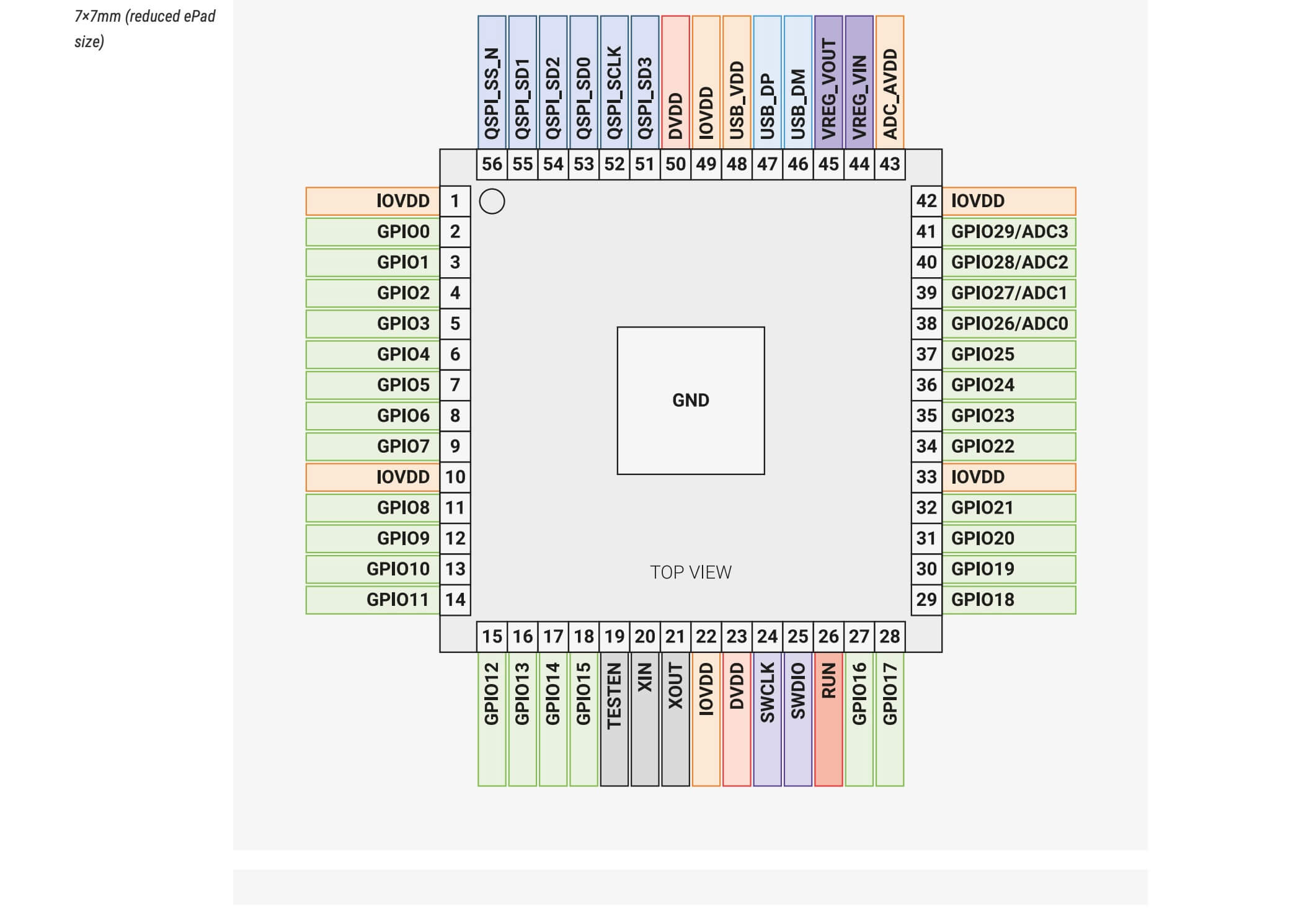
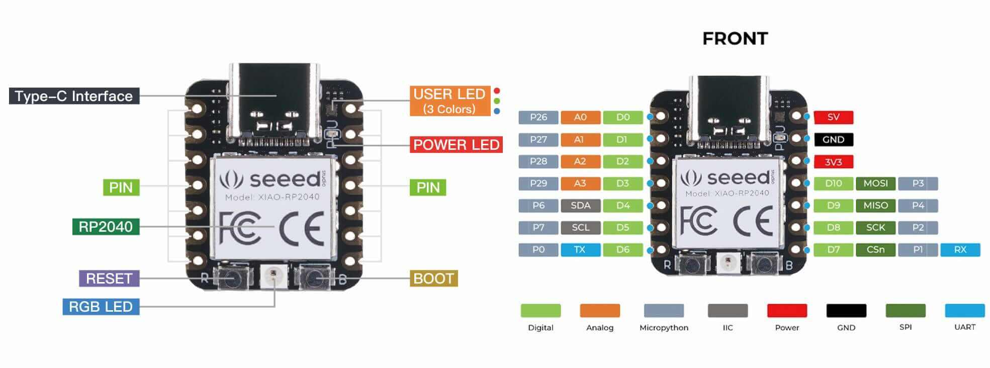
With that being the case, I initially tried to use the RP2040 chip. The RP2040 chip footprint in the fab library didn't look like the RP2040 footprint in the RP2040 datasheet. For the purposes of this assignment, I decided to use the XIAO RP2040 board.
| RP2040 Pinout | XIAO RP2040 Pinout |
 |
 |
My first step was to review the tutorial on how to use KiCad.
“Getting Started in KiCad | 9.0 | English | Documentation | KiCad.” Accessed March 1, 2026. https://docs.kicad.org/9.0/en/getting_started_in_kicad/getting_started_in_kicad.html.
Quoted from this tutorial, I made notes relevant to this week's assignment:
The typical KiCad workflow - two main tasks: drawing a schematic and laying out a circuit board.
The schematic is a symbolic representation of the circuit: Schematic symbols are pictorial representations of electronic components in a schematic. The schematic describes which components are in the design and how they are connected
the board is the physical realization of the schematic, with component footprints positioned on the board and copper tracks making the connections described in the schematic. Footprints are a set of copper pads that match the pins on a physical component. When the board is manufactured and assembled, the component will be soldered onto its corresponding footprint on the circuit board.
the board editor uses this information to make layout easier and to prevent mismatches between the schematic and PCB. The layout process requires careful placement of each footprint on the circuit board. After component placement, copper tracks are drawn between components based on the connections in the schematic as well as other electrical considerations, such as track resistance, controlled impedance requirements, crosstalk, etc.
Changes can be made in the schematic or board and pushed to the other design.
Helpful Keyboard shortcuts (copied/slightly amended from the tutorial)
Select objects by clicking on them while the selection tool is active- selection tool is active after quitting any active tool (Esc) or by clicking the button in the right toolbar.
Add additional objects to the selection with Shift+click - standard-
remove objects using Ctrl+Shift+click (macOS: Cmd+Shift+click).
You can toggle an item’s selection state with Ctrl+click (macOS: Cmd+click).
Drag selection -this is really helpful--dragging from left-to-right selects objects that are entirely enclosed by the selection box, while dragging right-to-left selects objects that are partially enclosed by the selection box. Shift, Ctrl+Shift (Cmd+Shift), and Ctrl (Cmd) can also be used with drag selection to add, subtract, or toggle from the selection, respectively.
Note - this was an issue for me when working on the circuit board- you can select an entire symbol (by clicking on the symbol shape itself) or select one text field in the symbol without selecting the rest of the symbol (by clicking the text). When just a text field is selected, any actions performed will act only on the selected text and not on the rest of the symbol.
Moving selected objects by pressing M and then selecting the objects
Rotate selected objects by pressing R and selecting the objects
Drag selected objects - use the G hotkey (drag) to move objects. For moving unconnected symbols, G and M behave the same, but for symbols with wires attached, G moves the symbol and keeps the wires attached, while M moves the symbol and leaves the wires behind.
Delete- Selected objects can be deleted with the Del key.
The Jeff-Uin-O
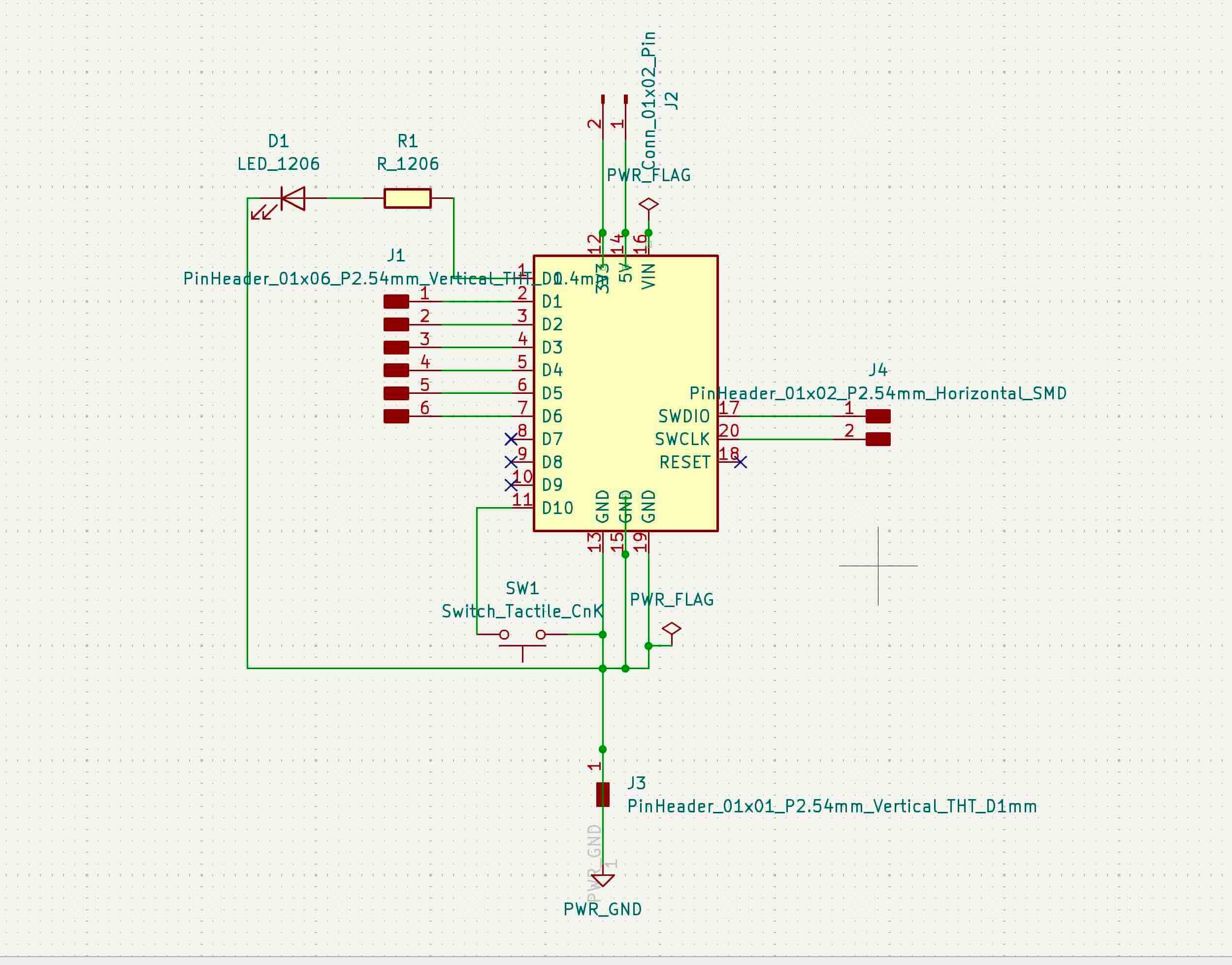
My goal was to create a pcb that will easily house and reuse the XIAO RP2040 board, as I only have one available to me and this microprocessor will be a lot easier to solder than the RP2040. I've added a standard mount for the board, as well as pins for power, GPIO and an LED and resistor for simple testing. The ultimate goal would be to use this board in my final project in order to control the Neopixels and take in data from the sensors.
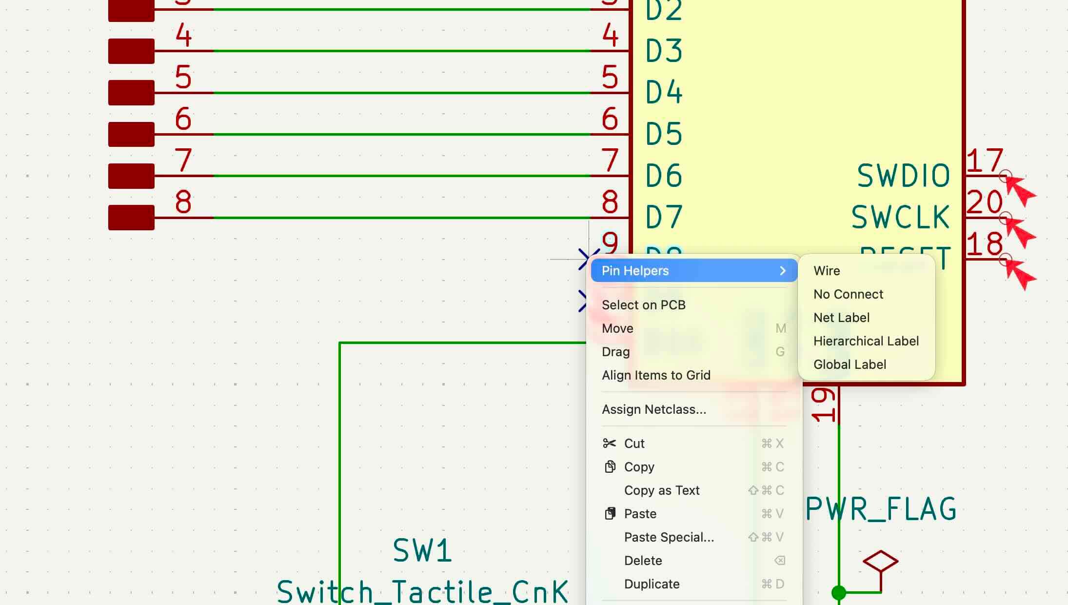
I added elements using the fab academy library as instructed for this week. I would search for an item, collapse all libraries, then choose the item in the fab library. The symbols have small circles on them that indicate where they are to be connected. I pressed W with the mouse over the circle and would draw the wires between symbol pins. Fairly easy.
The elements I added include:
I had initially added the XIAO RP2040 component to the board, but I was told by global instructors that if I only have one XIAO RP204, I should use vertical pins to allow the board to be inserted and removed from the pcb. I selected two female pin vertical headers to allow the XIAO to be mounted to the board. This allowed me to reuse my one XIAO RP2040 board I have at my remote location--and not permanently install it on one board.
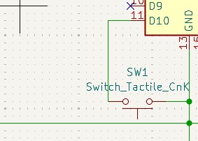
A button to allow for testing:
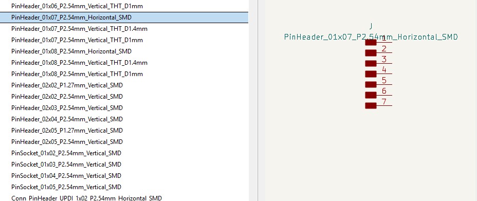
A GPIO connector to connect the board to other outputs or inputs:
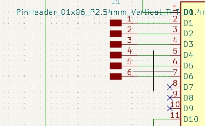
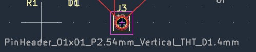
I added three pins 5v, 3.3 v, and ground to allow the board to power input and output components:
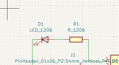
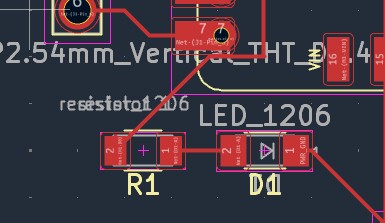
I also added an LED and resistor to allow for testing of the board
Finally, I added gpio pins to allow for I2C communication:
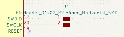
My schematic for the Jeff-uin-o is
Wiring the traces of the PCB

The PCB design for my Jeffuino board is:
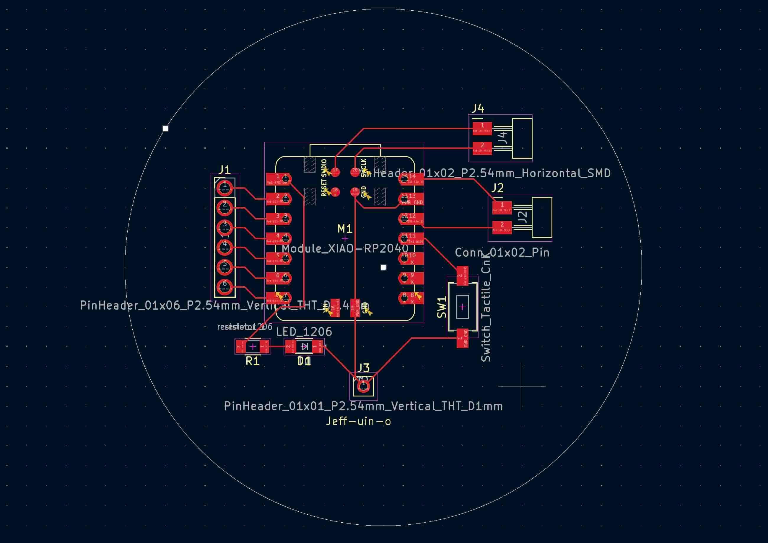
I opted for a round board in part to honor Neil's request for boards that are not square/rectangular.
I made a mistake in thinking that I could run ground to the back of the board through a throughhole connector. I had heard the idea during global open time and thought I would try it. It was not a good idea and I scrapped it after this board.
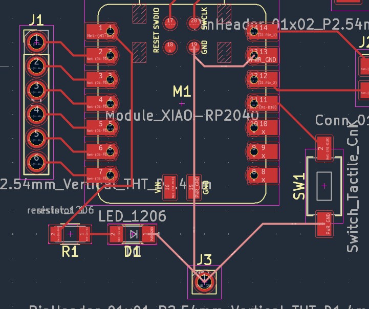
I thought it would be a good idea to place the LED and resistor at the bottom of the pcb- and run the trace from A0 down to it. It would make more sense to place the LED and resistor at the top of the board near A0.
Overall, I made a lot of mistakes in designing this board, which I came to understand when I redid this PCB during electronics production week.
The following are my notes on the overall process and key concepts/ideas in electronics design.
I clicked on the footprint Library browser tool to ensure that the footprints were properly assigned. According to the tutorial, the left pane of this window lists the available footprint libraries. The middle pane shows the symbols in the schematic. Some of these symbols have footprints and some need to have footprints assigned. The right pane shows the footprints that can be chosen for the symbol selected in the middle pane. To assign a footprint to a symbol, select the symbol in the middle pane and double click on the desired footprint in the right pane. You can preview a footprint by right-clicking the footprint’s name and selecting View selected footprint.
Ways to filter footprints
- The leftmost button activates filters that can be defined in each symbol. The tutorial states that it can be useful to turn this filter off in some situations.
- The middle button filters by pin count, so that only 8-pad footprints are shown for 8-pin symbols. This filter is almost always useful.=
- right button- Because we are to use the fab academy kicad library, its useful to use the right button which filters by selected library. Libraries are selected in the left pane; footprints not in the selected library will be filtered out. This filter is useful as long as it is known which library contains the right footprint. Often it’s best to use this filter or the symbol filters, but not both. The filters also filter out footprints that don’t match the text in the box. This filter is disabled when the box is empty.
KiCad’s Electrical Rules Checker (ERC) (quoted)
The last remaining thing to do in the schematic is to check for electrical errors. KiCad’s Electrical Rules Checker (ERC) cannot make sure that the design in the schematic will work, but it can check for some common connection issues such as unconnected pins, two power outputs shorted together, or a power input that isn’t powered by anything. It also checks for some other mistakes like symbols that aren’t annotated and typos in net labels. To see the full list of electrical rules and to adjust their severity, go to File → Schematic Setup… → Electrical Rules → Violation Severity.
The tutorial says that it is a good idea to run ERC before starting layout. I ran KiCad’s Electrical Rules Checker (ERC) and there were a lot of problems.
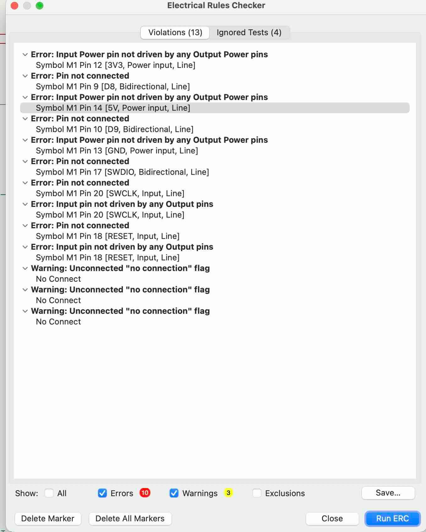
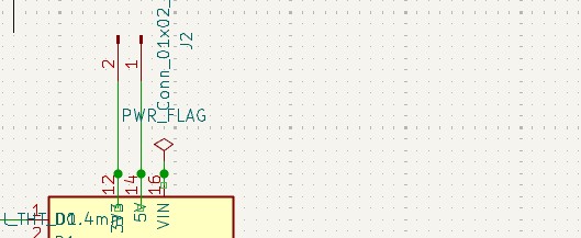
I used the PWR_FLAG symbol in the Power symbol library (press p) to solve the "Input Power pin not driven by any Output Power pins" problem by telling KiCad that the components are actually driven. I added this symbol to the VCC and GND nets and re-ran the ERC. There were still other problems that I had to work through to solve, but eventually the ERC passed without any major violations. The schematic is complete.
I opened the board editor and began arranging the footprints and drawing the traces. To import the schematic into the board editor, click Tools → Update PCB from Schematic. I pressed the button in the top toolbar, which is easier.
I only added a few pins connected to the board. The remaining unconnected pins throw an error. I used "no connect" to tell the ERB that the pin is not going to be used.
I created a pcb that will easily house and reuse the RP2040 board from Xiao, as I only have one available to me. I've added a standard mount for the board, as well as pins for power, GPIO and an LED and resistor for simple testing.
Eventually, I worked through the problems.I ran the design rules checker and received no major warnings and eight warnings.
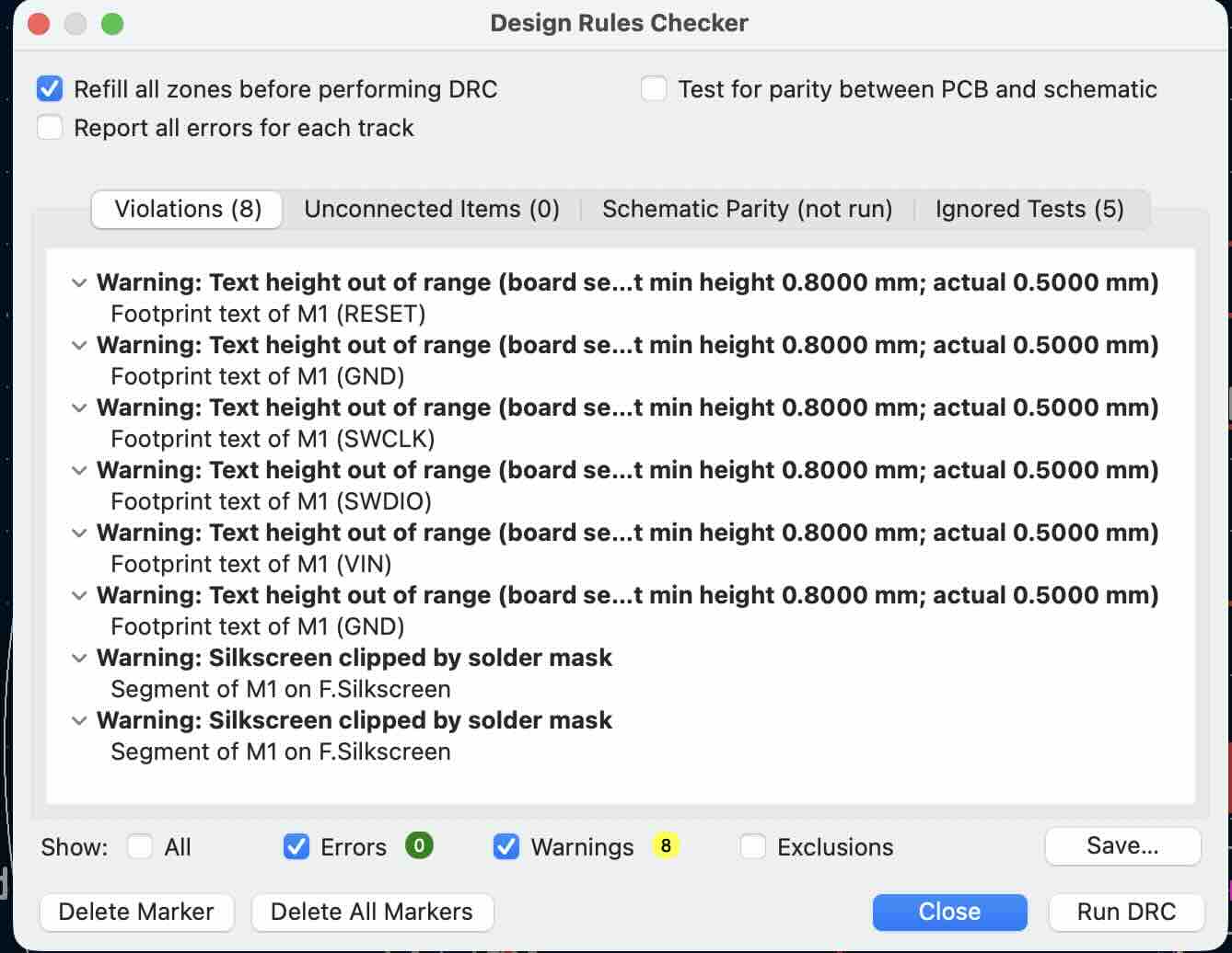
Note- I found out after this week that the traces on my board were too thin at 0.2 mm thick. A rule of thumb I was given during GOT was that traces should be at least 0.4mm thick, with power being 0.6 mm.
Note, the board had a lot of problems that I discovered after the fact. First of all, the traces were too small- they should be about 0.6mm for anything related to power. I eventually decided to throw out this design as it was not practical and, honestly, the form factor would make it hard to mount.