Assignments
Week 8 – Electronics Production
Assignments
Group assignment:
- Characterize the design rules for your in-house PCB production process
- Submit a PCB design to a board house
Individual assignment:
- Make and test an embedded microcontroller system that you designed
- Extra credit: make it with another process
Group Assignment — Lessons Learned
During the group assignment, I learned that understanding the design rules is essential to avoid machining errors. Parameters such as trace width and spacing must be carefully defined according to the tool diameter and machine capabilities. Proper calibration of the CNC machine plays a critical role in achieving accurate results. Working as a team also helped compare results, identify issues more quickly, and validate the optimal machining parameters.
🔗 If you want to explore the Group Assignment in more detail, you can visit the official Fab Academy page:
Visit Fab Academy ULima →PCB Machining Process
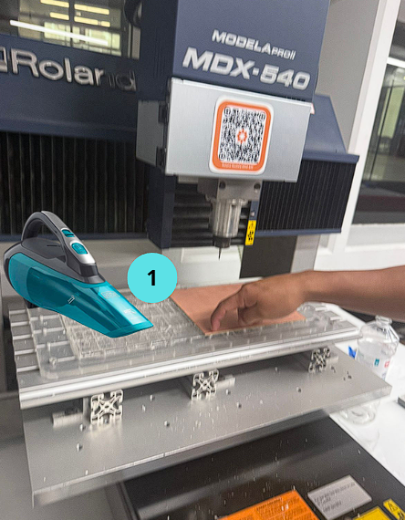
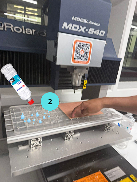
Today, I carried out the PCB machining process using the Modela Pro II MDX-540 machine.
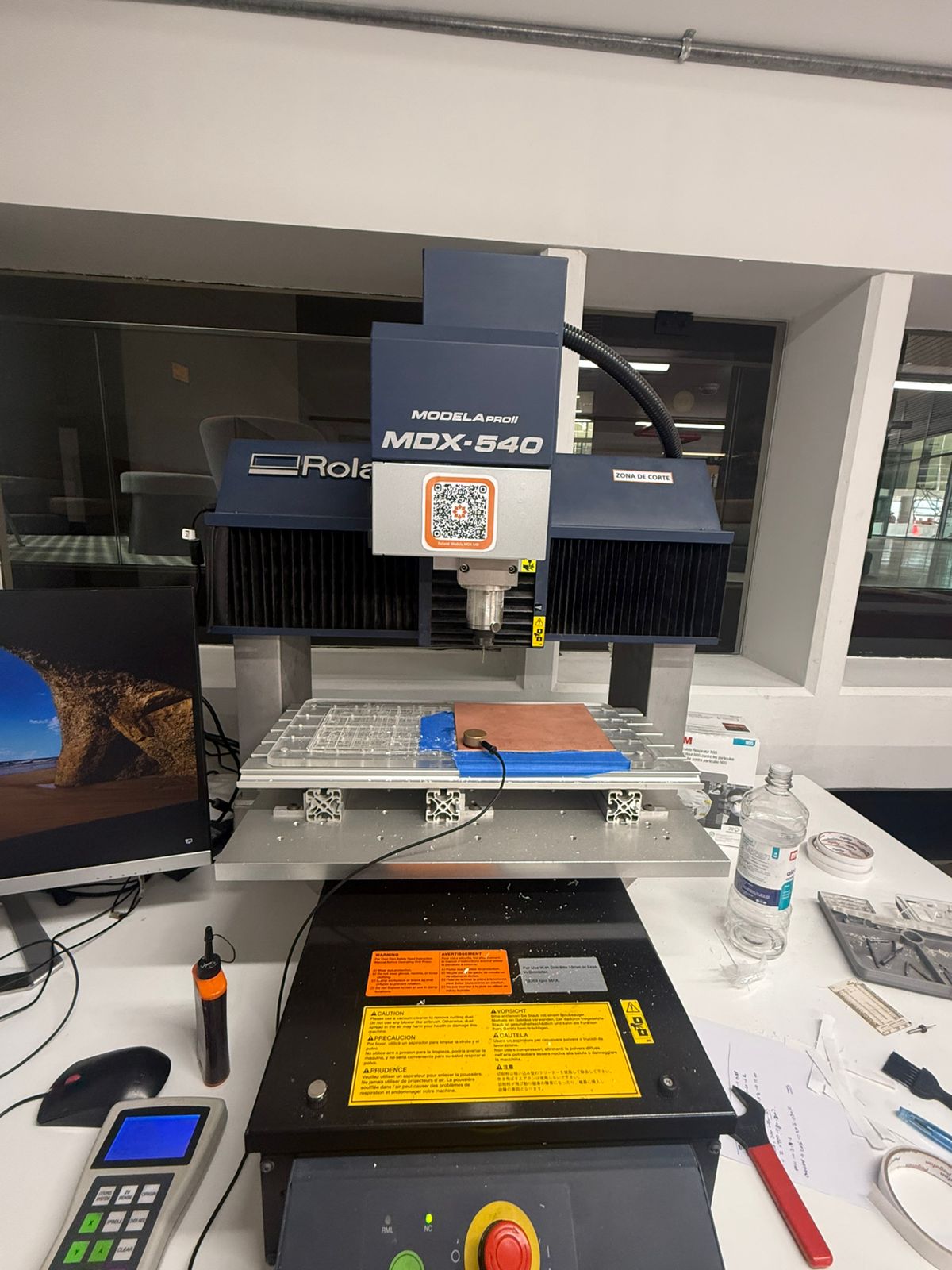
First, the machine bed was cleaned using alcohol, and any remaining debris from previous machining processes was removed. This step is essential to ensure a clean surface and avoid precision errors.
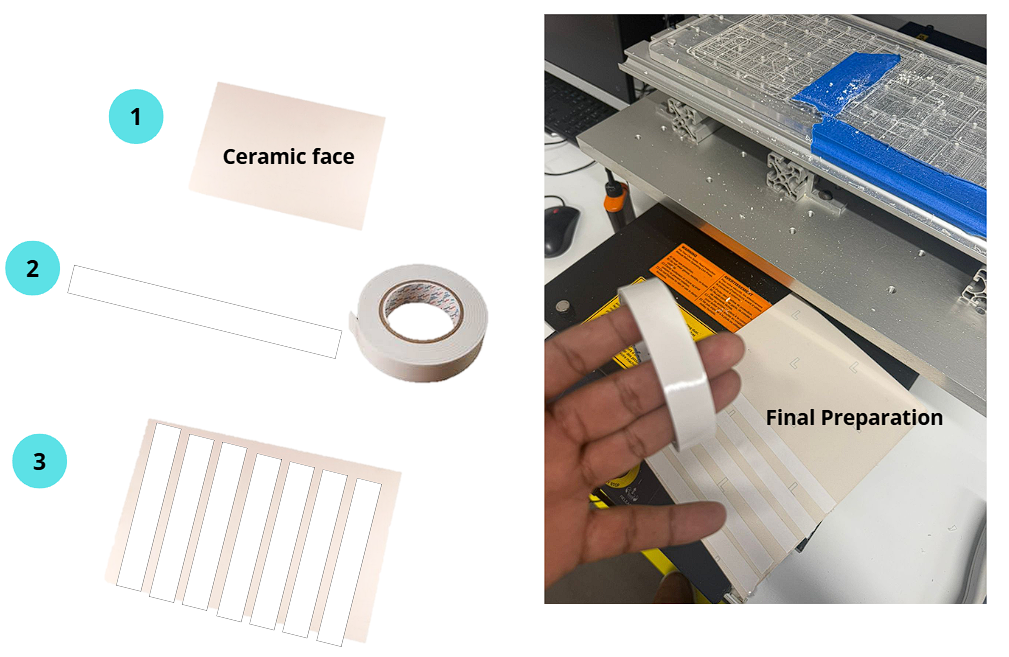
Next, the copper board was prepared by placing double-sided tape on the back side in order to fix it firmly. It is very important that the board is as flat as possible, since any unevenness can affect the depth of the engraving or cutting process.
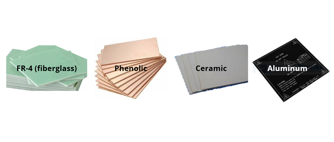
PCB Material
✅ Material Used: FR1 (Phenolic Paper)
For this project I used FR1 (phenolic paper-based) copper-clad board. FR1 was chosen because our lab uses an open CNC machine without a vacuum enclosure (the Modela Pro II MDX-540). FR4 (fiberglass) releases harmful glass-fiber dust when milled and requires proper dust extraction. FR1 produces wood-like dust that is much safer to machine in an open environment, making it the correct and recommended choice for in-house PCB milling without an enclosed vacuum system.
For reference, here is a comparison of the most common PCB substrate materials:
| Material | Composition | Open CNC safe? | Typical use |
|---|---|---|---|
| FR1 ✅ Used here | Phenolic paper | Yes | In-house PCB milling, prototypes |
| FR4 | Fiberglass epoxy | No (dust hazard) | Industry standard, requires enclosure |
| Ceramic | Ceramic substrate | No | High-freq / high-temp applications |
| Aluminum | Aluminum core | No | Power electronics, LEDs (heat dissipation) |
Photo of the FR1 board used in this assignment:
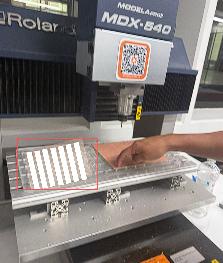
Once prepared, the board was placed on the sacrificial bed of the machine, which allows full cuts without damaging the main structure.
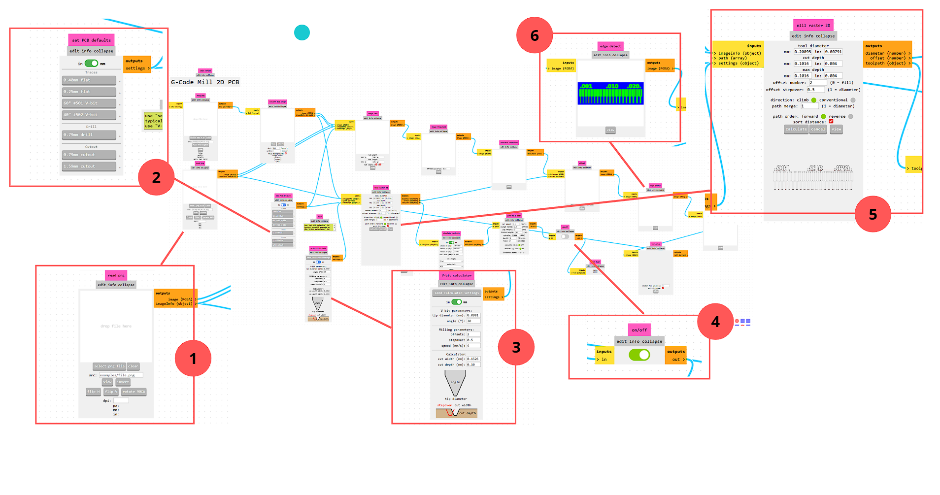
⚙️ Generating the G-code in Mods CE
To generate the G-code, I used Mods CE and connected the modules step by step. In Set PCB Defaults, I selected the 40° V-bit configuration. After defining the machining parameters, I clicked calculate to preview the result, including a 3D simulation of the toolpath and the final G-code output.
PNG Input Files
Mods CE takes PNG images as input. Below are the PNG files I used — one for the copper traces and one for the board outline. These are the same files loaded into the "Read PNG" module.
Copper traces PNG:

Board outline PNG:

Press the button according to the number
1. Read PNG
First, I loaded the PNG file of the PCB design into Mods CE as the input image for the machining workflow.
- Input: PNG file
- Available options: view, invert, flip H, flip V, rotate 90° CW
- Units: dpi, px, mm, in
Toolpath Verification
After calculating the toolpath in Mods CE, a 3D model preview was generated. To verify the result more accurately, I also used NC Viewer, loading the G-code to simulate how the PCB would be machined.
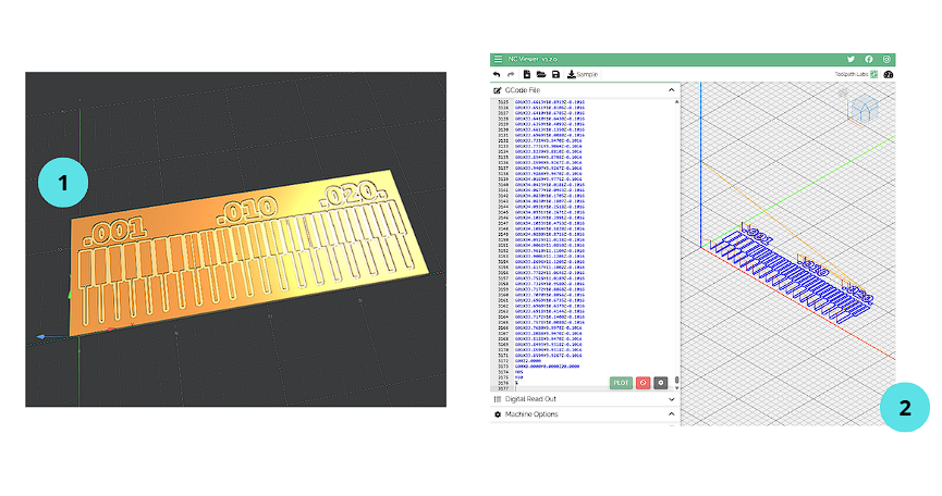
This verification step confirmed the toolpath, machining order, and general cutting behavior before running the process on the machine.
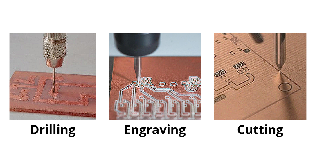
Types of PCB Machining
Engraving: The surface copper layer is removed to create the circuit traces, using fine milling tools and low depth.
Drilling: Holes are made in the board for components or mechanical fixing.
Cutting: The board is cut out, separating it completely from the base material.
Machining Process
The process started with engraving, since if cutting is done first, the board could move and lose precision.
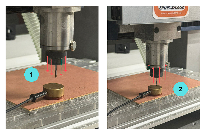
Z-Axis Calibration
After calibrating the X and Y axes, the Z-axis is calibrated using a Z-axis touch probe (sensor).
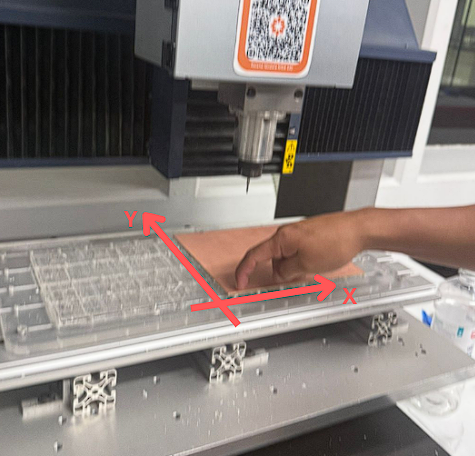
The tool is moved down until it makes contact with the sensor. Once contact is detected, the machine automatically registers the position as the reference height. The tool then moves up automatically, confirming a successful Z-axis calibration.
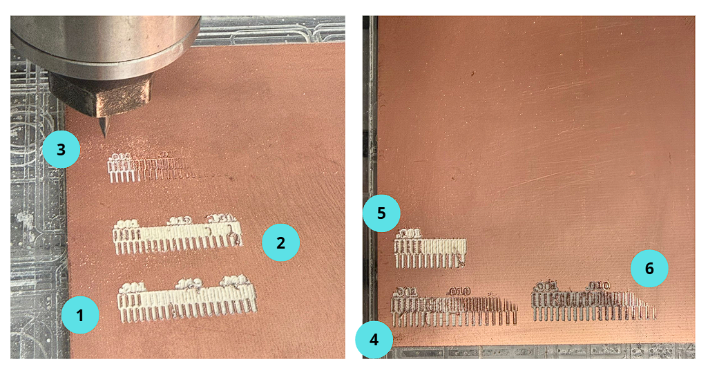
Machining Tests and Calibration
The machining tests were performed using a 2 mm V-bit tool with a Cut Z of -0.112 mm. The results showed that sensor pressure during calibration and surface leveling had a direct impact on the final machining quality.
Press the button according to the number
Attempt 1
In the first attempt, the result was not satisfactory because of an incorrect Z-axis calibration. I concluded that I pressed the sensor too much, which caused an excessive machining depth and a poor surface finish.
Individual Assignment
Individual Assignment — Lessons Learned
During the individual assignment, I realized that small variations in Z-axis calibration can significantly affect the final PCB quality. Learning how to use tools like Mods and FlatCAM was key to generating accurate G-code. The soldering process required precision, especially when working with very small SMD components, where using tweezers became essential. Proper alignment of components, particularly headers, is important to ensure correct connections, and debugging both hardware and software is an important part of the process.
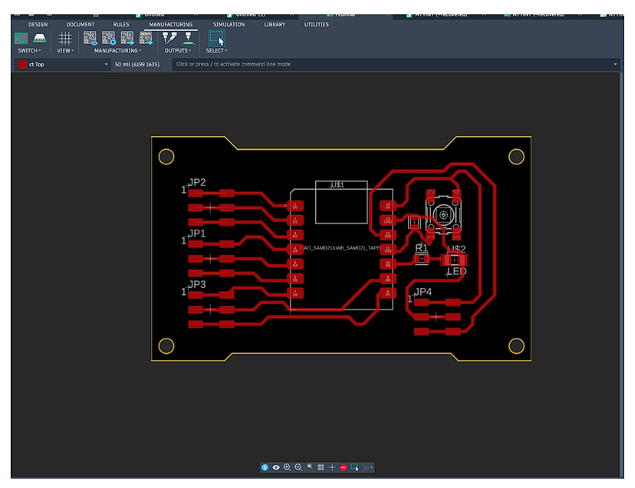
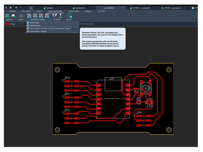
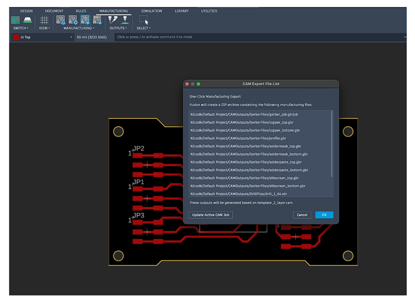
Gerber Files
Once the PCB design was completed, it was exported in Gerber format — the industry-standard format for PCB manufacturing. Gerber files can be inspected with any free Gerber viewer (e.g., Ucamco viewer, gerbv) regardless of which EDA software you use, making them the most reliable way to share and verify a PCB design.
The exported files include:
- Copper layer (.gbr) — defines all copper traces and pads
- Board outline / Edge Cuts (.gbr) — defines the physical board perimeter
Download Gerber files:
The complete schematic design and development process can be seen in Week 6 documentation.
FlatCAM — Copper
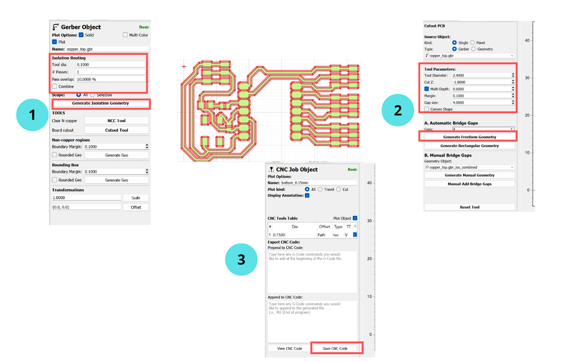
After importing the copper Gerber file into FlatCAM, I configured the isolation routing process, defining parameters such as the tool diameter, number of passes, pass overlap, and tool settings to generate the toolpath for the PCB traces.
Press the button according to the number
1. Isolation Routing
First, I configured the isolation routing to define how the copper around the traces would be removed.
- Tool dia: 0.1000
- # Passes: 1
- Pass overlap: 10.0000%
- Generate Isolation Geometry: creates the trace toolpath
FlatCAM — Profile
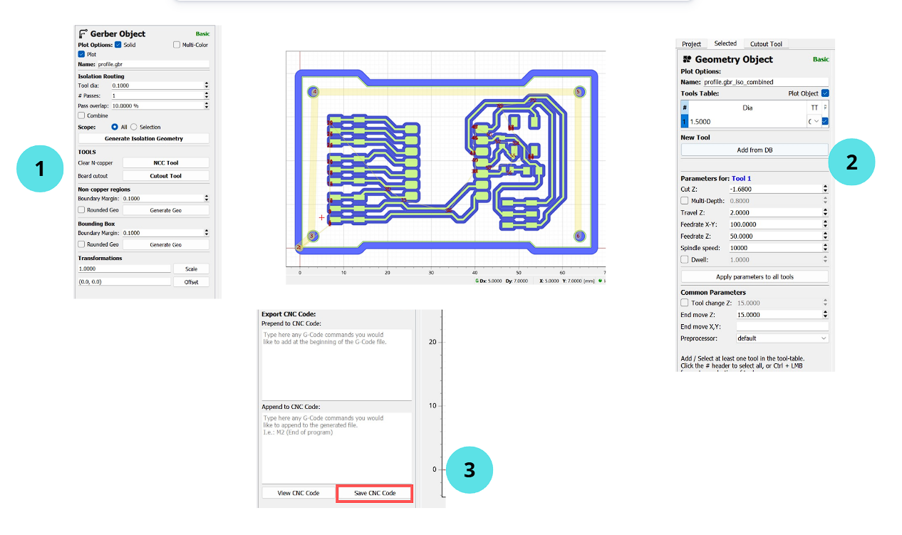
For the profile operation, I specified Cut Z, travel height, feedrate, and spindle speed to define the external board cut.
Press the button according to the number
1. Gerber Object
First, I opened the profile Gerber file and configured the geometry generation for the board outline.
- Name: profile.gbr
- Tool dia: 0.1000
- Generate Isolation Geometry: creates board path
- Board cutout: prepares external contour
PCB Assembly (Soldering)
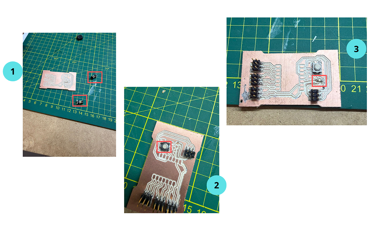
After machining the PCB, the next step was assembling the components by soldering. This process requires precision, especially when working with small SMD components.
Press the button according to the number
1. SMD Pin Headers
First, I soldered the SMD pin headers onto the PCB. These components create electrical connections between the board and external devices or modules. This step was relatively easy and did not present major difficulty.
Final Assembly Details
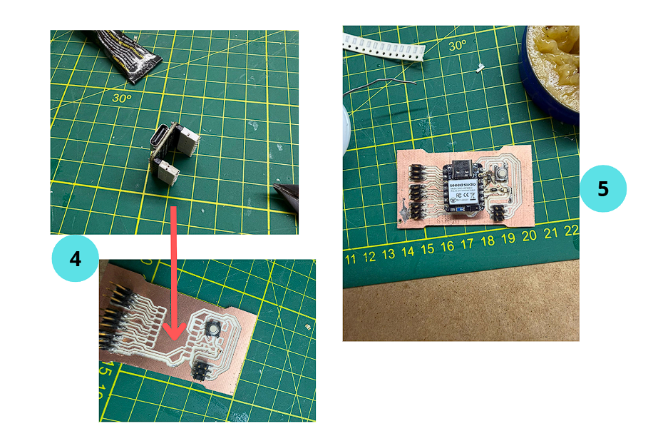
In the final stage, additional care was taken to ensure proper alignment and correct positioning of key components before completing the PCB.
4. SMD Female Headers Alignment
Before soldering the SMD female headers, I first placed them on the Seeeduino board to ensure proper alignment. If soldered freely by hand, the position may be inaccurate, affecting the connection and overall assembly.
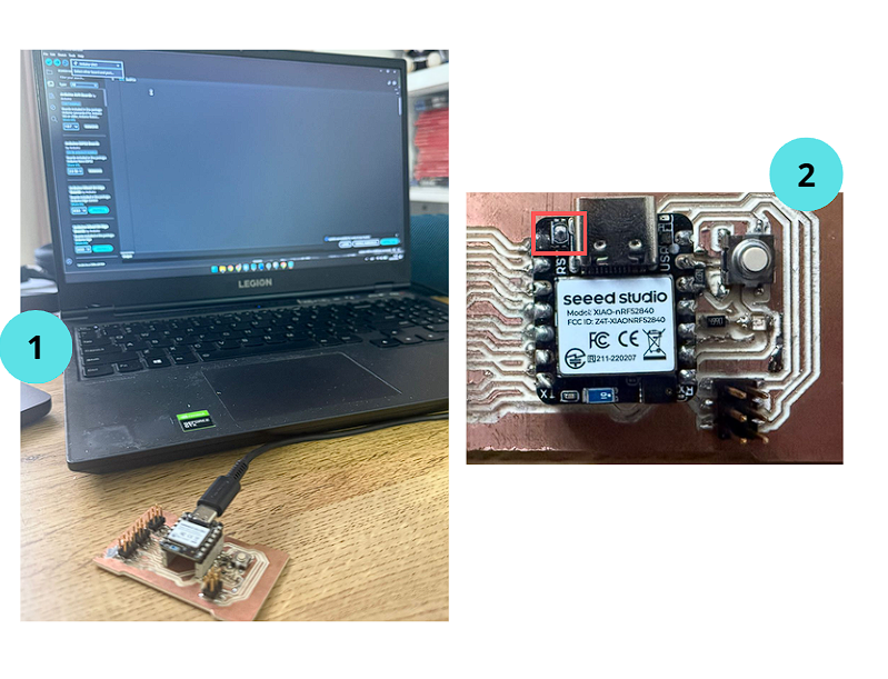
Programming Setup
Button-Controlled LED Test
In this test, an LED is turned on using a push button as input. The button is wired to pin 10 using INPUT_PULLUP — the internal pull-up resistor means the pin reads HIGH when released and LOW when pressed.
// Button-Controlled LED — custom PCB
// Pin 9: LED output | Pin 10: push button (INPUT_PULLUP)
const int led    = 9;
const int boton  = 10;

void setup() {
  pinMode(led,   OUTPUT);
  pinMode(boton, INPUT_PULLUP);  // HIGH = released, LOW = pressed
}

void loop() {
  int estado = digitalRead(boton);

  if (estado == LOW) {           // Button pressed → turn LED on
    digitalWrite(led, HIGH);
  } else {                       // Button released → turn LED off
    digitalWrite(led, LOW);
  }
}
After connecting the board, the device was not immediately recognized. Pressing the RESET button on the board forces the microcontroller into bootloader mode, allowing the computer to detect it and enabling code upload through the Arduino IDE.
Demonstration of the PCB working with button-controlled LED.
Project Downloads
Download all files related to the PCB design and fabrication:
.nc)
.nc)