Assignments
Week 6 – Embedded Programming
Assignment
Group assignment
- Use the test equipment in your lab to observe the operation of an embedded microcontroller.
Individual assignment
- Simulate a circuit.
- Use an EDA tool to design an embedded microcontroller system using parts from the inventory, and check its design rules for fabrication.
- Extra credit: Try another design workflow.
- Extra credit: Design a case.
Group Assignment – Reflection
During the group assignment, I gained practical experience using laboratory test equipment to analyze real embedded systems behavior. Working with the oscilloscope helped me observe signals in real hardware (power rails, GPIO outputs, PWM waveforms) and understand the relationship between code and electrical response. Troubleshooting the LED test reinforced the importance of voltage drops, current limitation, and real circuit conditions.
🔗 If you want to explore the Group Assignment in more detail, you can visit the official Fab Academy page:
Visit Fab Academy ULima →
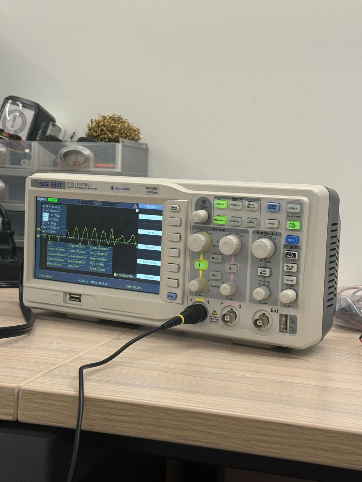
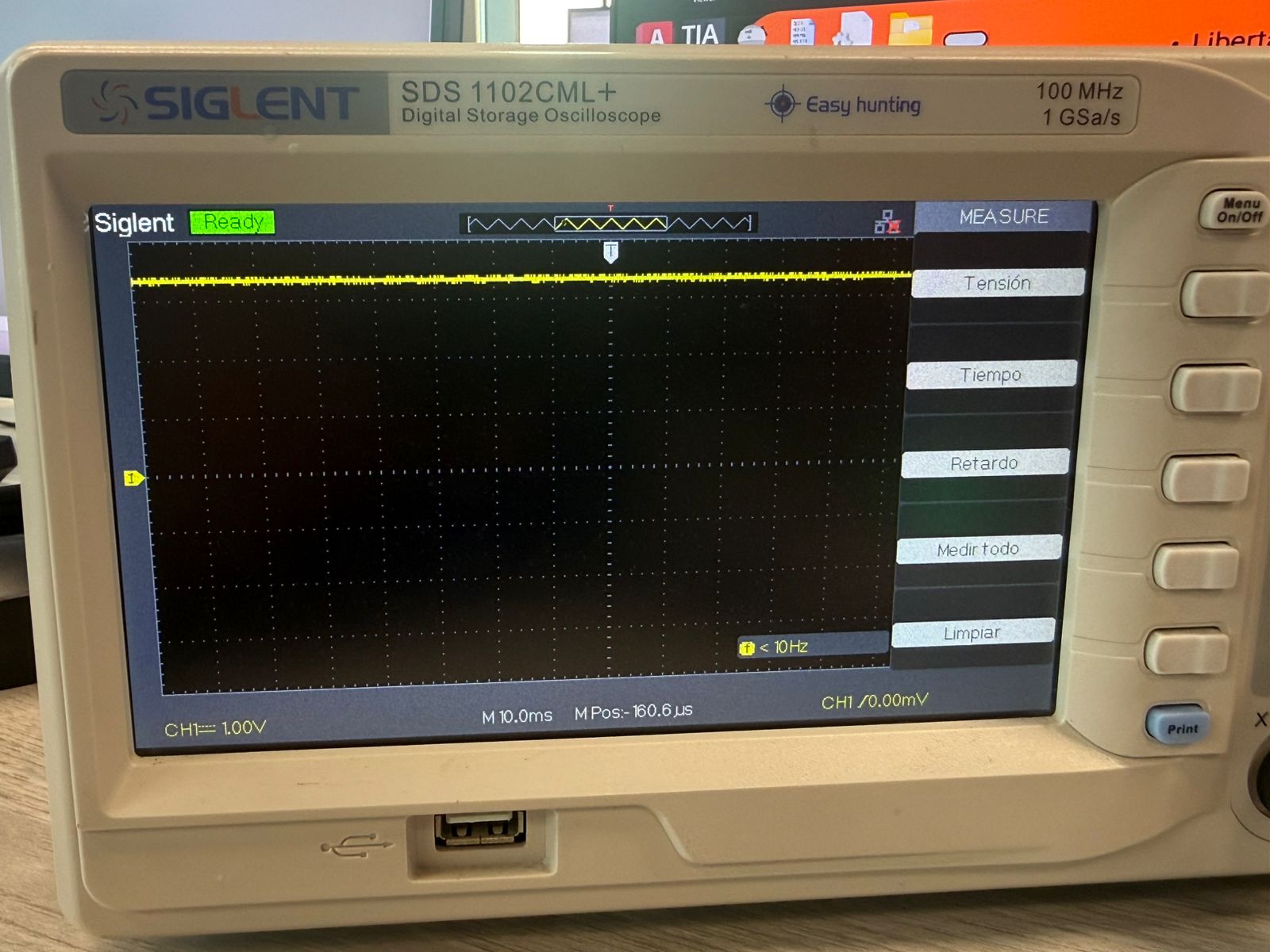
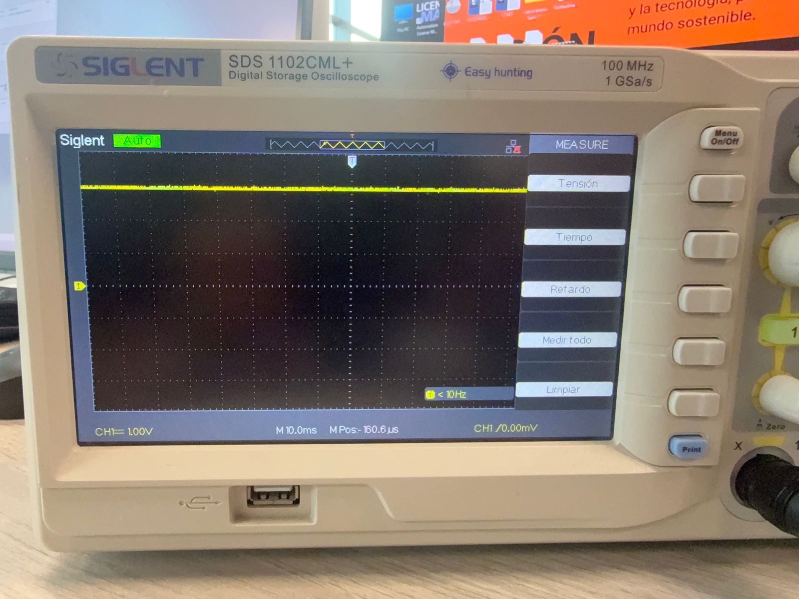
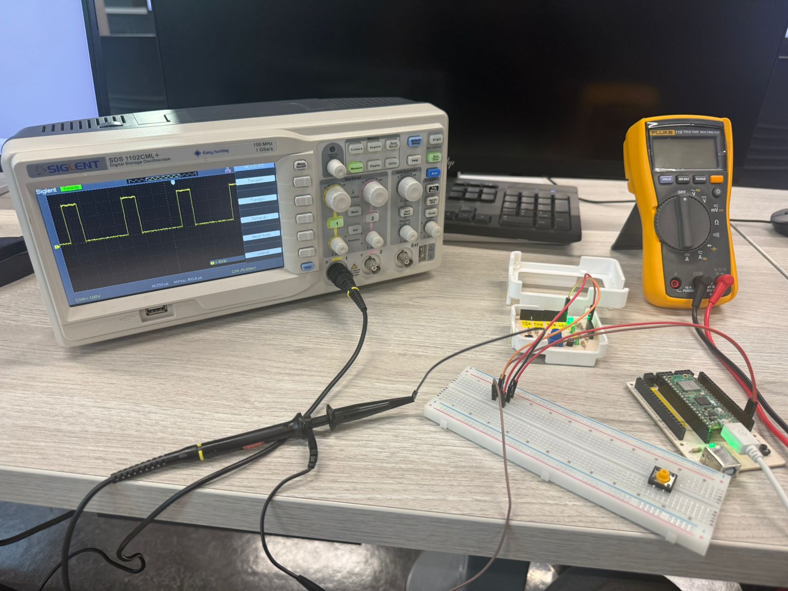
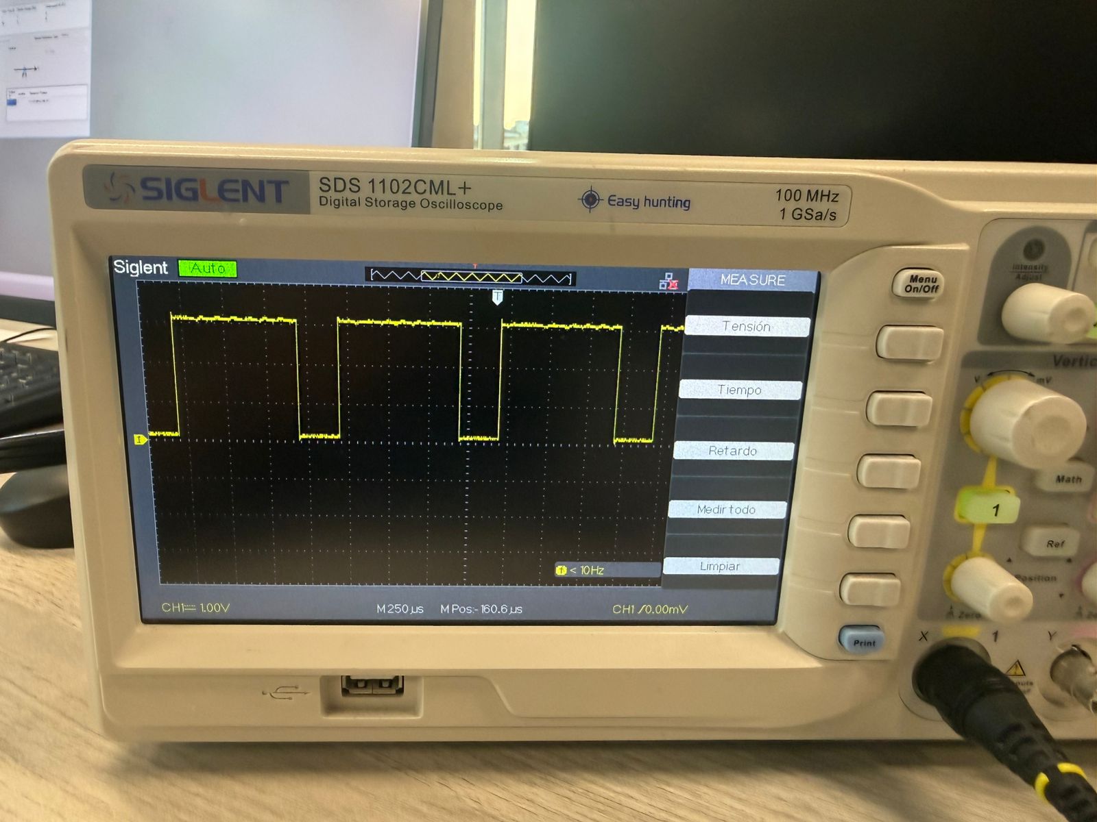
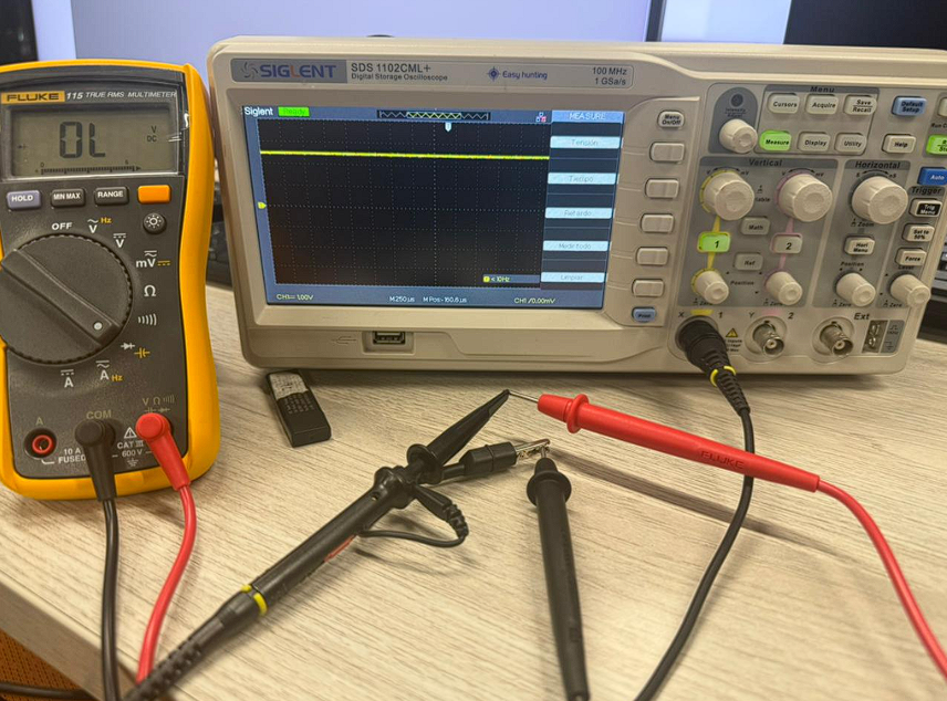
Oscilloscope – Siglent SDS 1102CML
An oscilloscope is used to visualize electrical signals over time. Unlike a multimeter, it shows the waveform, so we can analyze amplitude, frequency, period, duty cycle, and timing behavior. This is key for debugging embedded systems and confirming the output matches the program.
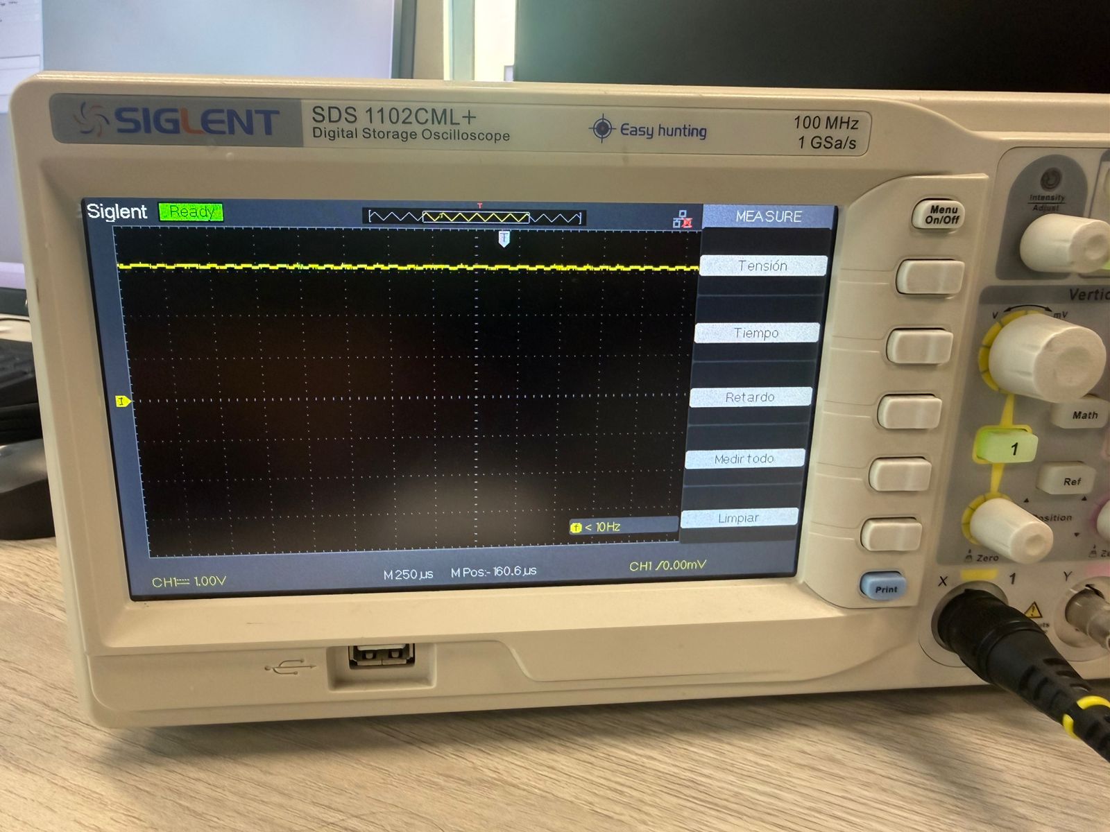
The model used was the Siglent SDS 1102CML. It is useful for digital signals (HIGH/LOW), PWM signals, and verifying correct timing and stability in microcontroller outputs.
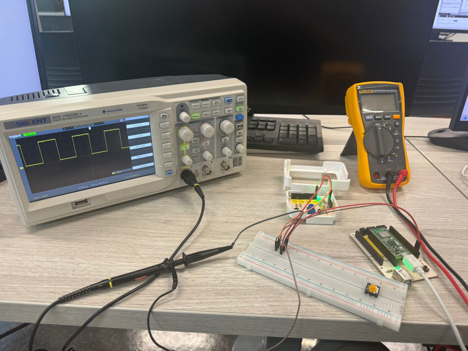
Test 1 – Voltage Measurements (Oscilloscope)
The board was powered by USB (5V). The onboard regulator provides a stable 3.3V rail for the microcontroller. Measuring the 3V3 pin confirmed correct regulation (3.3V).
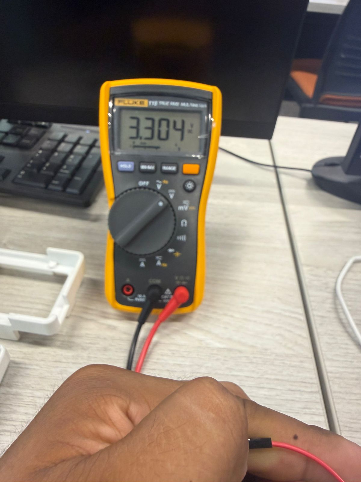
Then we measured a GPIO header related to GPIO 1 and got around 2.9V. This happens because the GPIO was also driving an LED load, producing a small voltage drop at that point, while the main 3.3V rail remained stable.
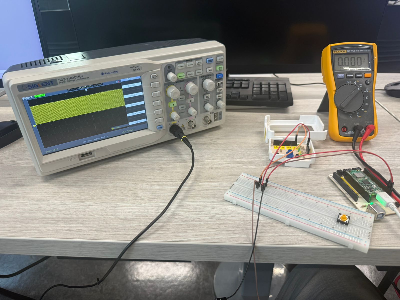
Test 2 – PWM Duty Cycle and LED Behavior
We tested PWM at 25%, 50%, 75%, and 100% to see how duty cycle affects brightness (average power delivered to the LED).
25%: dimmer (ON for a short time).
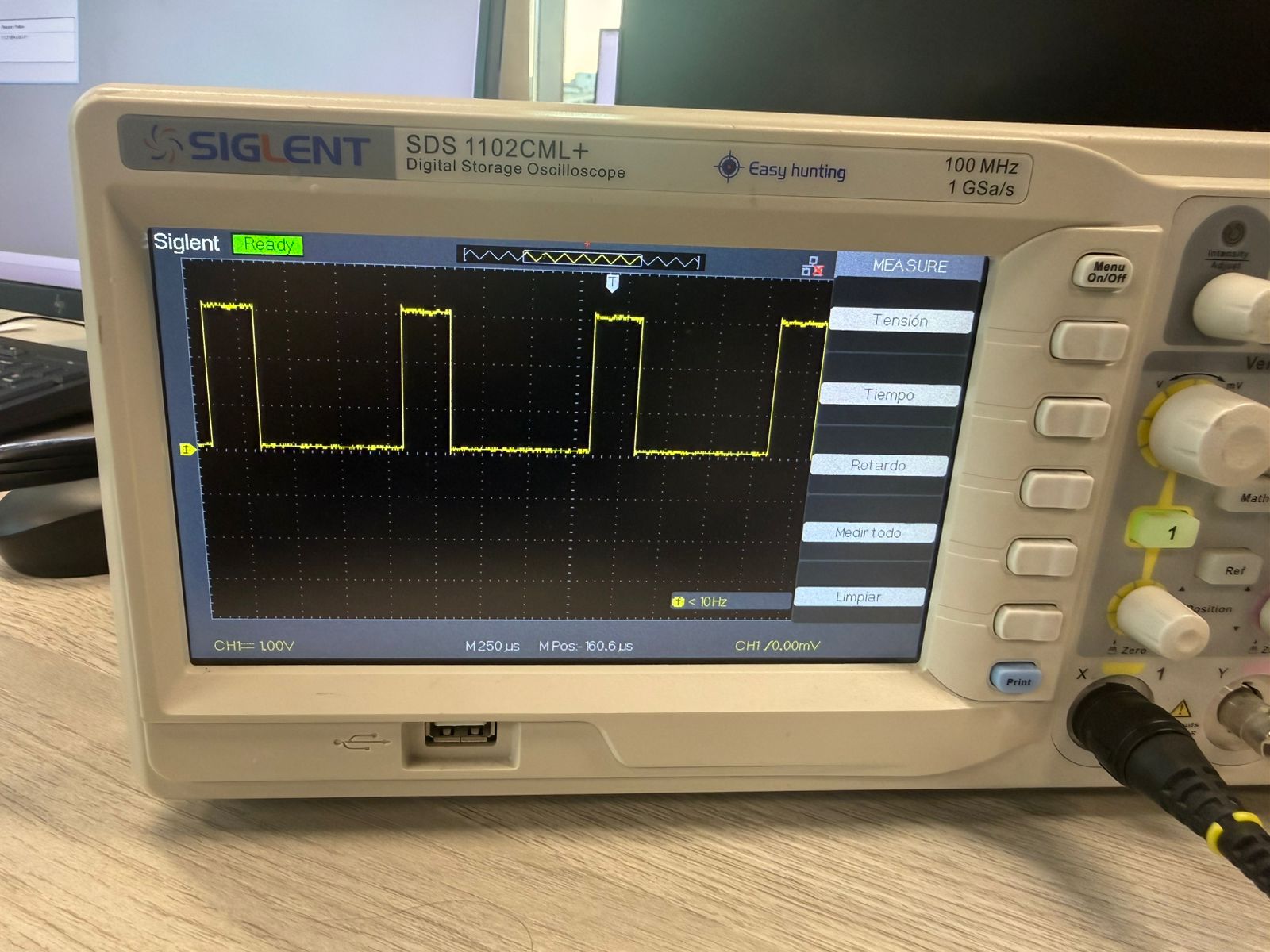
50%: brighter (ON for half the period).
75%: close to max brightness.
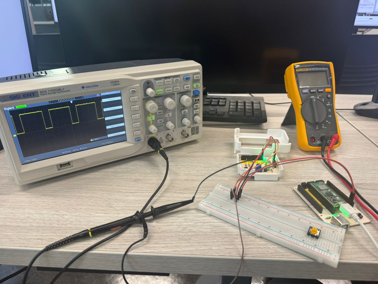
100%: constant HIGH (acts like DC).

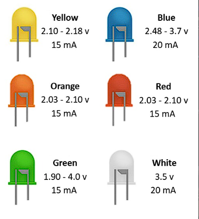
LED - Diode Test and Signal Analysis
The multimeter was set to diode mode to verify several LEDs. Most illuminated, confirming polarity and basic functionality. One red LED did not turn on as expected, so we checked conditions more carefully.
LED Forward Voltage by Color
LEDs have a forward voltage (Vf) depending on color/material. Red/orange/yellow often work around 2.0–2.2V, while blue/white usually need 2.8–3.7V. Even if voltage is enough, the LED may not light if current is too low. A series resistor is required to keep current safe and stable.
Individual Assignment
For this individual assignment, I designed a custom embedded PCB
using Autodesk Fusion Electronics. The objective was understanding
the complete workflow of PCB development, starting from electronic
simulation and schematic creation to PCB routing, component
organization, and final board customization.
Before creating the PCB, I first explored how electronic components
behave through simulations and basic circuit testing. This helped me
better understand voltage, current flow, digital inputs/outputs,
PWM signals, analog inputs, and I2C communication before starting
the final embedded board design.
1. Exploring Microcontroller Functionalities Through Simulations
Before starting the PCB design, I first explored some of the main functionalities that can be implemented using a microcontroller. These simulations helped me better understand digital inputs, digital outputs, PWM control, analog reading, and I2C communication before designing the final embedded board.
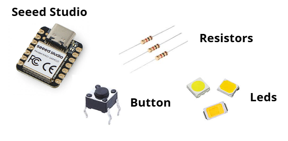
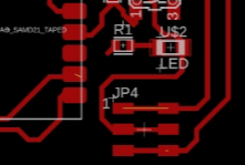
For the final PCB, I decided to integrate:
- XIAO SAMD21 microcontroller
- Push button as digital input
- LED as visual output
- 220 Ω resistor for LED current limiting
- 1 kΩ resistor for button stabilization
Press a button to explore each simulation exercise.
Exercise 1 – Push Button Controlling an LED
The first simulation consisted of controlling an LED using a push button. This basic test demonstrates how a microcontroller can read a digital input and control a digital output.
const int led = 9;
const int boton = 10;

void setup() {
  pinMode(led, OUTPUT);
  pinMode(boton, INPUT);
}

void loop() {
  int estado = digitalRead(boton);

  if (estado == HIGH) {
    digitalWrite(led, HIGH);
  } else {
    digitalWrite(led, LOW);
  }
}
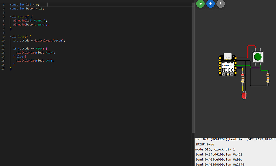
Push button controlling an LED using digital input and output logic.
Exercise 2 – Displaying Button State on an I2C LCD
The second simulation introduced an I2C LCD display to visualize the state of both the push button and the LED. This experiment helped me understand basic I2C communication and user feedback systems.
#include <Wire.h>
#include <LiquidCrystal_I2C.h>

const int led = 9;
const int boton = 10;

LiquidCrystal_I2C lcd(0x27,16,2);

void setup() {
  pinMode(led, OUTPUT);
  pinMode(boton, INPUT);

  lcd.init();
  lcd.backlight();
}

void loop() {
  int estado = digitalRead(boton);
  digitalWrite(led, estado);

  lcd.setCursor(0,0);
  lcd.print("Boton: ");
  lcd.print(estado ? "ON " : "OFF");

  lcd.setCursor(0,1);
  lcd.print("LED: ");
  lcd.print(estado ? "ON " : "OFF");

  delay(100);
}
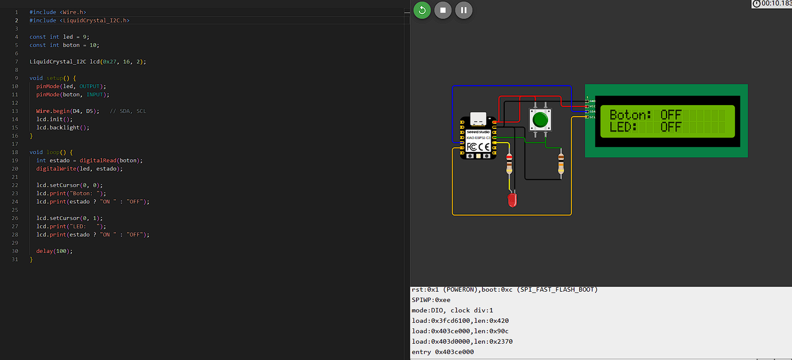
LCD interface integrated with the button and LED system.
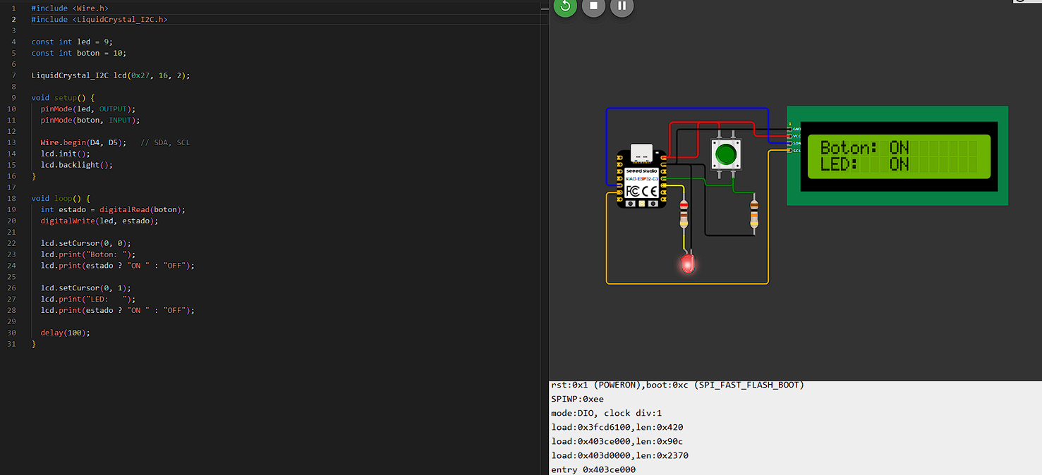
Displaying the button and LED state using I2C communication.
Exercise 3 – Potentiometer Controlling LED Brightness
The third simulation used a potentiometer as an analog input. The analog value was mapped into a PWM signal to control LED brightness dynamically.
const int led = 9;
const int pot = A0;

void setup() {
  pinMode(led, OUTPUT);
}

void loop() {
  int valor = analogRead(pot);
  int brillo = map(valor, 0, 4095, 0, 255);
  analogWrite(led, brillo);
}
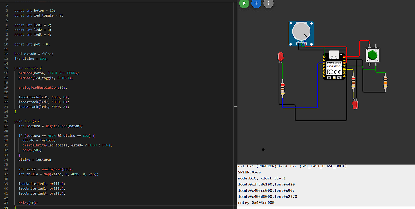
PWM brightness control using a potentiometer as analog input.
2. Starting the PCB Workflow in Fusion Electronics
After understanding these microcontroller functionalities through simulations, I started the PCB design workflow using Autodesk Fusion Electronics.
Autodesk Fusion Electronics interface used for PCB development.
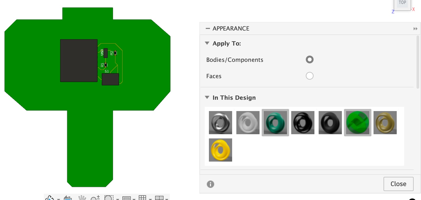
Autodesk Fusion Electronics allows creating electronic schematics, PCB layouts, routing traces, and visualizing the final board in both 2D and 3D environments.
Using the ADD command to insert electronic components.
3. Adding Components from the Fab Academy Library
The electronic components were selected using the Fab Academy library. This library already contains predefined schematic symbols and PCB footprints commonly used in Fab Academy projects.
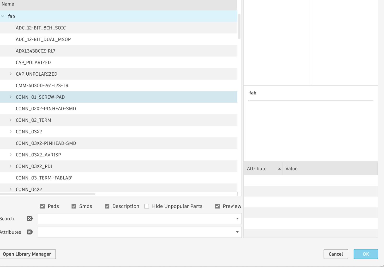
Fab Academy component library inside Fusion Electronics.
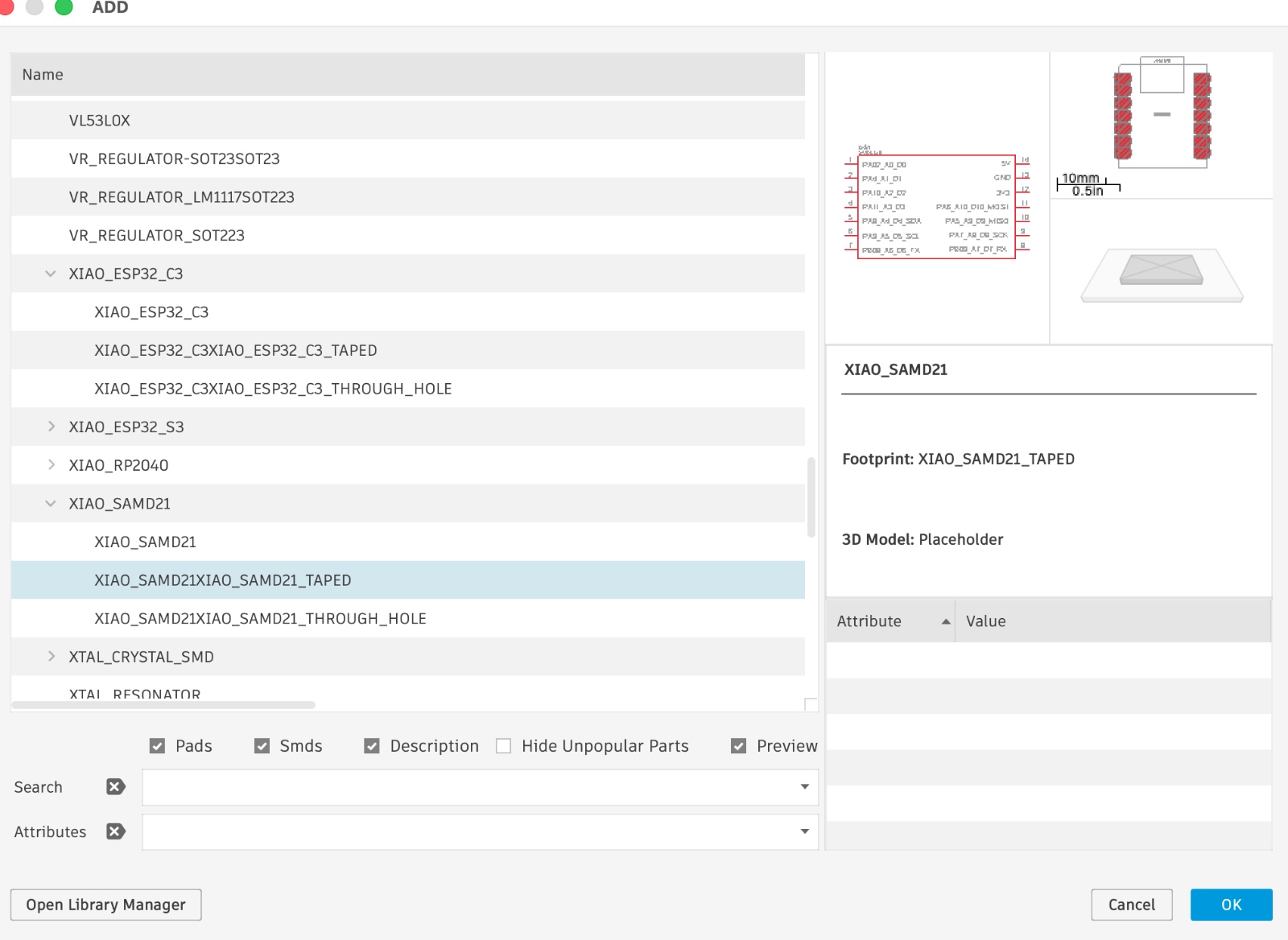
Selecting the XIAO SAMD21 microcontroller for the PCB.
4. Schematic Design
Once all components were inserted into the schematic workspace, the next step was connecting them according to the electronic design requirements.
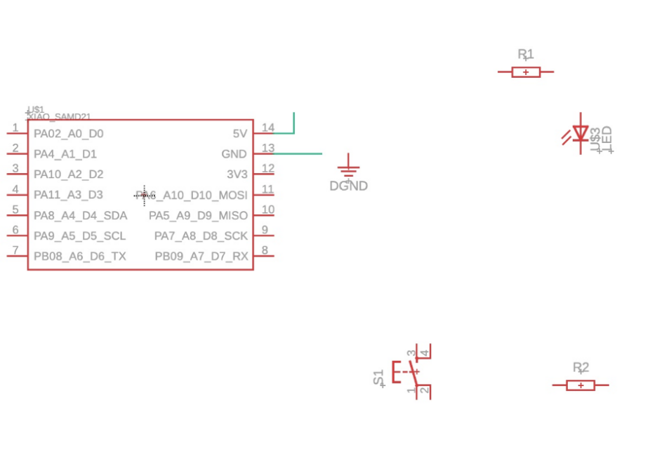
The resistor acts as a pull-down resistor, creating a defined voltage reference for the digital input pin. Without this resistor, the input could float between HIGH and LOW states due to electrical noise, causing unstable readings in the microcontroller.
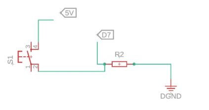
At this stage, the schematic represents the logical electronic connections of the PCB, including power lines, digital inputs, outputs, and external headers.
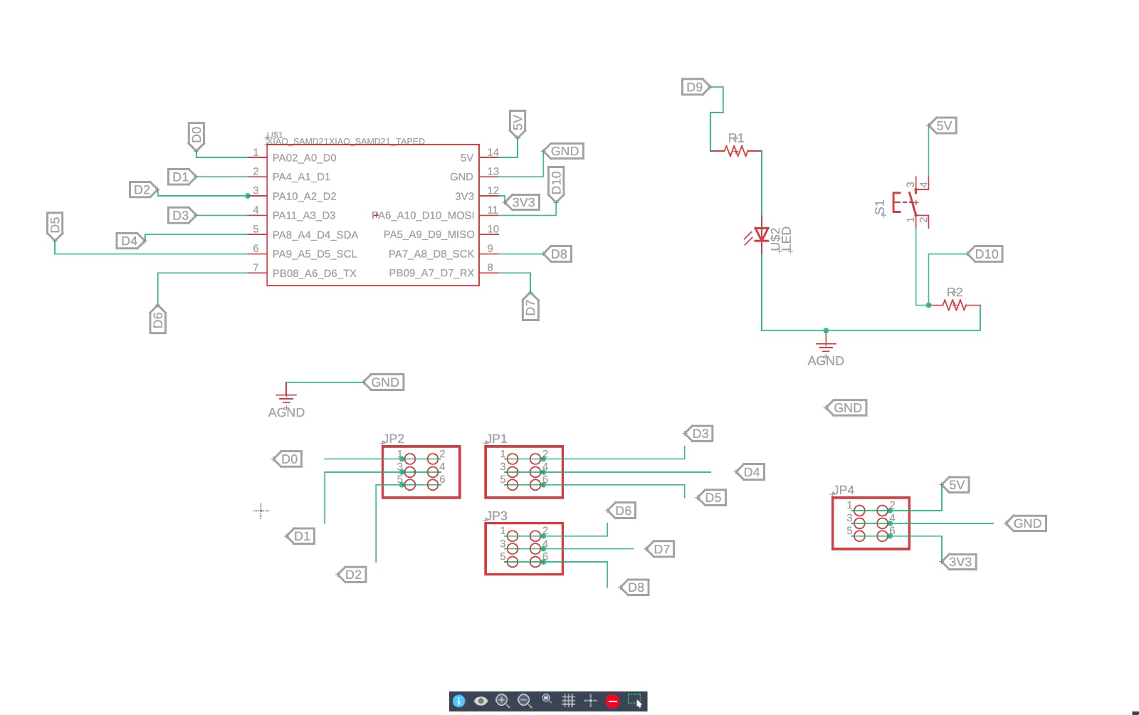
Final electronic schematic containing the XIAO SAMD21, button, LED, resistors, and external headers.
5. Converting the Schematic into a PCB Layout
After finishing the schematic, the design was converted into a PCB layout. Initially, all components appeared grouped together with unrouted airwires.
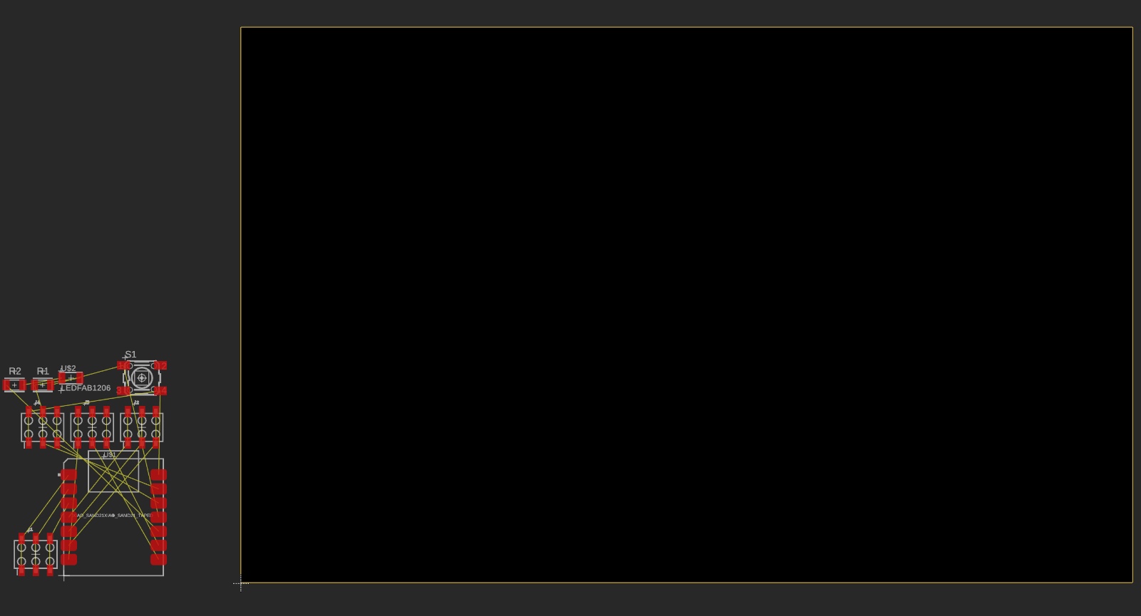
These yellow lines represent the electrical connections that still need to be routed manually.
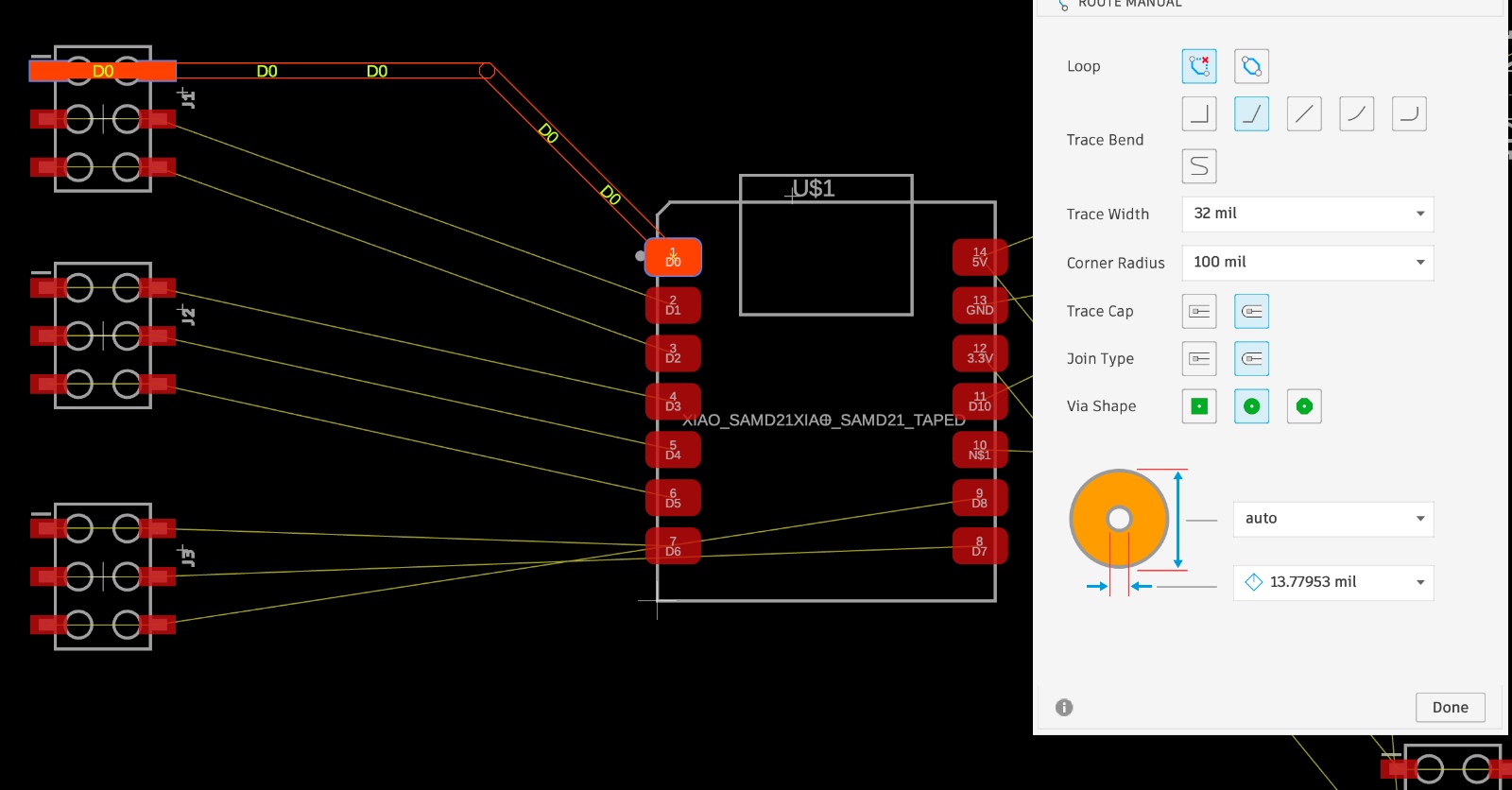
Initial PCB layout automatically generated from the schematic.
6. Organizing the PCB Components
The next step was manually organizing all PCB components to improve routing paths, reduce trace intersections, and create a cleaner and more compact design.
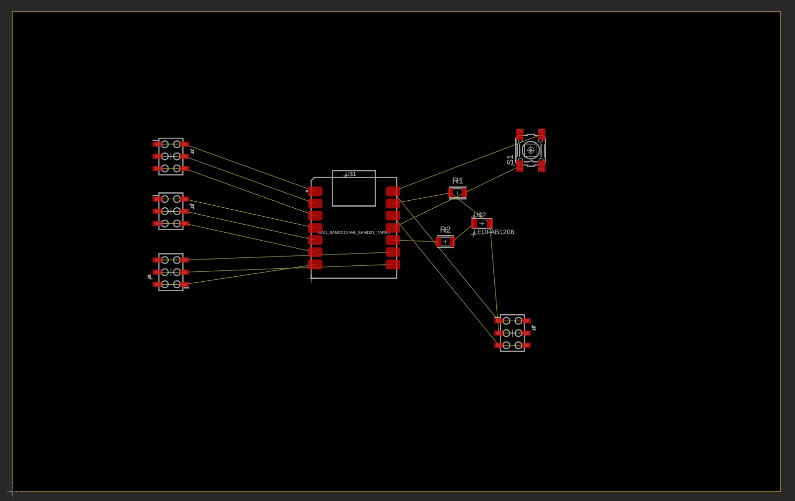
PCB components organized before starting the routing process.
7. PCB Routing and Board Shape
After organizing the components, the traces were routed manually following the airwire connections. Finally, I customized the PCB outline to create a more personalized design inspired by Mjolnir.
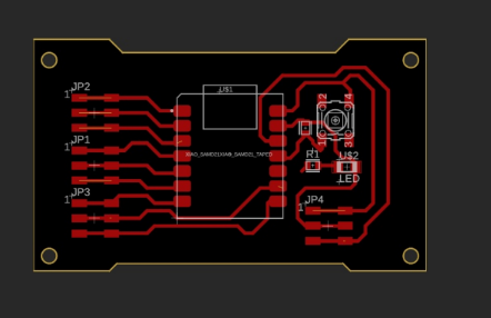
Routed PCB layout after completing the electronic connections.
Custom Mjolnir-inspired PCB shape.
Design Rule Check (DRC)
When running DRC, warnings appeared because some decorative lines were not connected to any net. The tool reads them like traces, so it reports them as “not connected”.
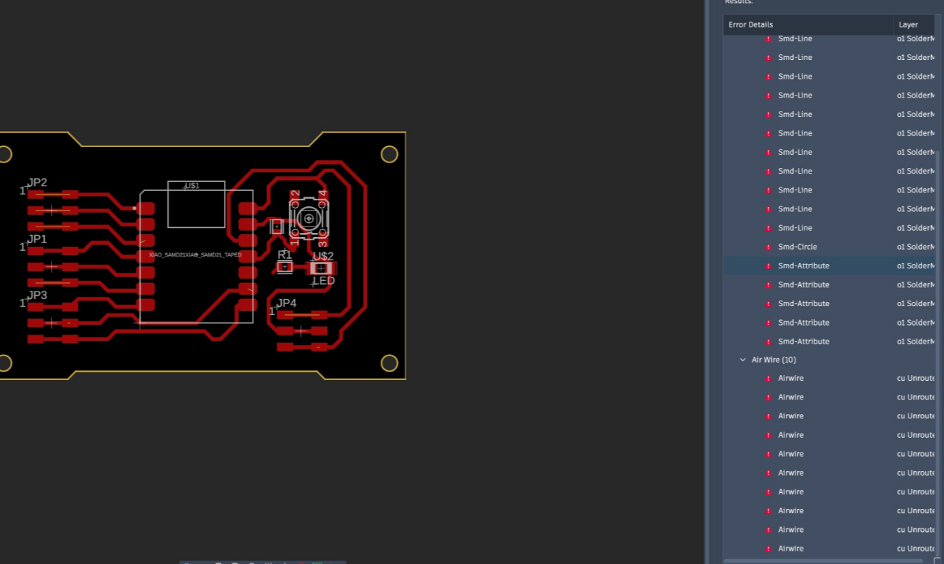
After confirming the real circuit connections were correct (LED + button + power), the warning list was cleared using Clear All.
Initial PCB Design and Issues
My first idea was a larger board to use leftover copper (less waste). But I changed to a smaller board because the first version still removed too much copper during milling.

I had two main problems: (1) I confused some pin header assignments, and (2) while labeling nets, I accidentally deleted one label, which caused missing connections.
PCB Layout and Detected Errors
Because of the wrong pin mapping and the missing label, the PCB showed airwires (unrouted connections) and multiple DRC messages. These errors basically mean: “there are nets that should be connected, but they are not routed or not recognized”.
I fixed the pin assignments and restored the missing net label. After that, I routed the traces again until all required nets were connected properly.
Project Downloads
Download all files related to the cube generation and STL models:
Test – PWM Simulation and Signal Analysis
Power Supply Reference (DC Measurement)
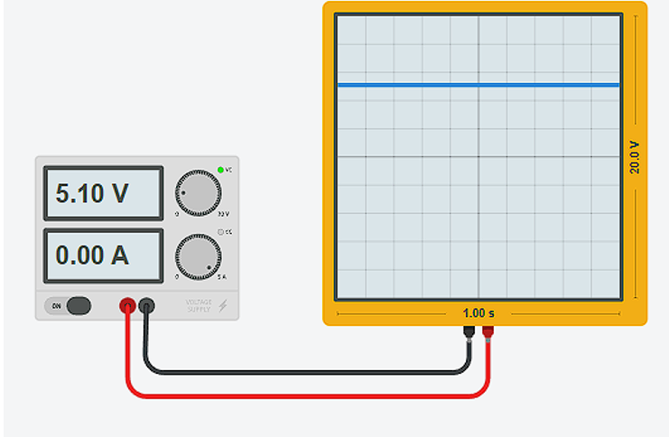
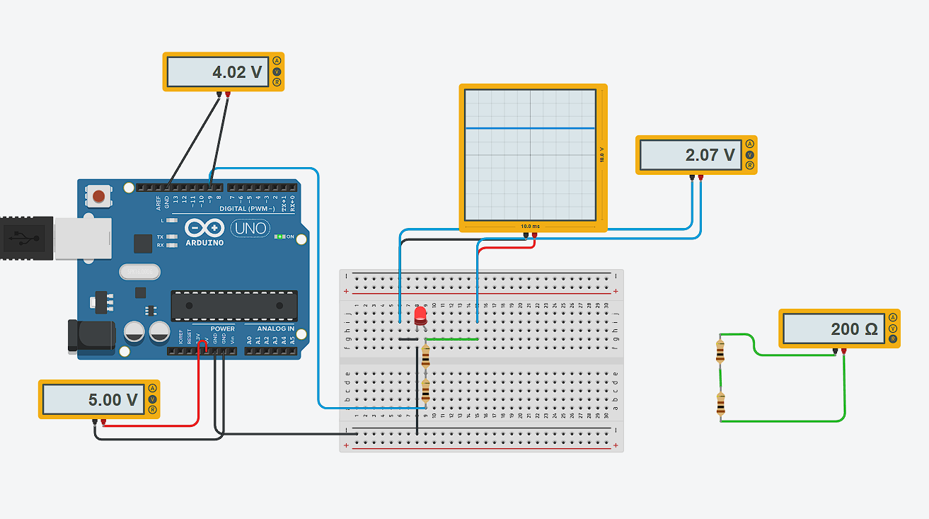
Before analyzing PWM signals, I first connected a regulated DC power supply directly to the oscilloscope. The objective was to observe how a constant voltage behaves over time and use it as a reference for comparison.
When a stable DC voltage is applied, the oscilloscope displays a horizontal flat line because the voltage does not vary with time. Unlike PWM signals, which alternate between HIGH and LOW states, a DC signal remains constant.
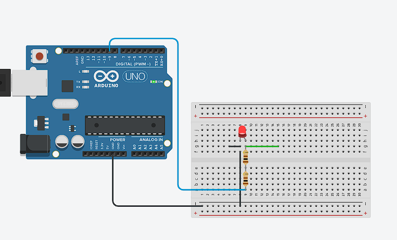
Arduino - LED Basic Circuit
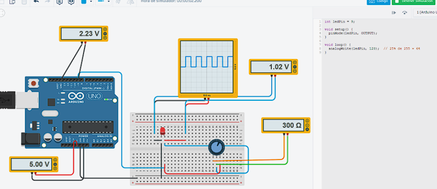
I assembled a simple circuit using an Arduino Uno, a red LED, and a 200 Ω resistor connected in series. The LED was connected to a PWM digital pin and to GND through the resistor to limit current and protect the component.
I = (Vsource − Vf) / R
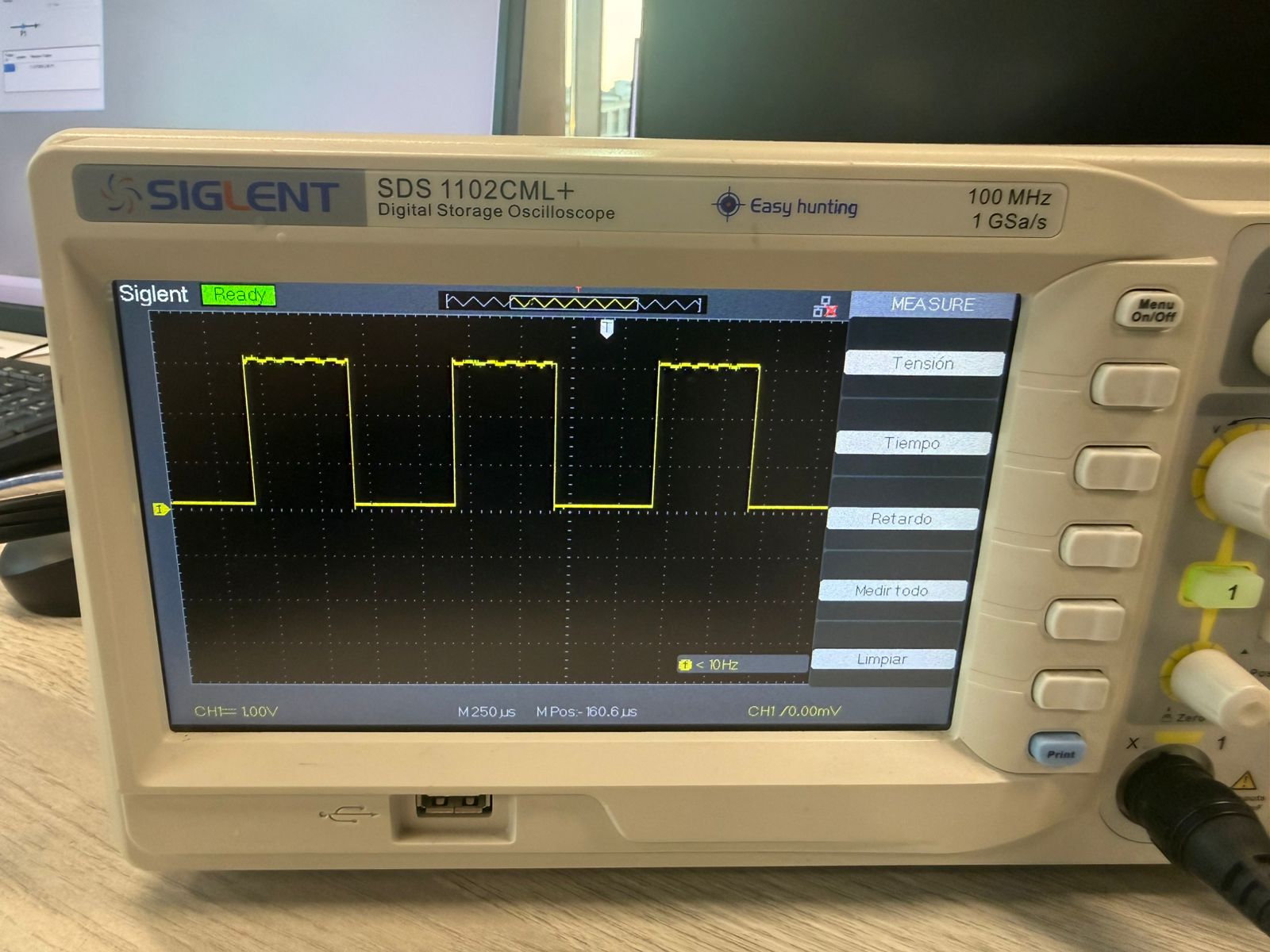
Arduino - PWM Signal Measurement
Then, I connected the oscilloscope to the PWM output pin. The signal observed was a square wave switching between 0V and 5V.
The multimeter measured the average voltage of the PWM signal. The LED showed a forward voltage of approximately 2V, while the resistor controlled the current in the circuit.
PWM Duty Cycle Analysis
PWM (Pulse Width Modulation) controls the average voltage delivered to a load by modifying the percentage of time the signal remains HIGH within one period.
Duty Cycle (%) = (Ton / T) × 100
Vavg = Duty × Vmax
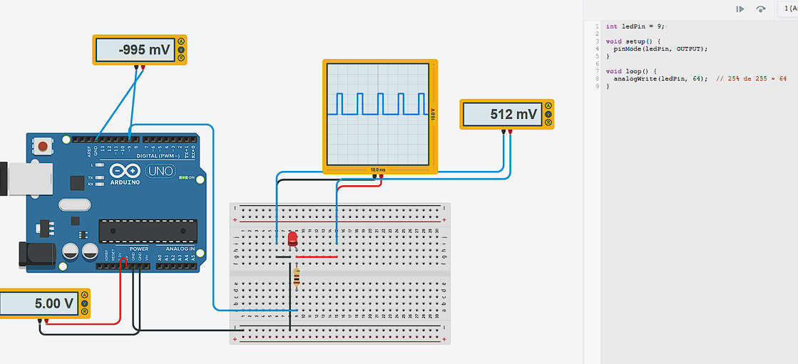
25% Duty Cycle
analogWrite(ledPin, 64);At 25%, the signal stays HIGH only one quarter of the period. The oscilloscope shows narrow pulses, and the LED appears dim because the average delivered energy is low.
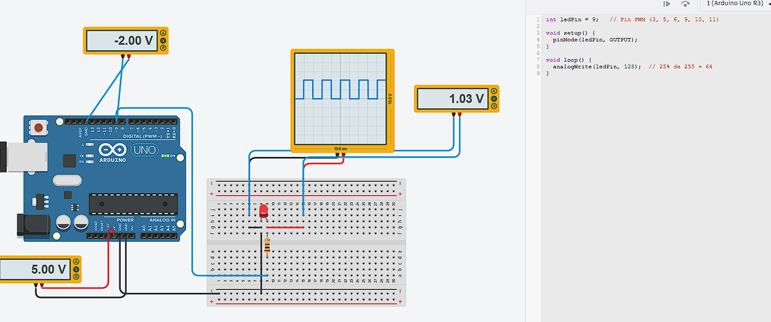
50% Duty Cycle
analogWrite(ledPin, 128);At 50%, HIGH and LOW durations are equal. The waveform shows symmetric pulses, and LED brightness increases because the average voltage is higher.
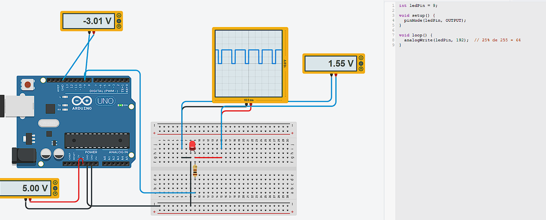
75% Duty Cycle
analogWrite(ledPin, 192);At 75%, the HIGH portion dominates most of the period. The LED brightness is significantly stronger, and the oscilloscope shows wider pulses.
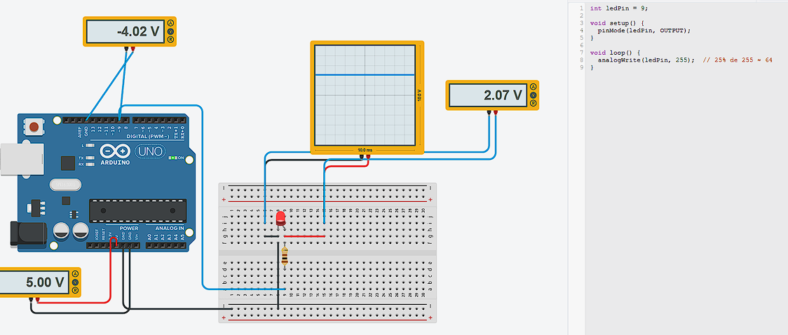
100% Duty Cycle
analogWrite(ledPin, 255);At 100%, the signal becomes constant HIGH (pure DC). The oscilloscope displays a flat line at 5V, and the LED reaches maximum brightness.
Potentiometer Behavior (Variable Resistance)
When using the potentiometer, it acted as a variable resistor connected in series with the LED, modifying the total resistance of the circuit. As the potentiometer was adjusted (around 300 Ω), the resistance changed and directly affected the current flowing through the LED according to Ohm’s Law.
I = (Vsource − Vf) / Rtotal
When the resistance increases, the current decreases (LED dimmer). When the resistance decreases, the current increases (LED brighter). This confirms that LED brightness depends mainly on current, not directly on voltage.
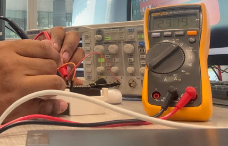
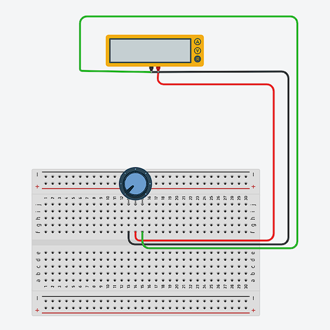
Potentiometer Test (Resistance and Voltage Range)
A potentiometer was tested to understand how its resistance changes with rotation and how it can be used either as a variable resistor or as a voltage divider.
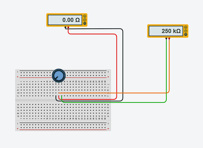
Resistance Measurement (Ohms)
When the wiper was rotated fully to one side, the measured resistance dropped close to 0 Ω. When rotated to the opposite extreme, the reading reached approximately 250 kΩ.
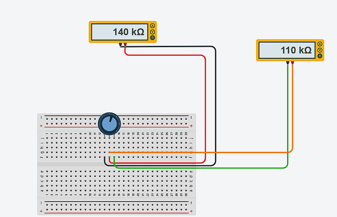
At intermediate knob positions, values around 140 kΩ and 110 kΩ were observed, confirming continuous adjustment across its full range.
Voltage Divider Behavior (Max = 3.3 V)
When used as a voltage divider, the output at the wiper varies from 0 V up to the supply voltage. Since the system was supplied with 3.3 V, the maximum measured output was also 3.3 V.
Video Demonstration
Simulation – LED Voltage/Current vs Supply Voltage
A series of simulations were performed to observe how LED current and voltage behave when changing the power supply and resistor conditions.
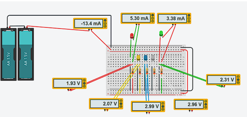
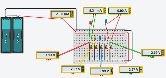
Case 1 – 2×AA Batteries (≈3.0 V)
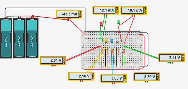
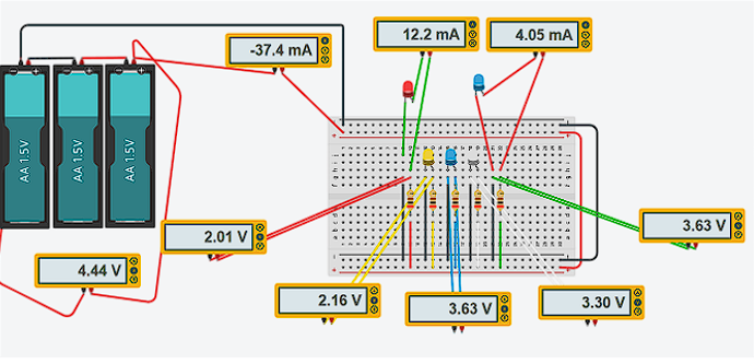
Case 2 – 3×AA Batteries (≈4.5 V)
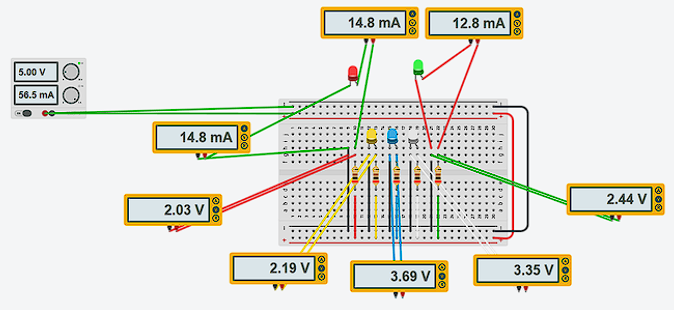
Case 3 – Regulated Bench Supply (5.0 V)
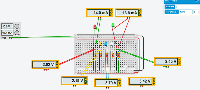
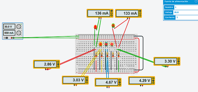
Case 4 – High Voltage (30 V) Without Proper Current Limiting
Case 5 – High Voltage (30 V) With Current Limiting (2 kΩ)