Group Assignment
Etching VS Milling, Why the difference?
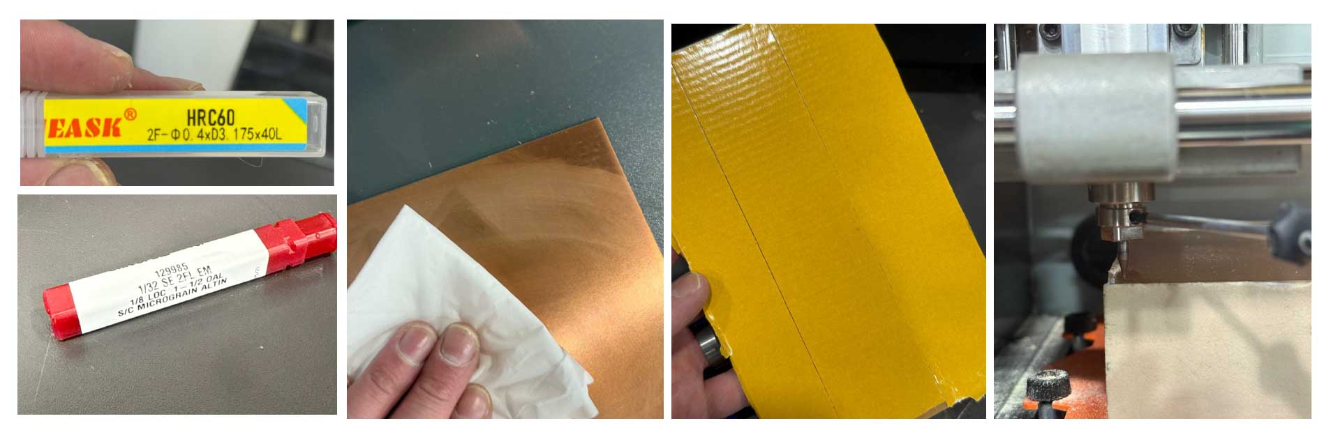
(Milling) : Because it is paper-based, it is soft enough for mechanical bits to carve away the copper without ruining the tools.
(Etching) : Because the fiberglass core is so abrasive, industrial manufacturers prefer using chemicals (acid) to "eat" the copper away rather than physically cutting it
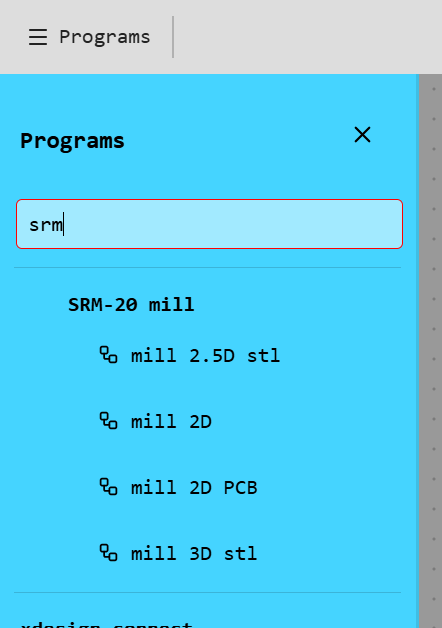
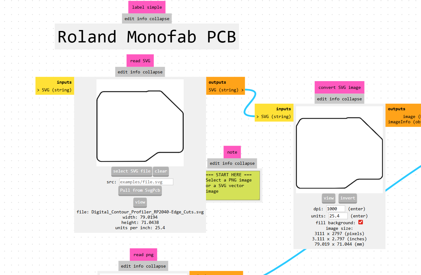
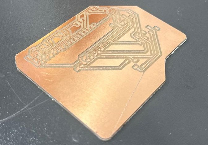
Select SRM-20 mill > PCB
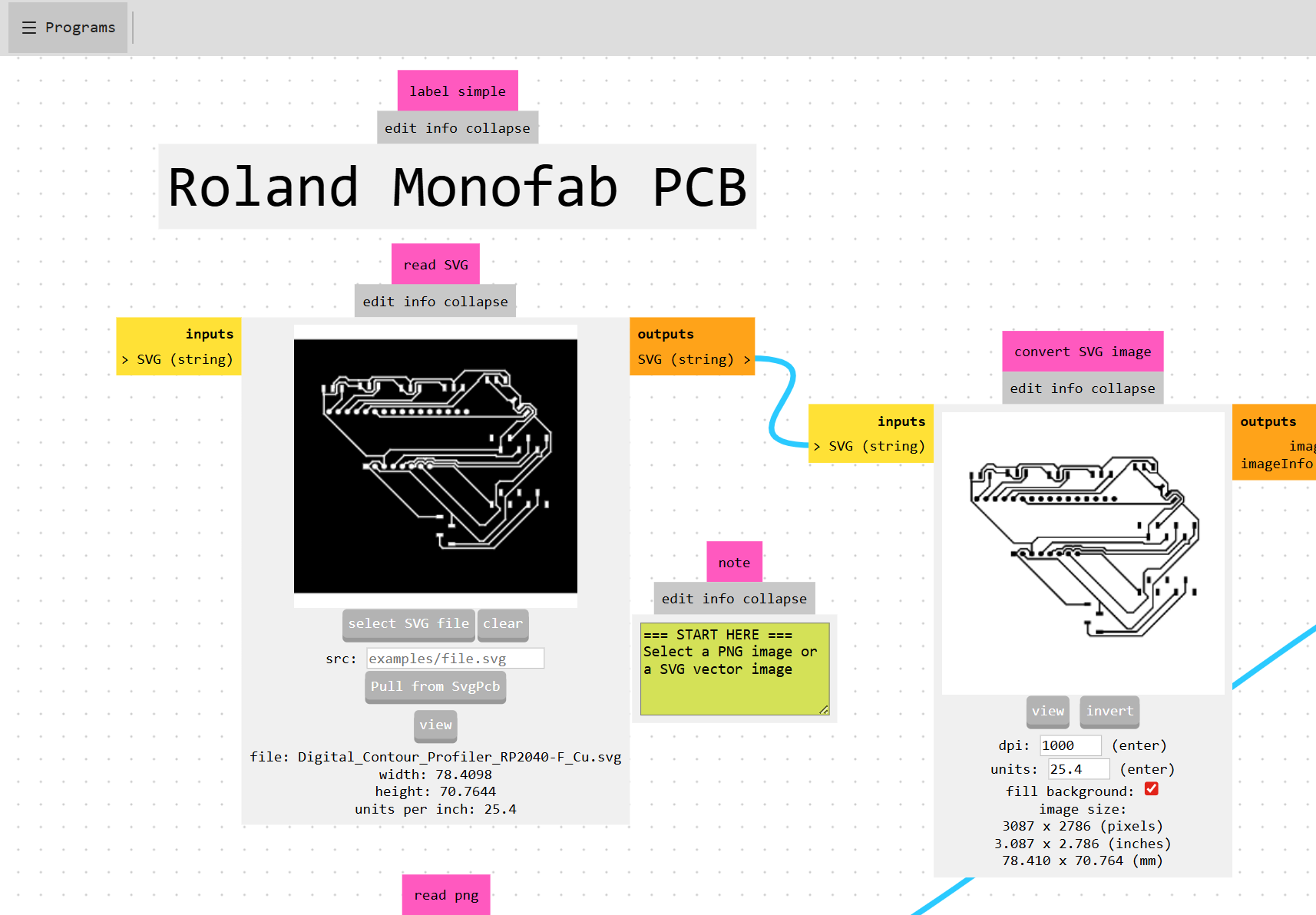
Upload SVG / Notice Invert effect (white is milled/black is kept..good for traces)
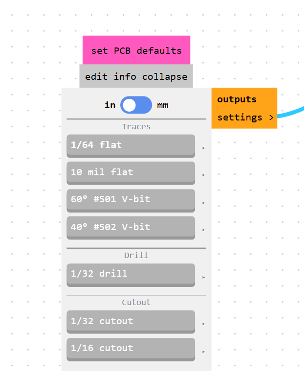
PCB Defaults (1/64 for tracess , 1/32 for edges)
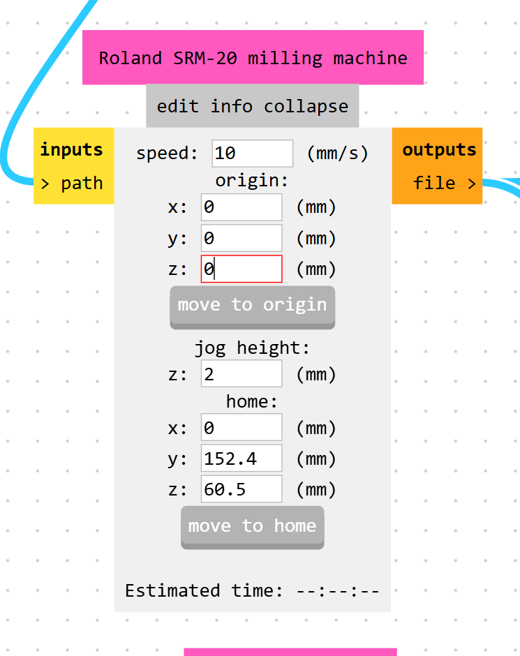
Machine parameters. make sure its 0
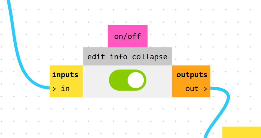
Make sure this is on to get the file saved to your pc
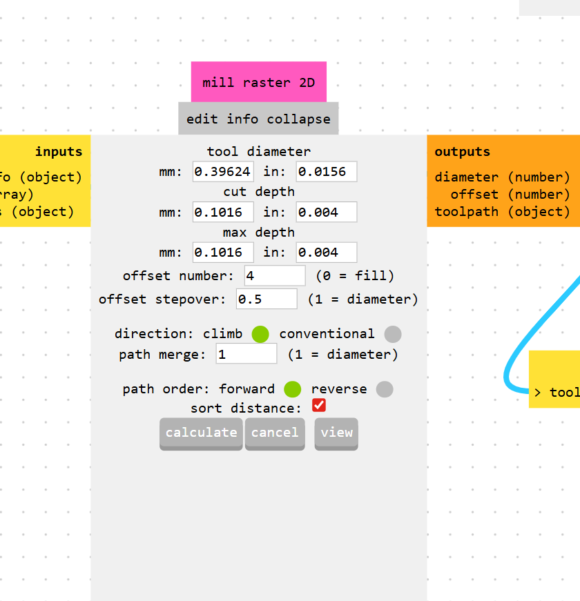
Calculate
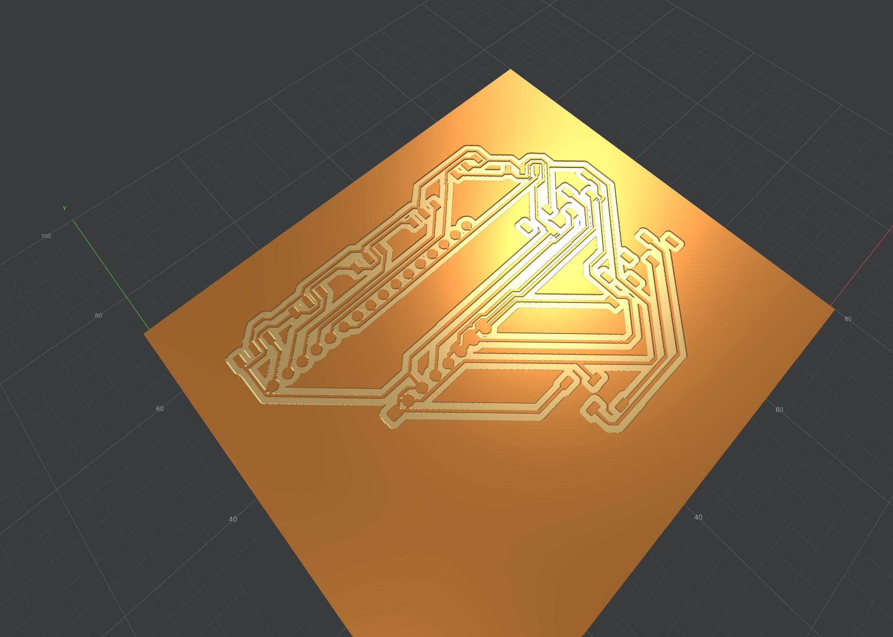
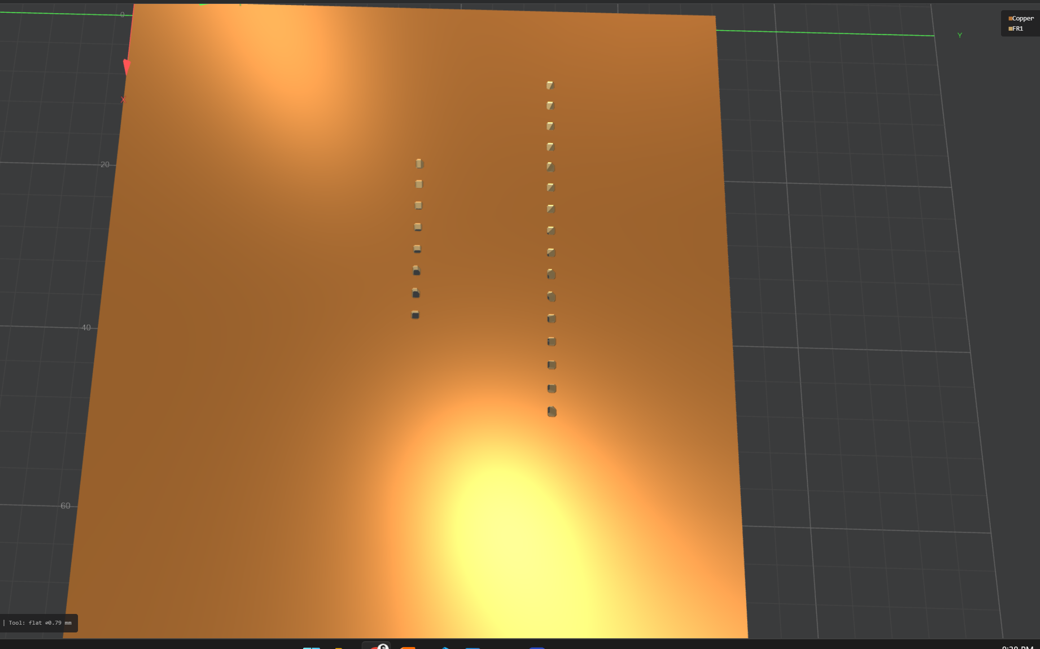
Preview
Pro Tip / Warning
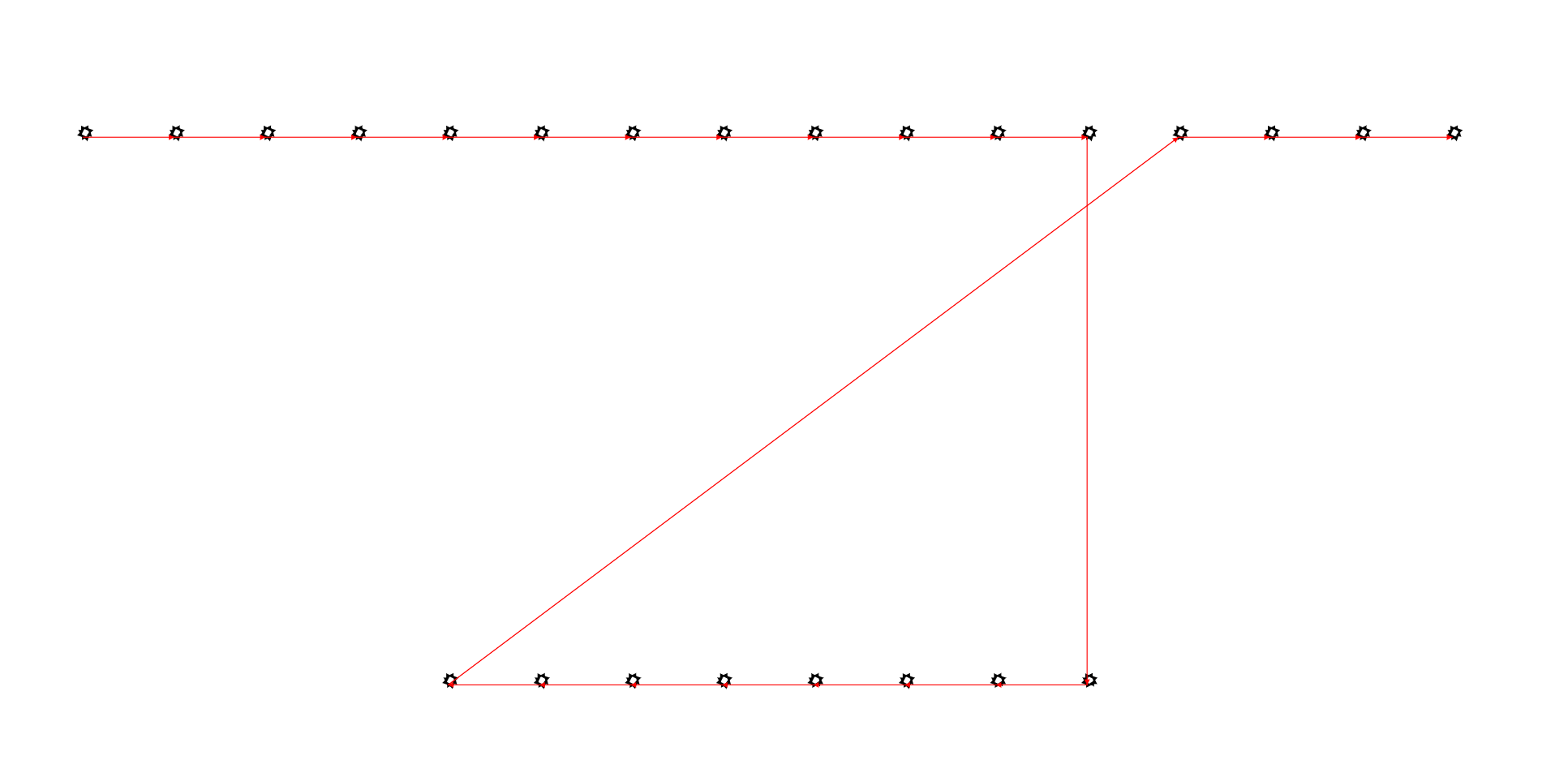
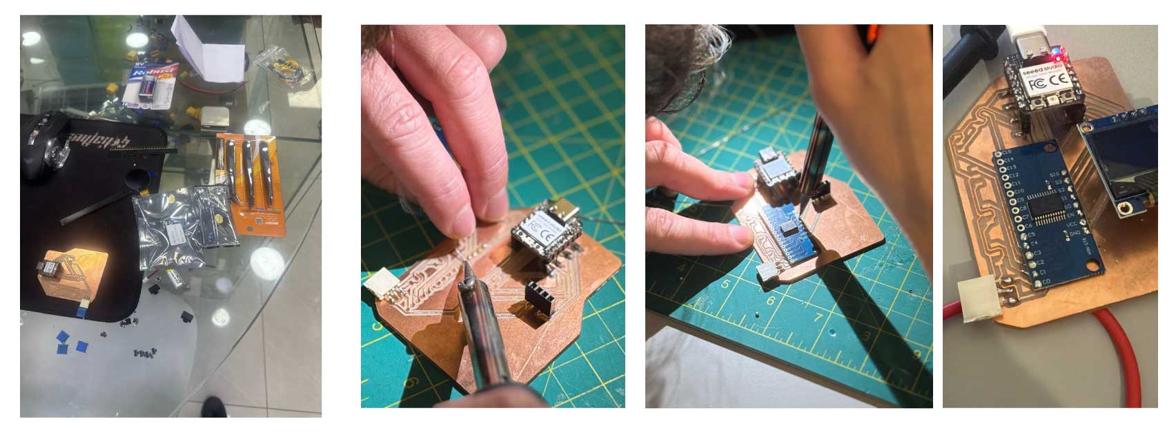
In my toolpath generated, and as per my schematic in Week 6 I am not using the full multiplexer footprint to run this PCB, I only used 4 channels of the multiplexer and the rest i did not even solder completely to the PCB.
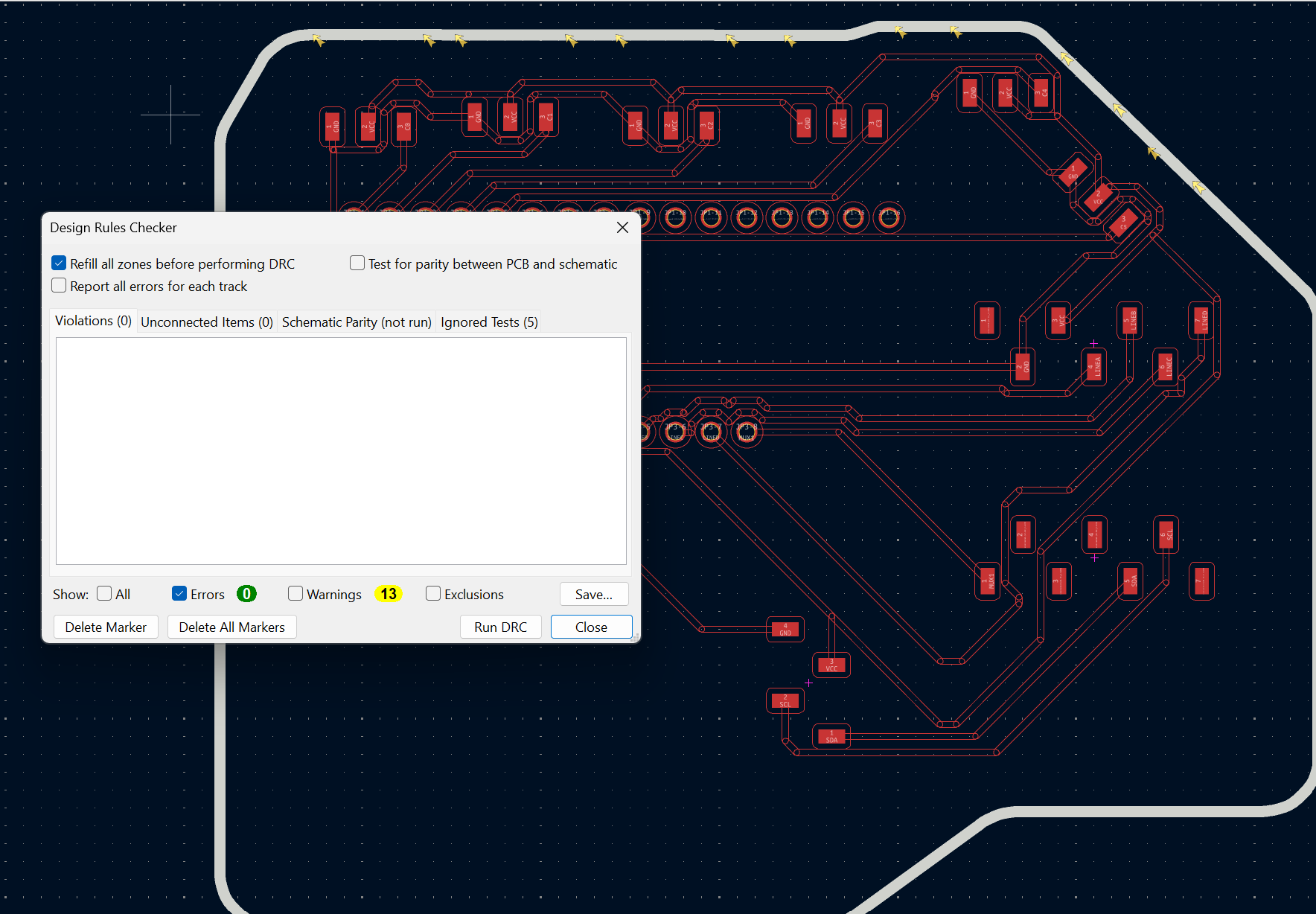
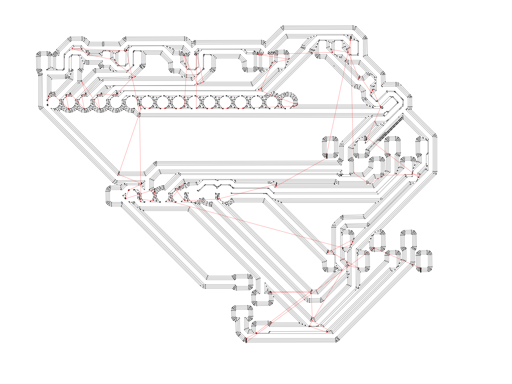
Always run DRC prior to exporting the files from KiCAD, mainly addressing any errors found
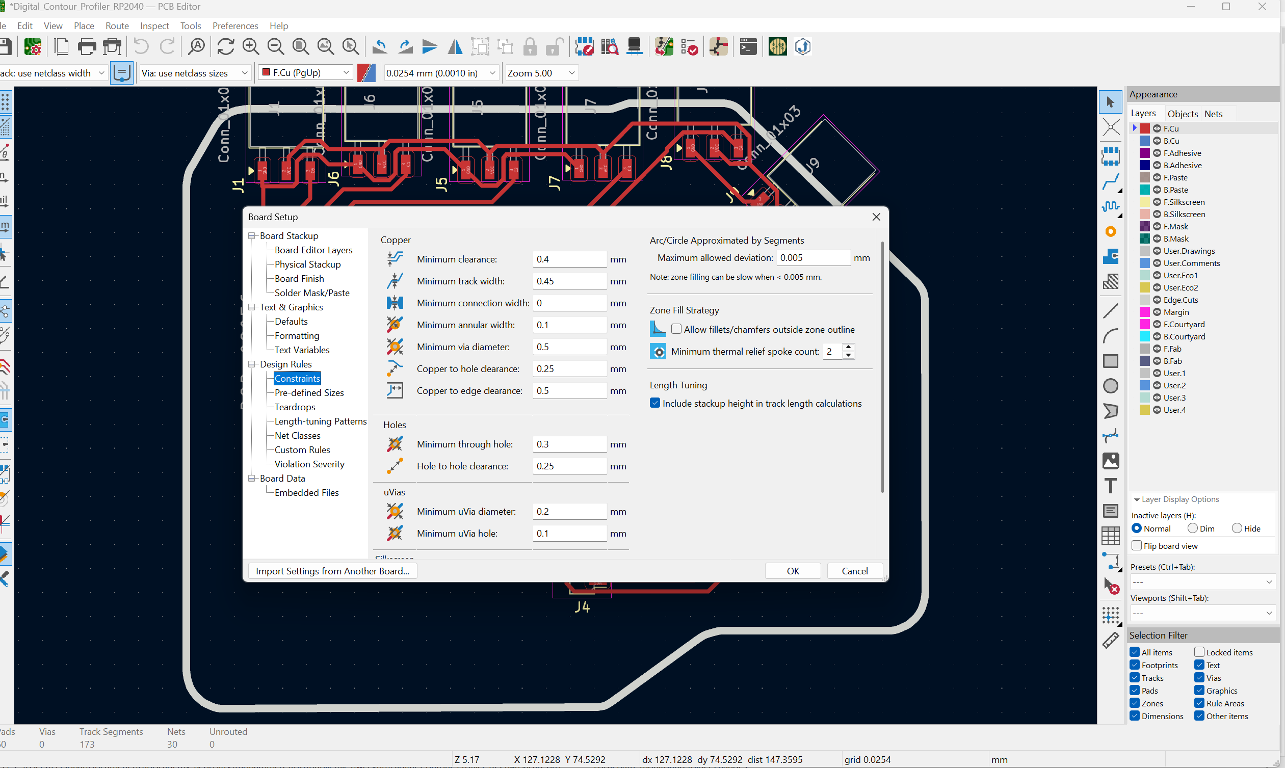
Double checking the constraints , clearance and minimum trace width
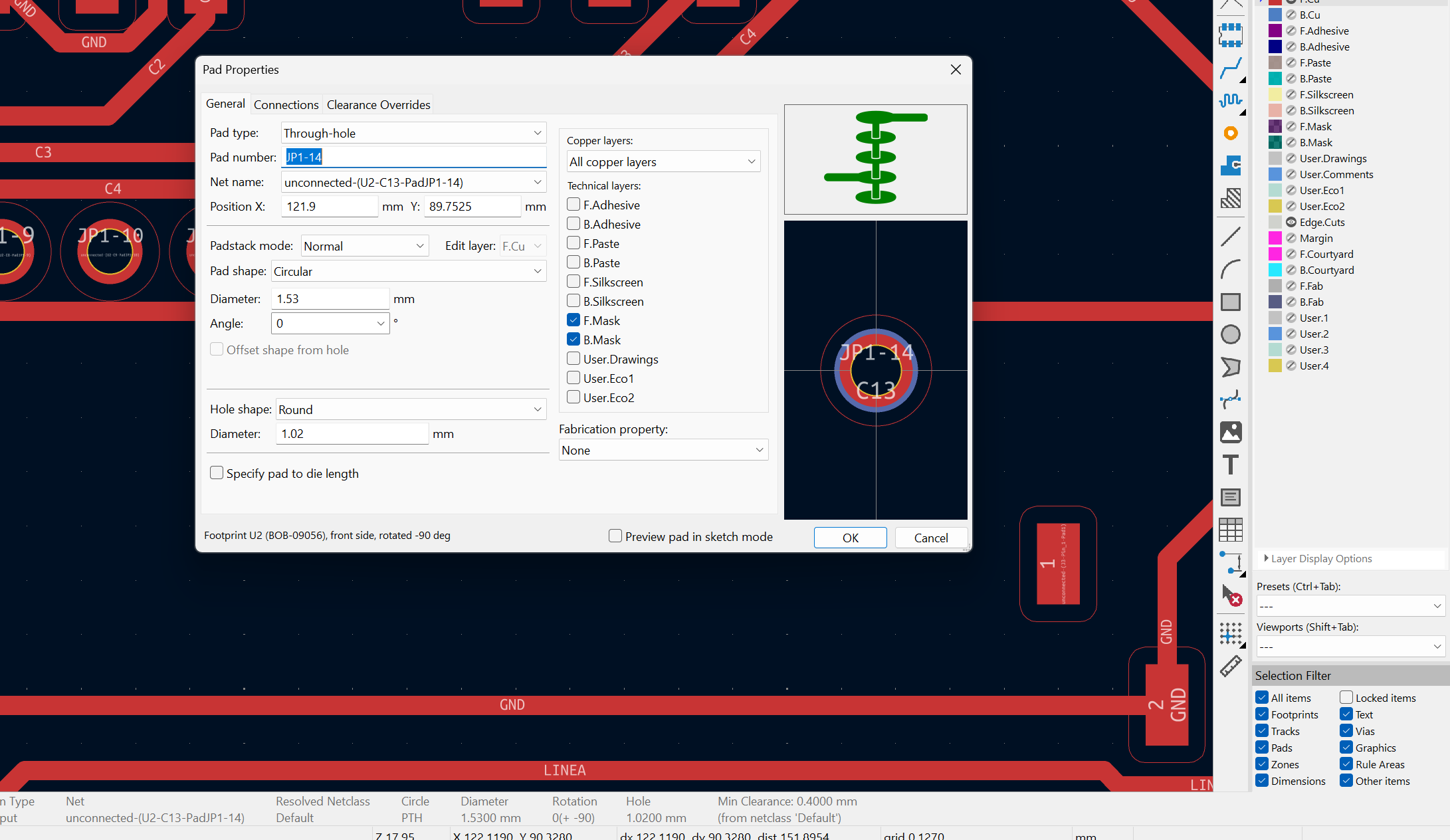
Pad properties to ensure layer / diamaeter
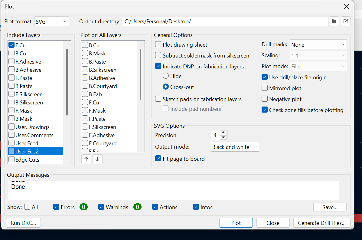
Plot Settings, Note:Use Drill/place file origin and Fit to page,change drill marks to Actual Size
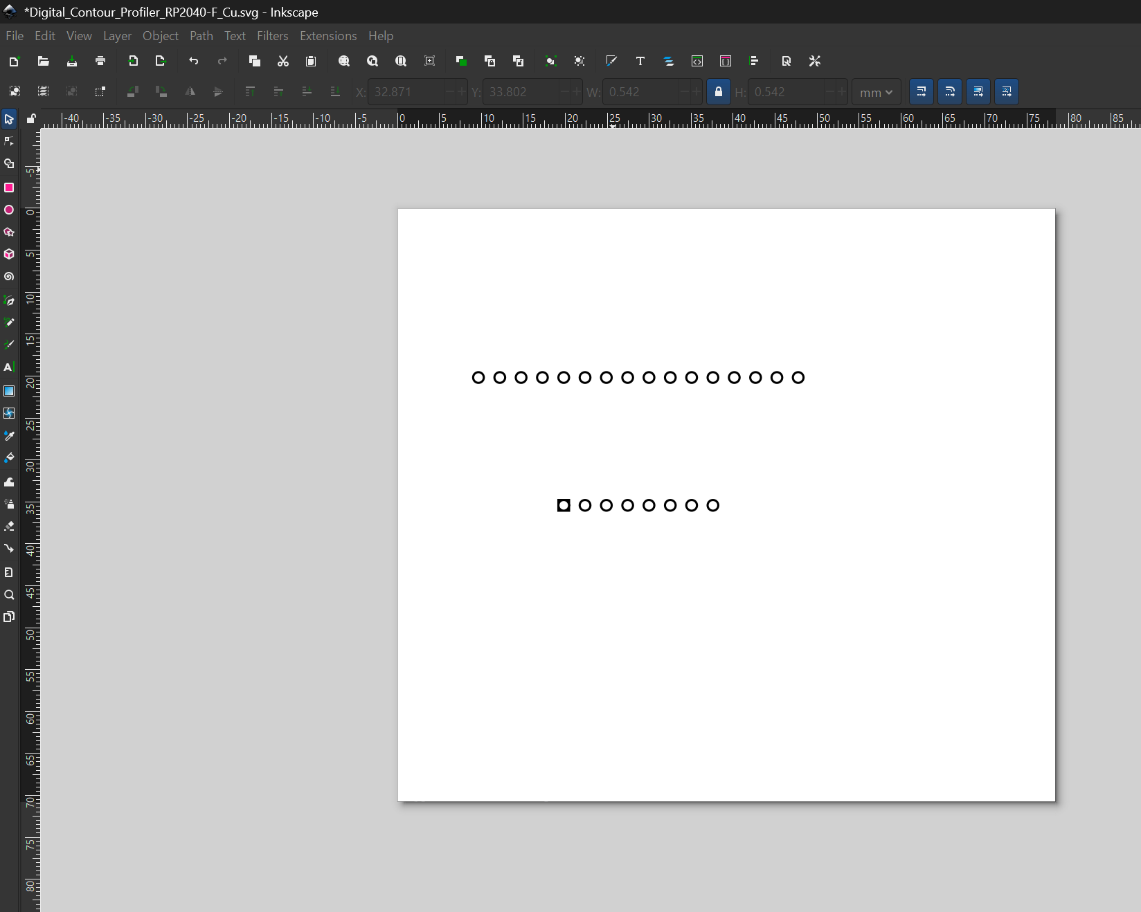
Inkscape post-processing
Preview
Edge settings , notice no black is cutting, white is left space
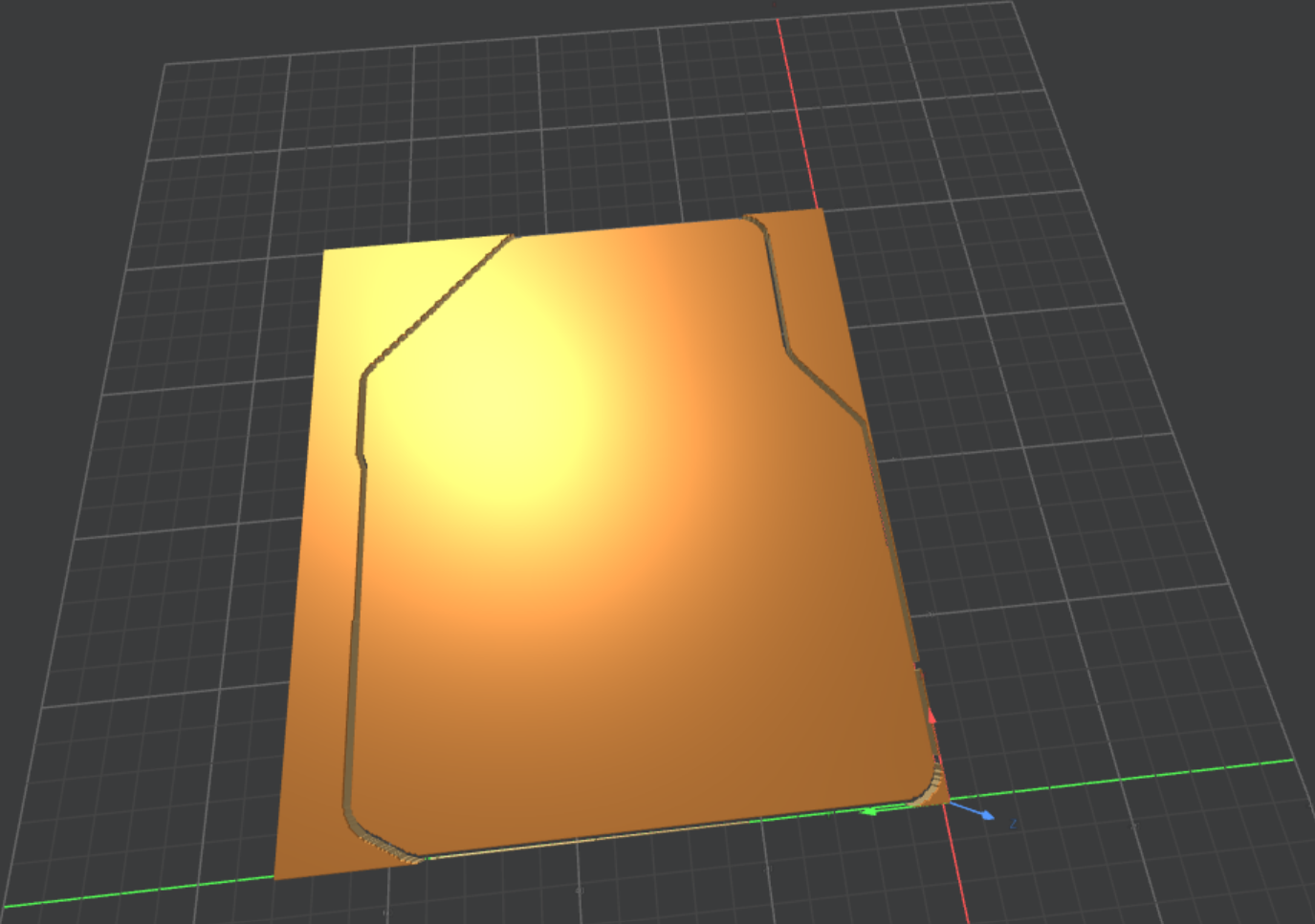
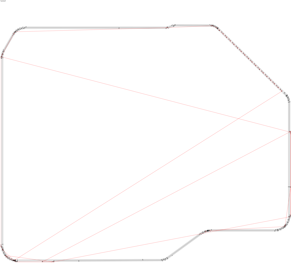
Edge Preview
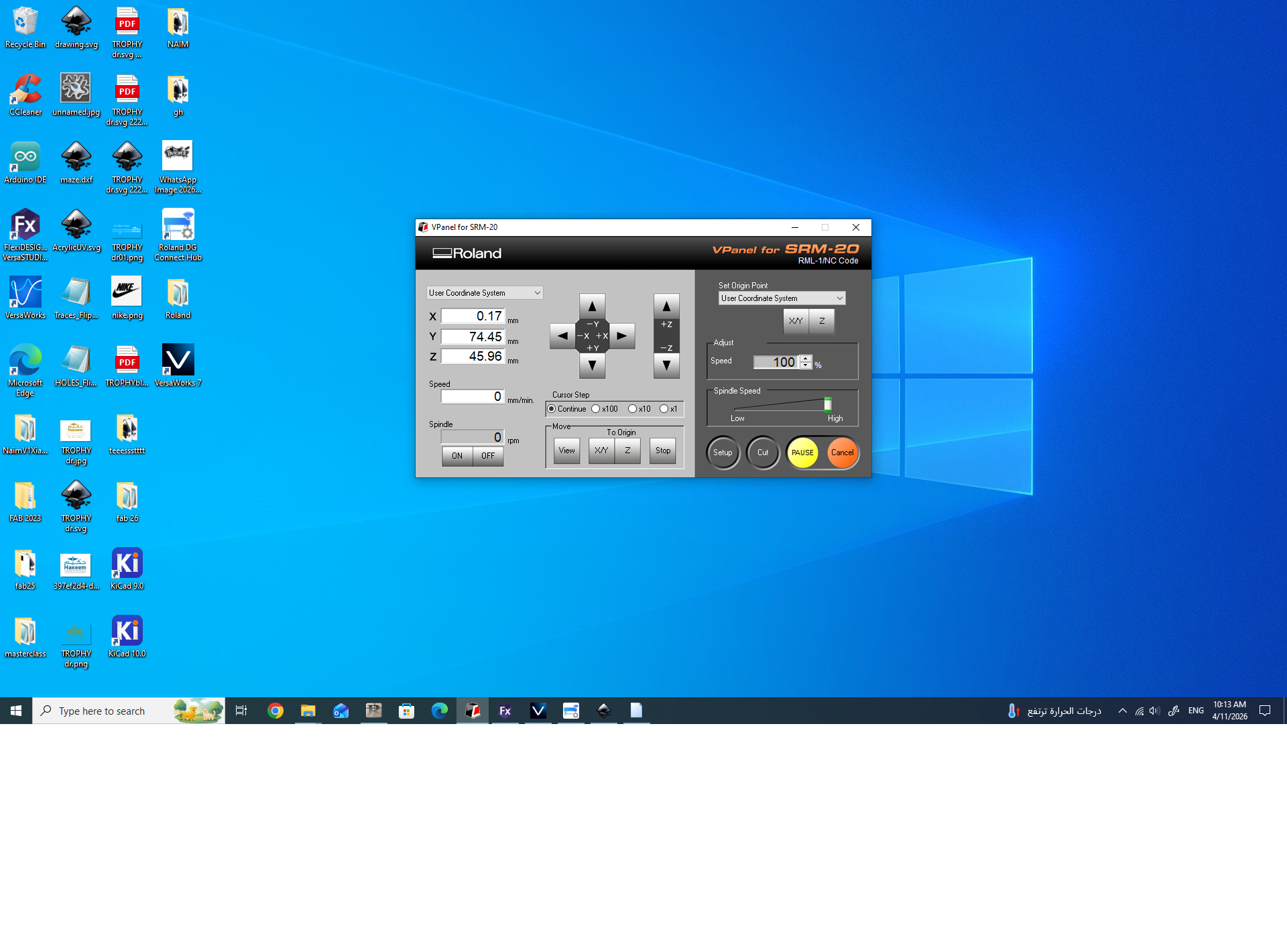
Setting and Defining Zero (xy)-Click on Set to Origin Point,repeat process for Z
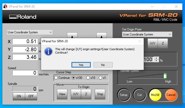
Setting and Defining Zero (xy)-Confirm , repeat process for Z
Zeros Set
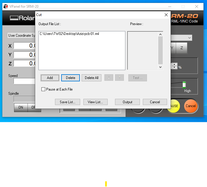
Load the program
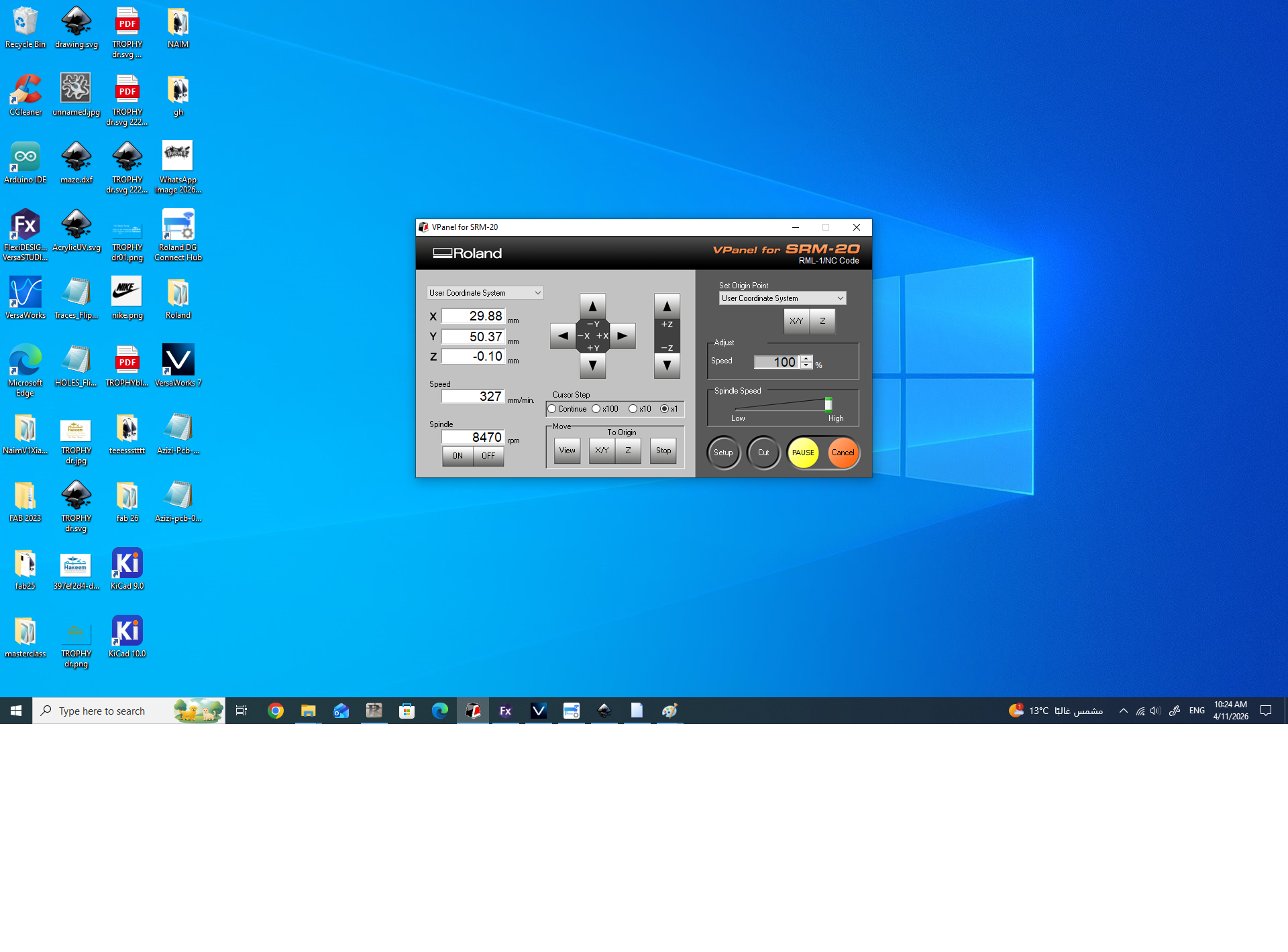
While Cutting
game-test.ino
           #include
#include
#include

#define SCREEN_WIDTH 128
#define SCREEN_HEIGHT 64
#define SCREEN_ADDRESS 0x3C

// --- MUX CONTROL PINS ---
const int S0 = 0; const int S1 = 1; const int S2 = 2; const int S3 = 3;
const int SIG_PIN = 26; // MUX1 (A0)

Adafruit_SSD1306 display(SCREEN_WIDTH, SCREEN_HEIGHT, &Wire, -1);

void setup() {
  Wire.setSDA(6); Wire.setSCL(7); Wire.begin();
  pinMode(S0, OUTPUT); pinMode(S1, OUTPUT);
  pinMode(S2, OUTPUT); pinMode(S3, OUTPUT);

  analogReadResolution(10); // Standard 10-bit range (0-1023)

  if(!display.begin(SSD1306_SWITCHCAPVCC, SCREEN_ADDRESS)) for(;;);
  display.clearDisplay();
  display.setTextColor(SSD1306_WHITE);
}

void loop() {
  // Select J1 (Channel 0)
  digitalWrite(S0, LOW); digitalWrite(S1, LOW);
  digitalWrite(S2, LOW); digitalWrite(S3, LOW);

  delay(10);
  int raw = analogRead(SIG_PIN);

  // Convert raw value to Voltage
  // Formula: (Raw Value / 1023.0) * 3.3 Volts
  float voltage = (raw / 1023.0) * 3.3;

  display.clearDisplay();

  // Header
  display.setTextSize(1);
  display.setCursor(0, 0);
  display.println("VOLTMETER MODE (J1)");
  display.println("---------------------");

  // Display Voltage
  display.setCursor(0, 25);
  display.setTextSize(2);
  display.print(voltage, 2); // Show 2 decimal places
  display.println(" V");

  // Display Raw for comparison
  display.setTextSize(1);
  display.setCursor(0, 50);
  display.print("Raw ADC: ");
  display.print(raw);

  // Visual Level Bar
  int barWidth = map(raw, 0, 1023, 0, 60);
  display.drawRect(65, 50, 60, 8, SSD1306_WHITE);
  display.fillRect(65, 50, barWidth, 8, SSD1306_WHITE);

  display.display();
  delay(100);
}