// Week 06
Electronics Design
Introduction
In Week 06, focused on electronic design, I learned how to design an electronic circuit board from scratch using Electronic Design Automation (EDA) software. This week was divided into two main parts: Group Assignment and Individual Assignment. The goal was to understand how a microcontroller functions and how to design a PCB capable of interacting with input and output devices.
Objectives
Group Assignment
- Use lab test equipment to observe a microcontroller circuit board.
- Demonstrate the use of a Logic Analyzer and test instruments.
- Document group work and reflect individually.
Individual Assignment
- Use an EDA tool (KiCad) to design a development board from scratch.
- Select and integrate inventory components.
- Include local input and output interface devices.
Tools & Technologies
1. KiCad (EDA Software)
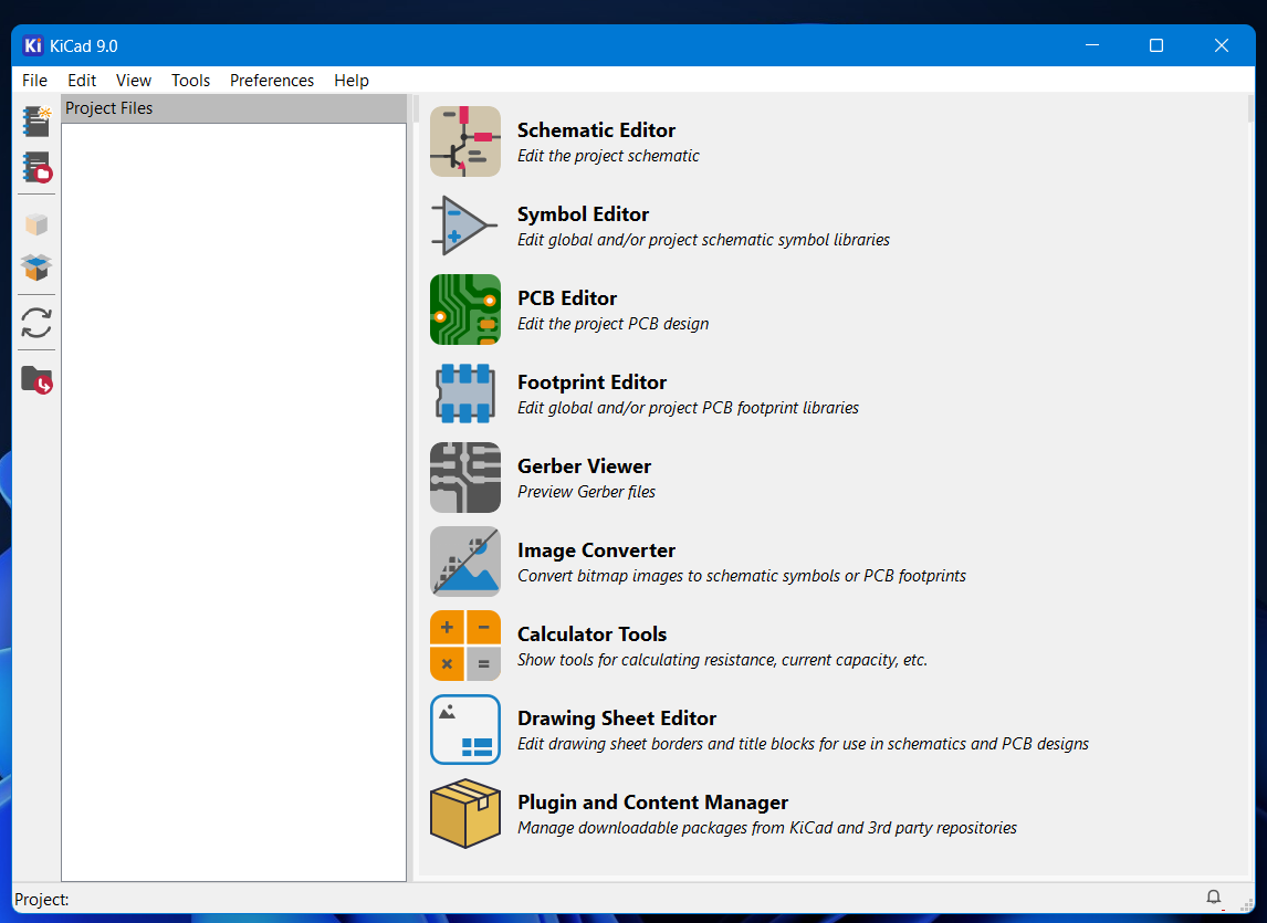
KiCad is an open-source Electronic Design Automation (EDA) software suite used for schematic capture and PCB layout design. I downloaded and installed it from the official site to set up my environment.
2. Logic Analyzer & Test Equipment
Test instruments such as digital oscilloscopes and multimeters capture and display electrical logic signals. We used the oscilloscope to observe real-time digital square waves from our microcontroller and a digital multimeter to measure voltage, current, resistance, and verify electrical continuity across traces.
3. XIAO RP2040 Microcontroller
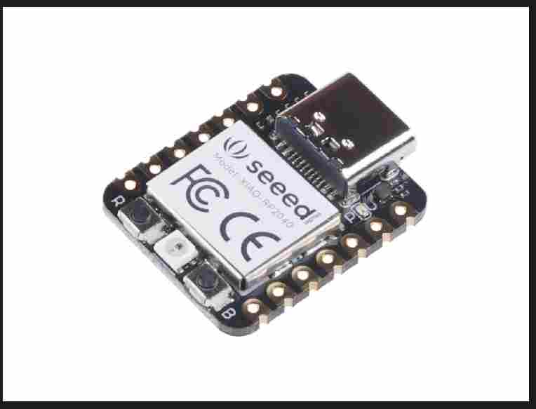
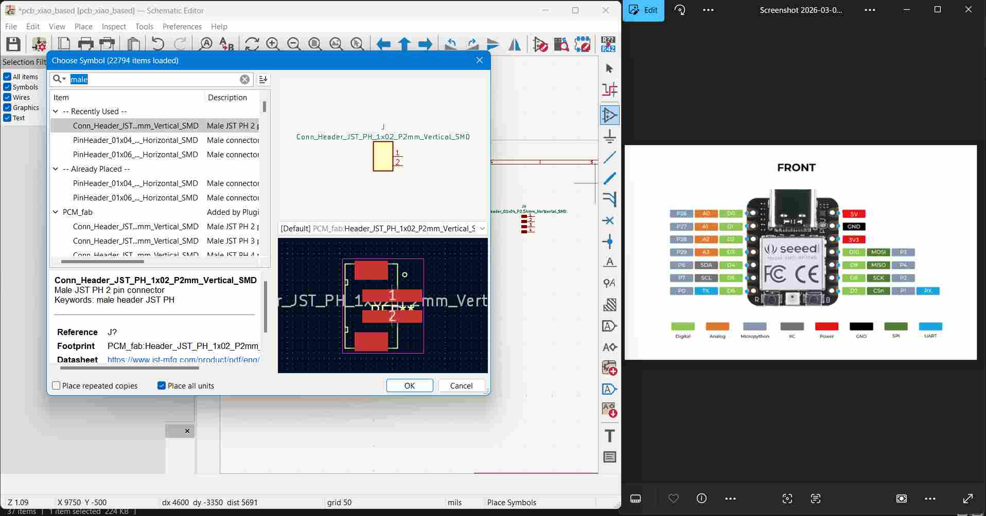
I selected the Seeed Studio XIAO RP2040 microcontroller. Built around the Raspberry Pi RP2040 chip, it features dual ARM Cortex-M0+ cores, USB-C connectivity, and supports I2C (SCL/SDA), SPI (MISO/MOSI/CS/SCK), and UART (TX/RX) buses alongside 3.3V logic and 5V USB power delivery.
Process & Workflow
Group Assignment
At Fab Lab Rwanda – Kigali, we used various electronic test instruments to observe and analyze signals on a microcontroller board, aiming to understand physical logic behavior during debugging.
Test Equipment Used
1. Oscilloscope
Visualizes voltage fluctuations over time as waveforms. We used it to:
- View digital square wave signals.
- Measure operational frequency and peak-to-peak amplitude.
- Analyze signal transition timing and rise/fall edges.
- Compare distinct analog vs. digital waveforms.
2. Function Generator
Synthesizes controlled electrical test signals, including:
- Sine waves
- Square waves
- Triangle waves
- Sawtooth waves
- Amplitude Modulated (AM) signals
3. Multimeter
Used to measure DC voltage levels, check trace resistance, and confirm net continuity.
4. Power Supply
Provides stable DC voltage to prevent logic signal distortion or unwanted reset cycles.
Observing Digital Signal from ESP32
We programmed an ESP32 microcontroller to output a digital switching signal. Connected to the oscilloscope, it displayed a crisp square wave toggling cleanly between HIGH (3.3V) and LOW (0V).
Amplitude Modulation (AM) Signal
Using the function generator, we generated an AM signal to observe high-frequency carrier modulation over an envelope signal, demonstrating signal conditioning principles.
Analog and Sawtooth Signals
By contrasting waveform profiles, we noted key operational distinctions:
- Sine waves provide smooth, continuous transitions.
- Square waves switch instantly between high and low logic thresholds.
- Sawtooth waves ramp up linearly before abruptly dropping to ground.
Group Reflection
Visualizing real-time digital logic from the ESP32 bridged theoretical circuit design with physical hardware measurement. Review the full analysis on our Week 06 Group Assignment Page.
Individual Assignment
For the individual task, I designed a custom development board incorporating the XIAO RP2040 MCU, current-limited output LEDs, a slide switch input, and expansion headers.
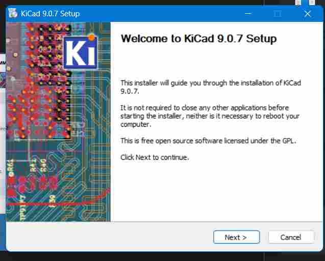
Step 1: Download and Install KiCad
Installed KiCad EDA with administrative privileges to configure library paths and local device definitions.

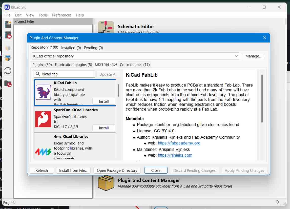
Step 2: Install Fab Electronics Library
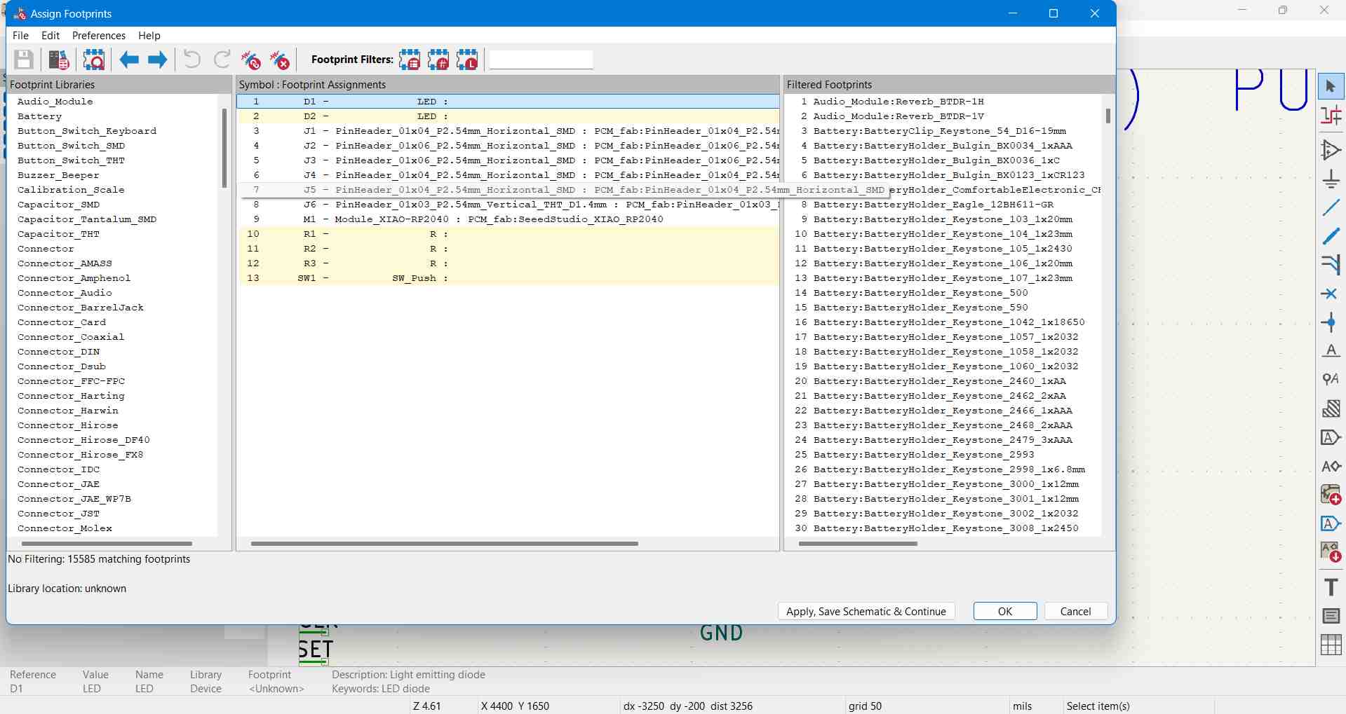
Extracted and linked the official Fab Academy footprint and symbol library into KiCad's Symbol and Footprint Managers to access surface-mount component models.
Step 3: Microcontroller Pin Mapping & Datasheet Analysis
Reviewed the official Seeed Studio XIAO RP2040 Documentation to confirm pin constraints, power routing, and peripheral muxing rules.
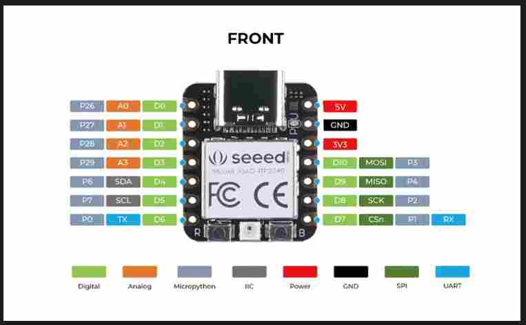
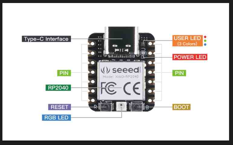
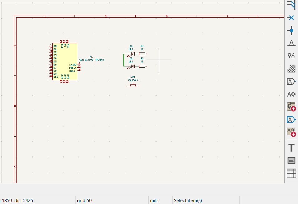
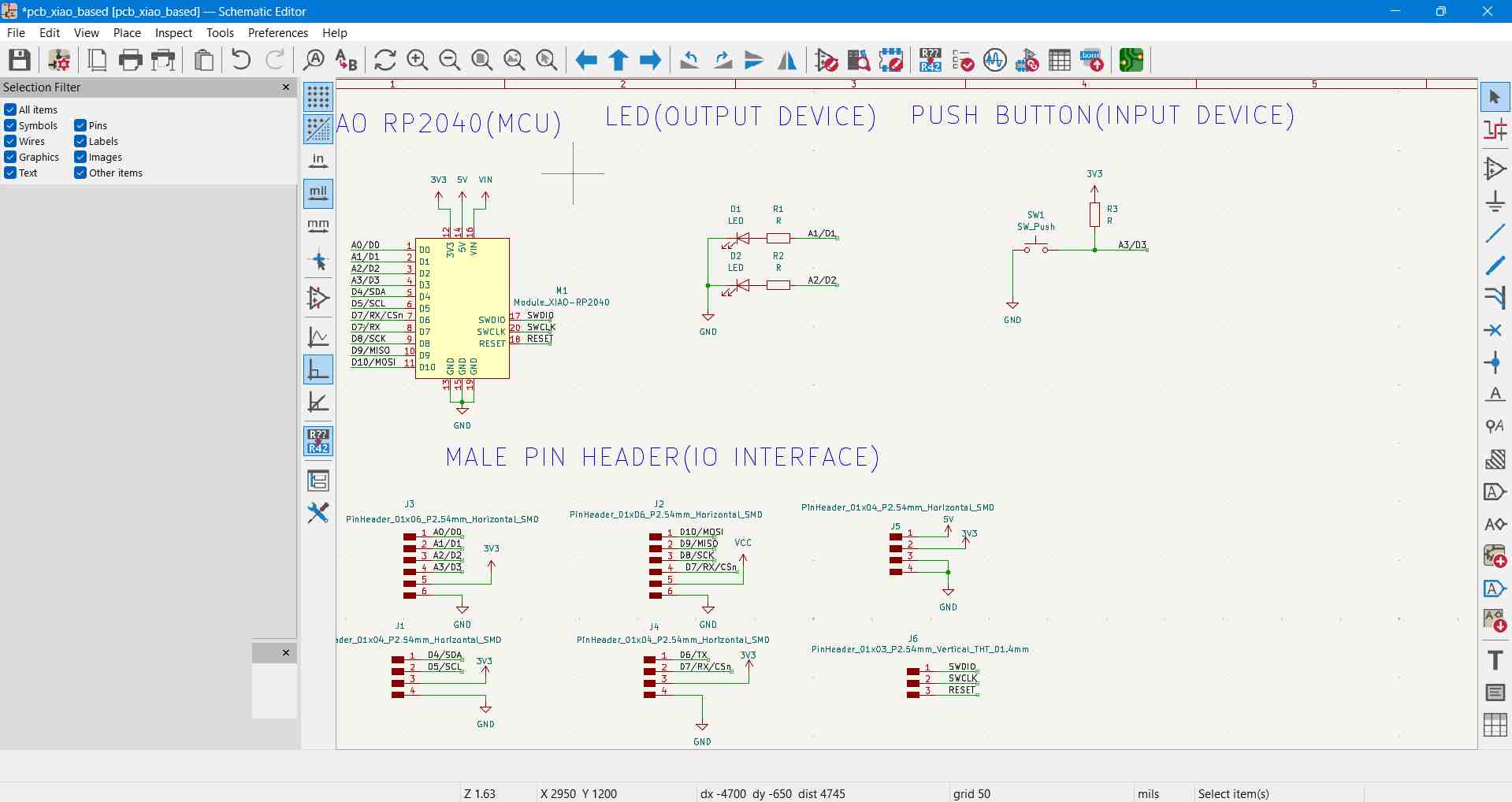
Step 4: Schematic Design
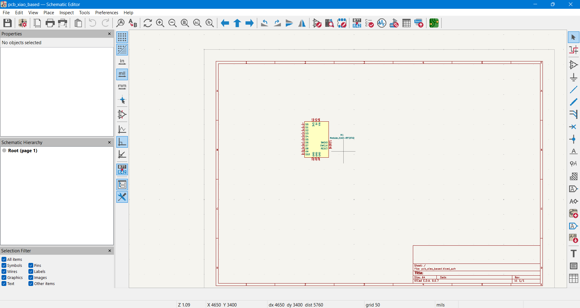
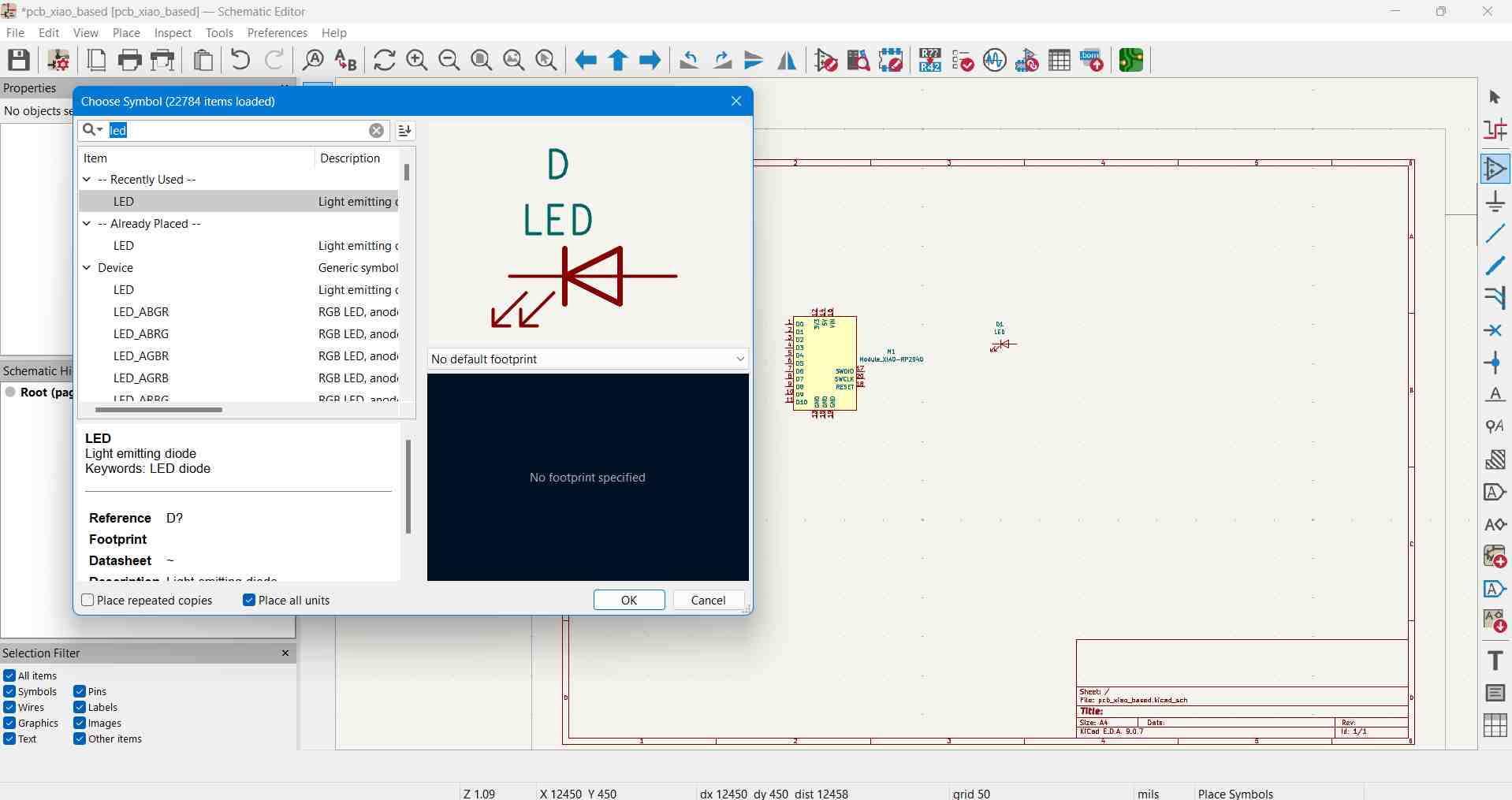
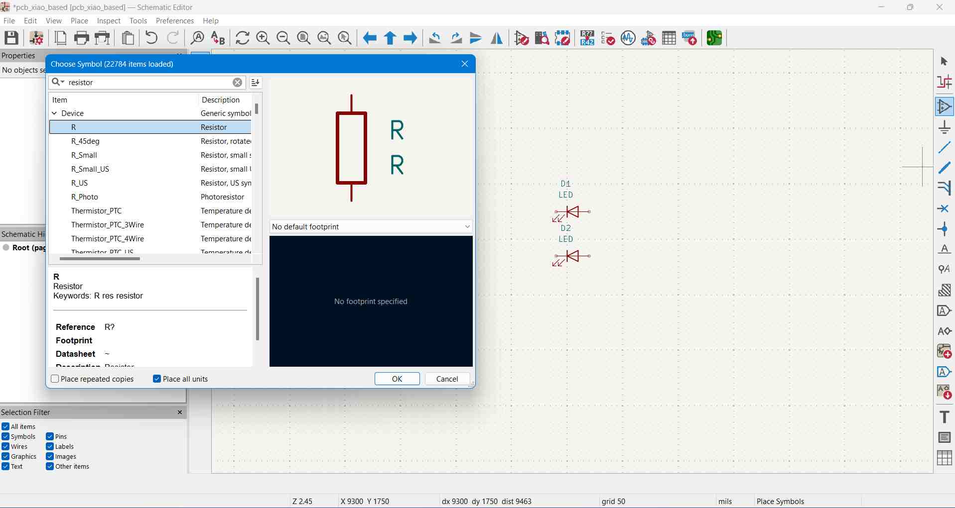
Constructed the logical circuit diagram by selecting components from the library:
- XIAO RP2040: Main system controller.
- Two Surface-Mount LEDs: Status output indicators.
- Slide Switch: Digital user input interface.
- Current-Limiting Resistors: Protection for LEDs and pull-down references.
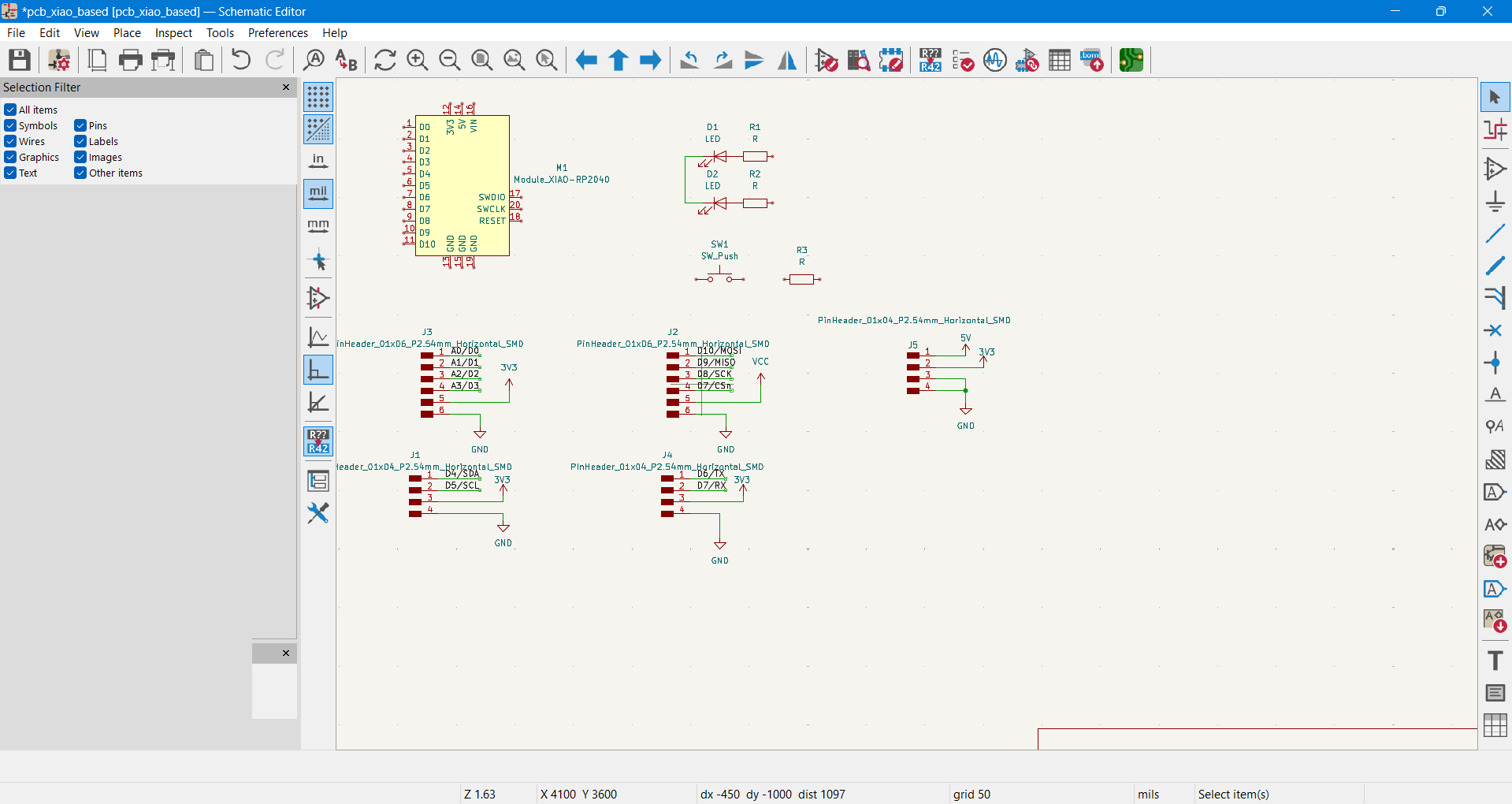
- Pin Headers: Standard 0.1" pitch breakout headers for future expansion.
Referenced pinout specs during connection routing:
Completed the full schematic and matched all electronic components with surface-mount footprints:
Step 5: Update PCB from Schematic
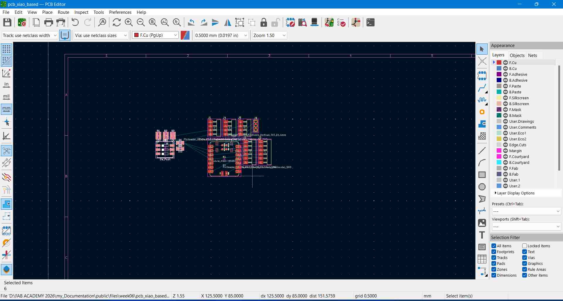
Transferred netlist connections into the PCB Layout Editor using Update PCB from Schematic. Components appeared linked by ratsnest connection wires.
Step 6: Component Placement
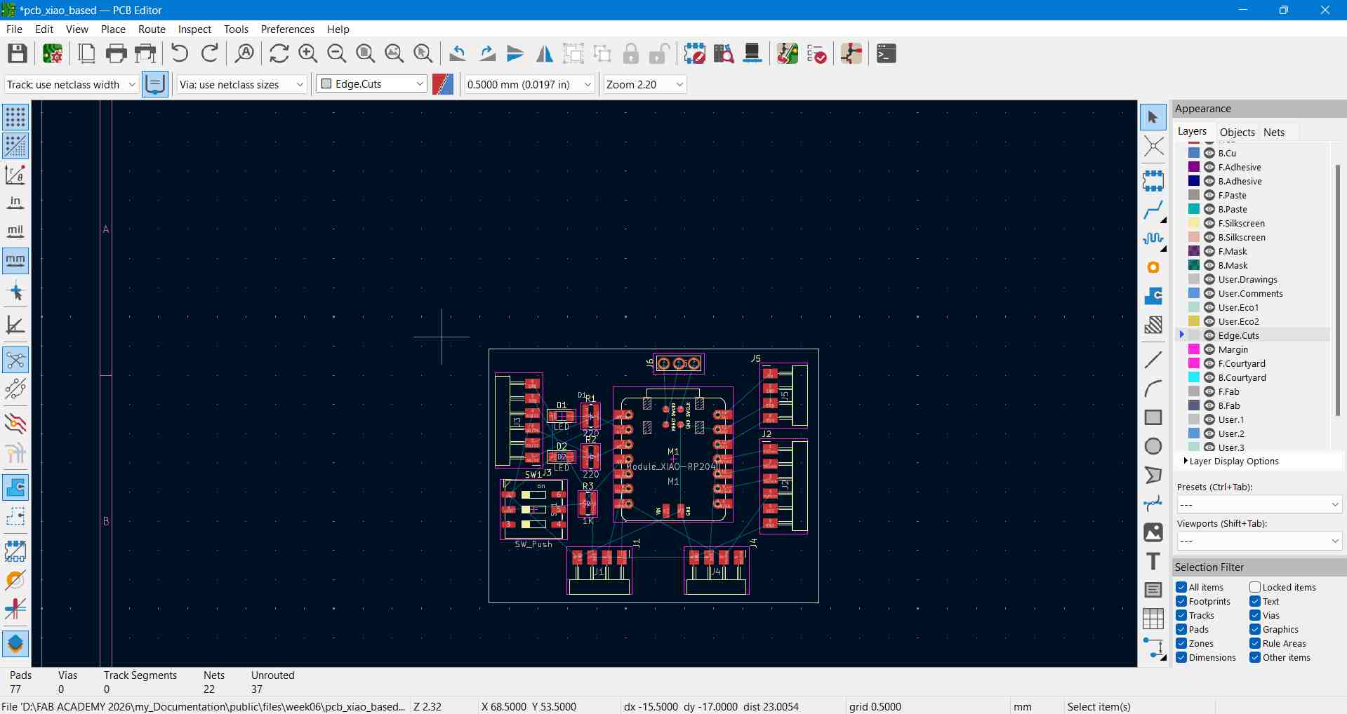
Placed the XIAO RP2040 centrally, aligning LEDs and headers along exterior board margins for easy routing access.
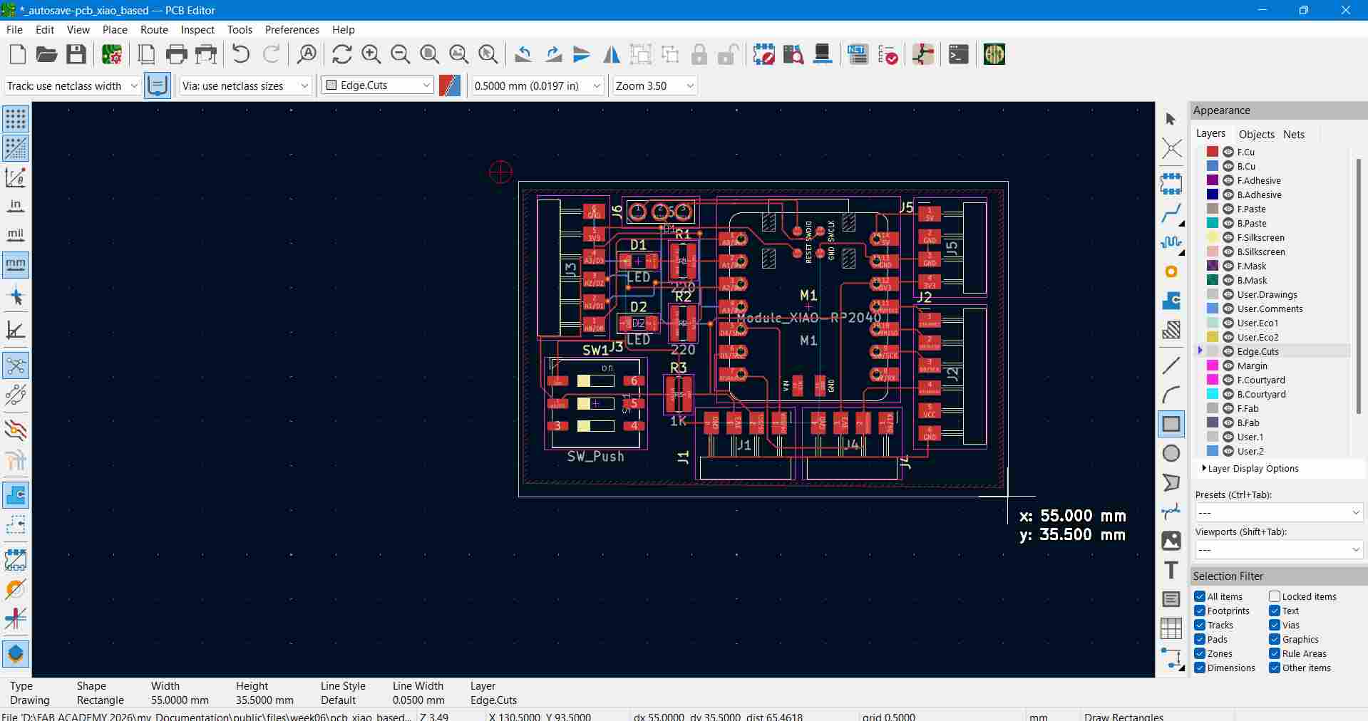
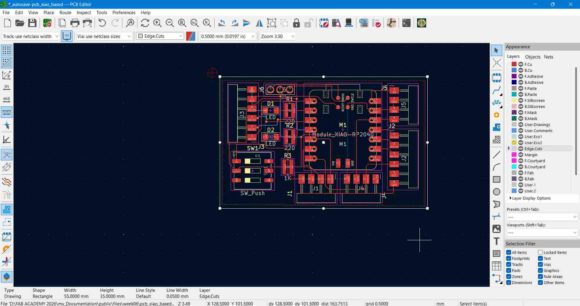
Step 7: Defining Board Outline (Edge.Cuts)
Drew a clean rectangular boundary on the Edge.Cuts layer, leaving ample clearance around peripheral pads for milling isolation.
Step 8: Routing PCB Traces
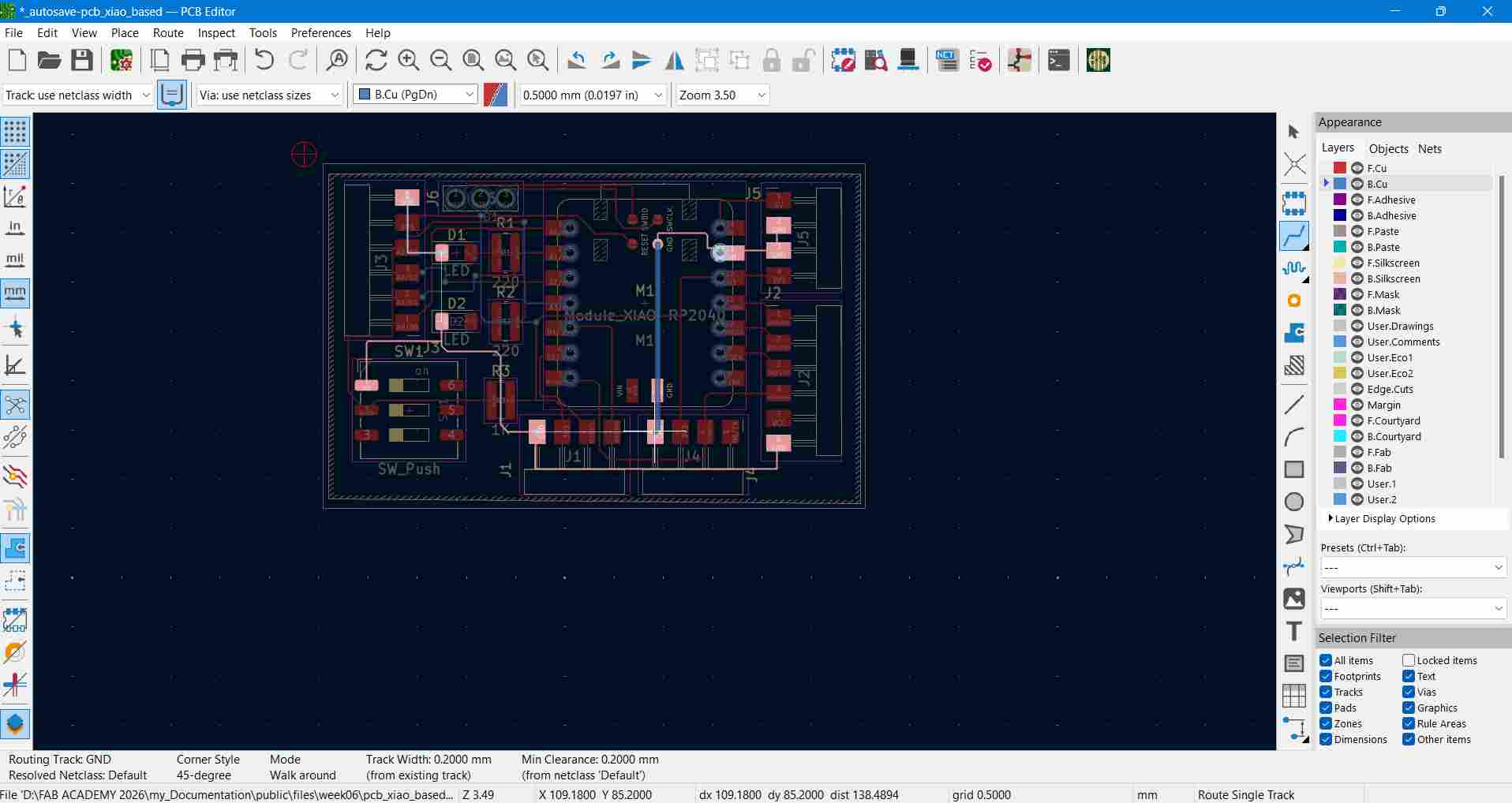
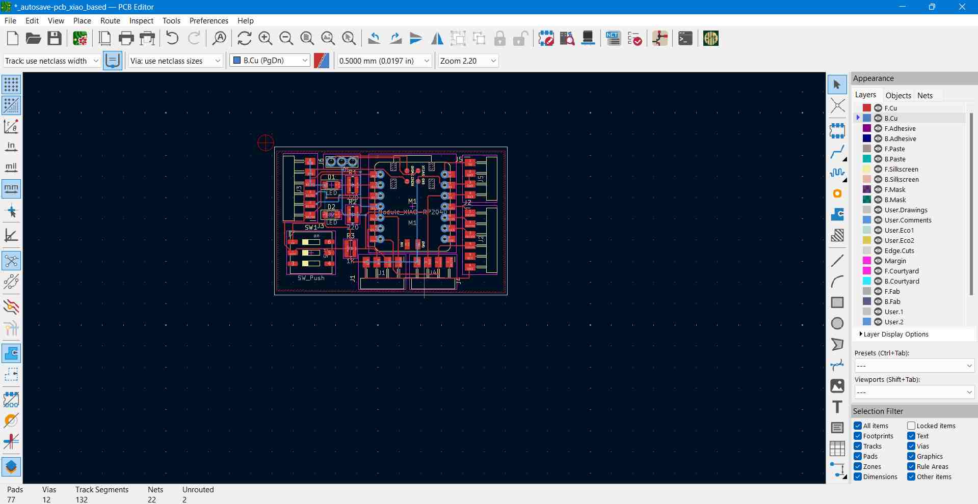
Routed copper traces manually using a track width of 0.6 mm to guarantee clean isolation passes on the lab CNC PCB mill.
Step 9: Design Rule Check (DRC)
Configured clearance constraints to 0.4 mm (matching our 1/64" milling endmill bit) and executed the DRC tool to resolve trace clearance errors and unconnected nets.
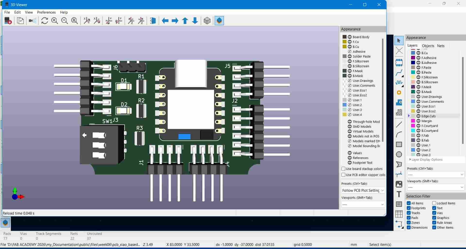
Step 10: 3D Inspection & Verification
Inspected the board assembly within the KiCad 3D Viewer to verify physical component heights, mechanical clearances, and USB connector accessibility.
Challenges & Problem Solving
- Navigating and mastering the KiCad EDA workflow interface for the first time.
- Importing and mapping third-party symbol and footprint libraries correctly.
- Routing single-layer PCB tracks without creating trace intersections or needing zero-ohm jumpers.
- Interpreting microchip pin multiplexing matrix specifications directly from datasheets.
What I Learned
- Designing a complete custom PCB schematic and routing layout from scratch.
- Using KiCad EDA tools for footprint assignment, trace routing, and DRC validation.
- Measuring and troubleshooting real-time digital logic signals using an oscilloscope.
- Designing PCB layouts with manufacturing tool constraints (clearances, trace widths) in mind.
Downloads & References